The Electron Microscope: A Comprehensive Guide for Science Students

electron microscope

The electron microscope is a powerful scientific instrument that revolutionized the field of materials science and biology by enabling the visualization and analysis of structures at the atomic and molecular level. This comprehensive guide will delve into the intricate details of electron microscopy, providing science students with a deep understanding of its principles, applications, and the latest advancements in this cutting-edge technology.

Understanding the Fundamentals of Electron Microscopy

Electron microscopes operate on the principle of using a beam of accelerated electrons, rather than light, to illuminate and interact with a sample. This approach allows for much higher resolution imaging compared to traditional optical microscopes, which are limited by the wavelength of visible light.

The key components of an electron microscope include:

  1. Electron Gun: The electron gun is responsible for generating and accelerating the electron beam. It typically uses a tungsten filament or a field emission source to produce the electrons, which are then accelerated by a high voltage (typically ranging from 60 kV to 300 kV).

  2. Electromagnetic Lenses: Electromagnetic lenses, similar to the glass lenses in optical microscopes, are used to focus and manipulate the electron beam. These lenses are composed of coils of wire that create a magnetic field, which can bend the path of the electrons.

  3. Vacuum System: Electron microscopes require a high-vacuum environment to prevent the electron beam from being scattered by air molecules. This vacuum system ensures that the electrons can travel unimpeded from the electron gun to the sample and the detector.

  4. Sample Stage: The sample stage is where the specimen is placed for observation. It can be moved in three dimensions (x, y, and z) to allow for the examination of different areas of the sample.

  5. Detector: The detector, such as a scintillator-photomultiplier tube or a charge-coupled device (CCD) camera, is responsible for converting the interactions between the electron beam and the sample into a signal that can be processed and displayed as an image.

Types of Electron Microscopes

electron microscope

There are several types of electron microscopes, each with its own unique capabilities and applications:

  1. Transmission Electron Microscope (TEM): In a TEM, the electron beam passes through a thin specimen, and the transmitted or scattered electrons are detected to form an image. TEMs can achieve extremely high resolutions, down to the atomic scale, making them invaluable for studying the structure of materials and biological samples.

  2. Scanning Electron Microscope (SEM): In an SEM, the electron beam scans the surface of a sample, and the secondary or backscattered electrons are detected to create a three-dimensional image of the sample’s topography. SEMs are widely used for surface analysis and characterization of materials.

  3. Scanning Transmission Electron Microscope (STEM): STEM combines the principles of both TEM and SEM, where the electron beam is focused into a small spot and scanned across the sample. This allows for high-resolution imaging and the ability to perform analytical techniques, such as energy-dispersive X-ray spectroscopy (EDS), to determine the elemental composition of the sample.

  4. Cryo-Electron Microscope (Cryo-EM): Cryo-EM is a specialized technique where the sample is cooled to cryogenic temperatures, typically using liquid nitrogen or liquid helium. This approach helps to preserve the native structure of biological samples, such as proteins and macromolecular complexes, allowing for high-resolution imaging and structural analysis.

Resolution and Image Quality in Electron Microscopy

The resolution of an electron microscope is a critical factor in its performance, as it determines the level of detail that can be observed in the resulting image. The resolution of an electron microscope is typically measured in angstroms (Å) or nanometers (nm), with the best modern instruments capable of achieving sub-ångström resolution.

The factors that influence the resolution of an electron microscope include:

  1. Electron Beam Energy: Higher electron beam energies (e.g., 200 kV or 300 kV) generally result in higher resolutions due to the shorter wavelength of the electrons.

  2. Lens Aberrations: Imperfections in the electromagnetic lenses, such as spherical and chromatic aberrations, can limit the achievable resolution. Advances in lens design and aberration correction techniques have significantly improved the resolution of modern electron microscopes.

  3. Specimen Preparation: The way the sample is prepared and mounted can also affect the resolution. Proper sample preparation techniques, such as thin sectioning, staining, and cryogenic freezing, are crucial for obtaining high-quality images.

  4. Environmental Factors: Factors such as vibrations, electromagnetic interference, and thermal instability can degrade the resolution of an electron microscope. Careful control of the microscope’s environment is essential for achieving the best possible image quality.

To evaluate the quality and consistency of the results obtained from electron microscopy, various resolution measures are used, including:

  1. Fourier Ring Correlation (FRC): FRC is a widely used method that evaluates the correlation between two independent reconstructions of a macromolecular structure in the Fourier domain. It provides a quantitative assessment of the resolution and the signal-to-noise ratio (SNR) of the reconstruction.

  2. Q-factor: The Q-factor is a measure of the consistency between the experimental data and the computed density map. It is calculated as the ratio of the Fourier transform of the experimental data to the Fourier transform of the computed map, and it provides a measure of the overall quality of the reconstruction.

  3. Differential Phase Residual (DPR): DPR is a resolution measure that evaluates the consistency of the phase information in the Fourier domain. It is particularly useful for assessing the resolution of cryo-EM reconstructions, where the phase information is crucial for determining the structure of macromolecular complexes.

These resolution measures are essential for understanding the quality and limitations of the data obtained from electron microscopy experiments, and they guide the optimization of the data processing and reconstruction algorithms.

Advances in Electron Microscopy Techniques

The field of electron microscopy is constantly evolving, with researchers and engineers continuously pushing the boundaries of what is possible. Some of the recent advancements in electron microscopy include:

  1. Electron Counting Detectors: The development of electron counting detectors, such as direct electron detectors, has revolutionized the field of electron microscopy. These detectors can record individual electron events, leading to improved signal-to-noise ratios and enhanced image quality, particularly in low-dose imaging applications like cryo-EM.

  2. Automated Data Processing: The increasing complexity of electron microscopy data has led to the development of automated data processing algorithms and software. These tools can streamline the analysis of large datasets, improve the consistency and reproducibility of results, and enable the extraction of more detailed information from the acquired images.

  3. Machine Learning and Artificial Intelligence: The integration of machine learning and artificial intelligence (AI) techniques into electron microscopy has opened up new possibilities for image analysis, feature extraction, and even the enhancement of image resolution. These approaches can help to overcome the limitations of traditional image processing methods and unlock new insights from electron microscopy data.

  4. In-situ and Operando Electron Microscopy: The ability to observe materials and processes in their native environments, or under operating conditions, has been a significant focus of recent advancements in electron microscopy. Techniques like in-situ heating, cooling, and gas/liquid flow cells allow researchers to study dynamic processes and the behavior of materials in real-time.

  5. Correlative Microscopy: The combination of electron microscopy with other imaging techniques, such as light microscopy, X-ray microscopy, or atomic force microscopy, has led to the development of correlative microscopy approaches. These methods enable the integration of complementary information from multiple imaging modalities, providing a more comprehensive understanding of the sample under investigation.

  6. Miniaturization and Democratization: Efforts are underway to develop more compact and affordable electron microscopes, making this powerful technology more accessible to a wider range of researchers, educators, and even citizen scientists. These advancements have the potential to democratize electron microscopy and expand its applications in various fields.

Conclusion

The electron microscope is a remarkable scientific instrument that has revolutionized our understanding of the microscopic world. This comprehensive guide has explored the fundamental principles, various types, and the critical factors that influence the resolution and image quality in electron microscopy. Additionally, it has highlighted the exciting advancements that are pushing the boundaries of this technology, from electron counting detectors to the integration of machine learning and artificial intelligence.

By understanding the intricacies of electron microscopy, science students can unlock a wealth of opportunities for cutting-edge research, materials characterization, and the exploration of the nanoscale universe. This guide serves as a valuable resource for those seeking to deepen their knowledge and expertise in this transformative field of scientific inquiry.

References:

  1. Pawel A. Penczek, “Resolution measures in molecular electron microscopy,” PMC3165049, 2010.
  2. Various authors, “Bringing into play automated electron microscopy data processing,” ScienceDirect, 2022.
  3. Various authors, “Electron counting detectors in scanning transmission electron microscopy,” Nature, 2023.
  4. Various authors, “Machine-learning approach for quantified resolvability enhancement in scanning transmission electron microscopy,” IOP Science, 2023.
  5. Various authors, “Reimagining electron microscopy: Bringing high-end resolution to lower-cost microscopes,” University of Illinois Urbana-Champaign, 2024.

Strength of Materials: 27 Complete Quick Facts

e1

There are two types of body: rigid body and deformable-body. Distance between any two points remains constant with force applied on a body is known as a rigid body and the body in which this distance change is known as a deformable body. Strength of material is the study of deformable bodies.  In this, we study the different properties of materials by applying force on it. Study of the strength of materials helps to select material for different applications according to their properties. Strength of Material is also referred as Mechanics of Material. Strength of Material includes stress, strain, stress-strain curve etc.

Engineering Stress

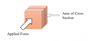
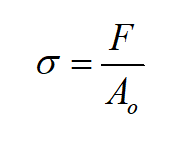
  • Instantaneous load or force applied per unit original area of cross-section (Before any deformation) is known as engineering stress.
  •  It is denoted by σ (sigma). SI unit of engineering stress is N/m2 or Pascal (Pa).

Engineering Stress= (Force Applied)/ (Original Area)

Strength of Material: Engineering Stress
Strength of Materials: Engineering Stress
Strength of Materials : Engineering Stress

Click Here! for more details

Classification of Stress

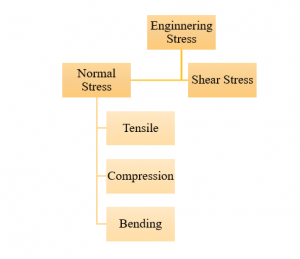
Generally following engineering stresses are classified in strength of materials studies.

Strength of Material : Classification of Engineering Stress
Strength of Materials : Classification of Stresses

Normal Stress

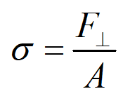
  • When the applied force is perpendicular to the given cross-section of the specimen (axial load), then the corresponding stress produced in the material is known as normal stress.
  •  Many times force applied on the surface is not uniform; in that case, we take an average of the applied force.

Normal Stress= (Perpendicular component of Applied Force)/ Area

Strength of Material: Normal Stress

Tensile Stress

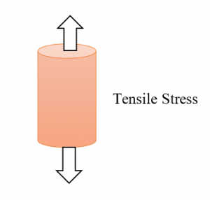
When the applied force is away from the material, then the Stress produced is known as tensile stress.

Strength of Material: Tensile Stress
Strength of Materials : Tensile Stress

Compressive Stress

When the applied force is in towards the object, then the Stress produced is known as compression stress.

Strength of material: Compressive Stress
Strength of Materials: Compressive Stress

Bending Stress

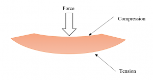
  • When force is applied on the beam-shaped material, the material’s top surface undergoes a compressive type of stress, and the bottom surface undergoes tension-type of Stress and middle of the beam remains neutral. Such stress is known as bending Stress.
  •  It is also known as flexural Stress.
Strength of Material: Bending Stress
Strength of Materials: Bending Stress

Shear Stress

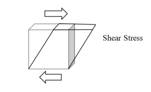
When the applied force is parallel to the area on which it is applied, the Stress is known as shear stress.

Strength of Material: Shear Stress
Strength of Materials : Shear Stress

Shear Stress Formula

Shear Stress= (Force imposed parallel to the upper and lower faces) / Area.

Strength of Material: Shear Stress

Tensile Stress vs Shear Stress

Tensile StressShear Stress
The applied force is perpendicular to the surface.The applied force is parallel to the surface.
It is denoted by σ.It is denoted by τ.

Combined Stress Equation

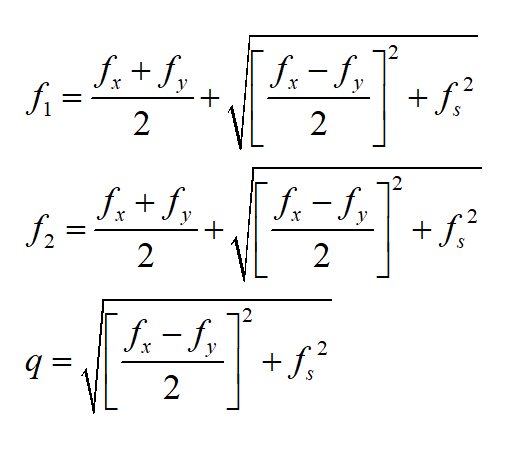
While studying strength of materials in real-life examples, we can have cases in which more than one type of Stress is acting on the material, in that case, we need to have an equation which can combine different type of stresses

Following is the equation which combines shear and tensile stresses.

Strength of Material: Combined Stress Equation

Where,

fx= tensile or compressive stress in the x-direction

fy= tensile or compressive stress in the y-direction

fs= shear stresses acting on the faces in x and y-direction

f1= maximum principle Stress

f2= minimum tensile Stress

q= maximum shear stress

Stress Concentration Factor

  • In the studies of Strength of Materials, many times the material on which we are applying Stress is not uniform. It may have some irregularities in its geometry or within the structure formed due to nicks, scratches holes, fillets, grooves, etc., which causes the concentration of stress to be very high at some point on the material known as stress concentration or stress riser/raiser.
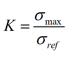
  • The degree of this concentration is expressed as the ratio of maximum Stress to reference Stress, where reference stress is total Stress within an element under the same loading conditions, without any concentration or discontinuity.

Stress Concentration Factor Formula:

Stress Concentration= maximum Stress / Reference Stress

Strength of Material: Stress Concentration Factor

Click Here! for more details

Factor of Safety

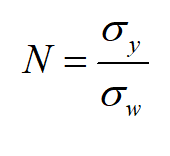
  • While studying strength of Materials, there are always some uncertainties in the measured values of stresses; therefore, the stress that we are going to consider for our use known as working stress (σw) is always less than the experimental value of stress. In most of the applications, we consider yield strength (σy).
  • Working Stress is determined by reducing the yield strength by a factor; that factor is known as the factor of safety. So, the factor of safety is a ratio of yield strength to working stress. Its symbol is N. It is a unitless quantity.

            Factor of Safety= Yield Strength/ Working Stress

Strength of Material: Factor of Safety

Engineering Strain

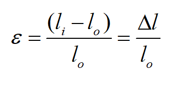
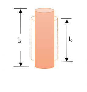
  • Change in length at some instant of the material per unit original length (Before any application of force) is known as engineering strain.
  •  It is denoted by ε (Epsilon) or γ (Gamma). It’s a unitless quantity.

              Engineering Strain= (Change in length)/ (Original Length)

Strength of Material: Engineering Strain Formula
Strength of Material: Engineering Strain
Strength of Materials : Engineering Strain

Poisson’s Ratio

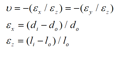
  • When tensile stress is applied to the material, there is elongation along the applied load axis and shortening along with perpendicular directions to the applied Stress. Thus, the strain produced in the applied stress direction is known as axial strain and the strain produced in the perpendicular direction the applied Stress is known as lateral strain or transverse strain.
  • The ratioof the lateral strain and axial strain is known as Poisson’s Ratio. It is denoted by ʋ (nu). It is a very important constant for a given material.

            Poisson’s Ratio= – (Lateral Strain/ Axial Strain)

Let the applied load is in z-direction and strain produced in that direction is εx  and  material is isotropic and homogeneous ( ) then Poisson’s ratio is

Strength of Material: Poisson's Ratio Formula
Strength of Material: Poisson's Ratio
Strength of Materials : Poisson’s Ratio

To learn in detail on Poisson’s Ratio Visit here

Stress-Strain Curve

  • Plotting of stress to strain gives a considerable number of properties of the material in strength of materials study.
  • The stress-strain curve is stress versus strain curve in which strain is on independent axis i.e., x-axis and stress is on dependent i.e. y-axis. It is an important characteristic of the material.
  • On the load application, two types of deformation occur in the material depending upon the strain value, first is elastic deformation and second is plastic deformation.
Strength of Material: Stress-Strain Curve
Strength of Materials: Stress-Strain Curve

True Stress-Strain Curve

It is a stress-strain curve in which true Stress is plotted against true strain. Both Stress and strain are based on instantaneous measurement. Hence, the instantaneous cross-section area is considered instead of original cross-section, and instantaneous length is considered instead of the original length.

Elastic Deformation

  • Elastic deformation is the deformation in which material regains its original shape on the removal of the force.
  • This region has a proportional limit, elastic limit, upper yield point and lower yield point.

Modulus of Elasticity | Hooke’s Law

  • When this type of deformation occurs, the strain in the metal piece is nearly proportional to the stress; therefore, this deformation occurs as a straight line in Stress versus strain plot except for some materials like grey cast iron, concrete and many polymers.
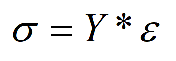
  • Stress is proportional to the strain through this relationship.
Strength of Material: Hooke's Law
  • This is known as Hooke’s Law, where Y the proportionality constant is known as Young’s Modulus or Modulus of Elasticity. It is also denoted by E. It is the slope of the stress-strain curve in the elastic limit. It is one of the most important law in the studies of strength of material.

Modulus of Elasticity Formula

Modulus of Elasticity Formula

Its value is slightly higher for ceramics than metals and value is slightly lower for polymers than metals. Or most structures are required to have deformation only in the elastic limit; therefore, this region is quite important.

Plastic Deformation

  • If the applied force is removed in this region, then the material does not regain its original shape.
  • The deformation in the material is permanent.
  • In this region, Hooke’s law is not valid.
  • This region has ultimate tensile strength of materials and breaking point.
  • There are some points on the curve around which type of deformation changes. These points are very important as they tell us about the limitations and ranges of material which are ultimately useful in material’s application.

Proportional Limit

  • It is the point in the curve up to which Stress is proportional to the strain.
  • When the material is stretched beyond the proportionality limit, stress is not proportional to the strain, but still, it shows elastic behaviour.

Elastic Limit

  • It is the point in the curve up to which material shows elastic behaviour.
  • After this point, plastic deformation in the material begins.
  • Beyond the elastic limit, Stress causes the material to flow or yield.

Yield Point

It is the point where yielding of the material occurs; hence plastic deformation of material begins from this point.

What is Yield Strength?

  • Stress corresponding to the yield point is known as yield strength—its resistance to its plastic deformation.
  • Many times it is not possible to locate it precisely. The elastic-plastic transition is well-defined and very abruptly, termed as yield point phenomenon.
  • Upper Yield Point: It is the point in the graph at which maximum load or Stress required to initiate the plastic deformation of the material.
  • Lower Yield Point: It is a point at which minimum Stress or load is required to maintain the material’s plastic behavior.
  • The upper yield point is unstable, but lower yield point is stable, so we use a lower yield point while designing the components.

Ultimate Strength Definition | Ultimate Stress Definition

  • After yielding, as plastic deformation continues, it reaches a maximum limit known as ultimate Stress or ultimate strength.
  • It is also known as Ultimate Tensile Strength (UTS) or tensile strength. It is the maximum stress that can be sustained by material in tension.
  • All deformation up to this point is uniform, but at this maximum stress, small narrowing of material begins to form, this phenomenon is termed as ‘necking’.

Rupture Point | Fracture Point | Breaking Point

  • Stress necessary to continue plastic deformation starts to decrease after ultimate strength and eventually breaks the material at a point known as rupture point or fracture point.
  • The stress of the material at rupture point is known as ‘rupture strength’.

Stress-Strain curve for Brittle material

Strength of Materials : Stress Strain Curve for Brittle Materials
Strength of Materials : Stress-Strain Curve for Brittle Material

Stress-Strain Curve for Ductile Material

Stress-Strain Curve for Ductile Material
Strength of Materials : Stress-Strain Curve Ductile Material

 Ref. – Stress-Strain

Important Questions and Answer related to Strength of Materials

What is engineering stress?

Instantaneous load or force applied per unit original area of cross-section (Before any application of force) is known as engineering stress.

It is denoted by σ (sigma). SI unit of engineering stress is N/m2 or Pascal (Pa).

What is Engineering Strain?

Change in length at some instant of the material per unit original length (Before any application of force) is known as engineering strain.

It is denoted by ε (Epsilon) or γ (Gamma). It’s a unitless quantity.

What is Tensile Stress?

When the applied force is away from the material, then the Stress produced is known as tensile stress.

Strength of Materials : Tensile Stress Figure
Strength of Materials : Tensile Stress

What is Compressive Stress?

When the applied force is in towards the object, then the Stress produced is known as compressive stress.

new image
Strength of Materials : Compressive Stress

What is Shear Stress?

When the applied force is parallel to the area on which it is applied, the Stress is known as shear stress.

What is Factor of Safety?

There are always some uncertainties in the measured values of stresses; therefore, the stress that we are going to consider for our use known as working Stress (σw) is always less than the experimental value of Stress. In most of the applications, we consider yield strength (σy).

Working Stress is determined by reducing the yield strength by a factor; that factor is known as the factor of safety. So, the factor of safety is a ratio of yield strength to working stress. Its symbol is N. It is a unitless quantity.

What is True Stress-Strain Curve?

It is a stress-strain curve in which true Stress is plotted against true strain. Both Stress and strain are based on instantaneous measurement hence instantaneous area of the cross-section is considered instead of original cross-section and instantaneous length is considered instead of the original length.

What is Breaking Point?

Stress necessary to continue plastic deformation starts to decrease after ultimate strength and eventually breaks the material at a point known as breaking point.

What is Ultimate Tensile Strength?

After yielding, as plastic deformation continues, it reaches a maximum limit known as ultimate Stress or ultimate strength, it is also known as Ultimate Tensile Strength (UTS)

What is Hooke’s Law? | Explain Hooke’s Law

When this type of deformation occurs, the strain in the metal piece is nearly proportional to the stress; therefore, this deformation occurs as a straight line in Stress versus strain plot except for some materials like grey cast iron, concrete and many polymers. Stress is proportional to the strain through this relationship.

e9 1

This is known as Hooke’s Law, where Y the proportionality constant is known as Young’s Modulus.

It is one of the most important law in the studies of Strength of Materials.

CONCLUSION

In this articles important terminology of strength of materials are explained in detailed such as engineering stress, strain, stress-strain curve for both ductile and brittle materials, young modulus, Poisson’s ratio etc. Strength of materials is also known as mechanics of materials.

To Learn more on mechanical engineering and Strength of Materials click here!

Permutations and Combinations: 11 Facts You Should Know

CodeCogsEqn 16 1

Permutations and Combinations

 Permutations and Combinations, this article will discuss the concept of determining, in addition to the direct calculation, the number of possible outcomes of a particular event or the number of set items, permutations and combinations that are the primary method of calculation in combinatorial analysis.

Common mistakes while learning Permutations and Combinations

There is always confusion amongst the student between permutations and combinations because both are related to the number of the arrangement of different objects and the number of the possible outcome of a particular event or number of ways to get an element from a set. The topic of permutation & combination with examples and the difference between them with justification will be discussed here.

A simple and handy technique to remember the difference between the permutations and combinations is: a permutation is related with the order means the position is important in permutation while the combination is not related with the order means the position is not important in combination.

Before the discussion of permutations and combinations, we require some prerequisites, which are frequently used.

 What is Factorial

          Factorial is the product of the positive integers from 1 to n (counting 1 and n) denoted by n! and read as n factorial is described as below

n! = 1.2.3.4… (n-2).(n-1).n = n.(n-1).(n-2)…3.2.1

nPr = n.(n-1).(n-2)…(nr+1) = n!/(n-r)!

Mind it 0!=1 

0! = 1

1! = 1

n! = n(n-l)!

e.g 3! = 3.2.1 = 6

4! = 4.3.2.1 = 24

5! = 5.4! = 5.24 = 120

Counting Methods (Principle of Multiplication and addition)

      Principle of addition: If no two events can happen at the same time, then one of the events can happen in

n1  + n2  + n3  +・ ・ ・.ways

      Principle of Multiplication: Considering that if the events occurred one after the other, then all the events can happen in the order indicated in:

n1.n2.n3ways

Example: If an Institute runs 7 different art courses, 3 different technical courses, and 4 different physical courses.

If a student wants to enroll one of each type of course then the number of ways would be

m=7.3.4=84

If a student wants to enroll just one of the courses, then the number of ways would be

n=7 + 3 + 4=14

What is Permutation

The different positioning of the objects are called Permutations, where the order of the arrangement matters. Any positioning of a set of n different objects in a given order is called a permutation of the object.

        Consider an example of the set of letters {P,Q,R,S}, then

  Some of the permutations of the four alphabets taken 4 at a glance are QSRP, SRQP and PRSQ

Any ordering of any r<=n of these particular objects in a specific order is called an “r-permutation” or “a permutation of the n objects taken r at a time.

Basically we like those number of such permutations without set down them.

Example of Permutation Formula

The number of permutations of n different objects taken r at a time will be indicated by

nPr = n. (n-1).(n-2)…(n-r+1) = n!/(nr)!

In mathematics this is denoted by different ways, some of them are mentioned below:

P(n,r), nPr,Pn,r ,or (n)r

EXAMPLE: Calculate the number m of permutations of six objects, say A, B, C, D, E, F taken three at a glance.

Solution:   Here n=6, r=3, m=?

nPr = n!/(n-r)!

m = 6P3 = 6!/(6-3)! = 6!/3! = 3!.4.5.6/3!= 4.5.6 = 120

So m=120

EXAMPLE: How many words can be generated by using 2 letters from the word “MATHS”?

Solution: Here n=5, r=2, m=?

nPr = n!/(n-r)!

m = 5P2 = 5!/(5-2)! = 5!/3! = 3!.4.5/3! = 4.5 = 20

so the required number of words are 20.

What do you understand by a Combination?

A combination for n different elements taken r at a time is any selection of r-th elements where orders are not being considered. Such a selection is called an r-combination. In brief, a Combination is a selection in which the order of the objects selected is not important.

      The Combination gives the number of ways a particular set can be arranged, where the order of the arrangement does not matter.

 To understand the situation of Combination, consider the example

Twenty people arrive in a hall and everyone shakes hand with all the others. How can we get the number of handshakes?  “A” shaking hands with B and B with A will not be two different handshakes. Here, the order of handshake is not important. The number of handshakes will be the combinations of 20 different things taken 2 at a time.

Combination Formula with a simple example

       The number of such combinations will be denoted by

CodeCogsEqn

Sometimes it is also denoted by C(n,r), nCr , Cn,r or Crn

Example: A class contains 10 students with 6 men and 4 women. Find the number n of ways to choose a 4-member committee among those students.

This is related to combinations, not permutations, since order is not an important factor in a committee. There are “10 choose 4” such committees. That is:

gif

here n=10, r= 4

CodeCogsEqn 15

so in 210 ways we can choose such 4-member committee.

Example: A container has 6 blue balls and 8 red balls. Identify the number of ways two balls of any of the colors can be drawn from the container.

Here possibly “14 choose 2” ways for selecting 2 of the 14 balls. Thus:

CodeCogsEqn 16

Here n=14 , r=2

gif.latex?%5E%7B14%7DC %7B2%7D%20%3D%20%5Cbinom%7B14%7D%7B2%7D%20%3D%20%5Cfrac%7B14%21%7D%7B2%21%2814 2%29%21%7D%20%3D%20%5Cfrac%7B14.13.12.%21%7D%7B2.1

so in 91 ways two balls can be drawn of any color.

Difference between Permutation and Combination

The difference between permutation vs combination is briefly given here

Permutation Combination
Order is Important Order is not Important
Order counts Order does not count
Used for arrangements like electing president, vice president, and treasurer Used for selection like selecting teams and committee without positions
For electing first, second and third specific positions For selecting any three random
For arranging the cards or balls with position and color For selecting any color and position
Difference between Permutations and Combinations

Where to apply Permutations and Combinations

  This is the important step that should be kept in mind that whenever the situation is for arrangement, ordering and uniqueness we have to use Permutation and whenever the situation is  for selection, choosing, picking and combination without the concern of order we have to use Combination. If you keep these basics in your mind there will be no confusion “what to use and what not” whenever a question arises.

Use of Permutations and Combinations in real life with examples

In real life permutation and the combination is used in almost everywhere because we know that in real life there would be a situation when order is important and somewhere order is not important, in those situations we have to use the corresponding method.

For example

Find the number N of teams of 11 with a given captain that can be selected from 26 players.

Frequently Asked Questions – FAQs

What is factorial?

The product of the positive integers from  1 to n (including 1 & n )

n! = 1.2.3… (n-2). (n-1). n

What is a permutation?

The different ordering of the objects are called Permutations

What is a Combination?

     The Combination provides the number of ways a specific set can be set out, where the order of the arrangement does not matter.

Application of permutations and combinations in practical life

A Permutation is used for arrangement or selection of lists where the order is important, and Combination is used for selection or choice where the order is not important.

Permutation formula

nPr = n!/(n-r)!

Combination formula

CodeCogsEqn 16 1

Is there any relation between permutations and Combinations?

Yes,

nCr = nPr/r!

Can we use Permutations and combinations in real life?

Yes,

In the arrangement of words, alphabets, numbers, positions and colours etc. where the order is important permutation will be used

In the selection of committee, teams, menu, and subjects etc where the order is not important combination will be used.

   The brief information about permutations and combinations with basic formula is given read twice or thrice till you get the idea about the concept, in consecutive articles we will discuss in detail the different results and formulae with suitable examples of permutations and combinations. If you want further study go through:

For more Topics on Mathematics, please follow this link.

References:

1.   SCHAUM’S OUTLINE OF Theory and Problems of DISCRETE MATHEMATICS

2.   https://en.wikipedia.org/wiki/Permutation

3.   https://en.wikipedia.org/wiki/Combination

4.   https://in.bgu.ac.il/

5.   https://www.cs.bgu.ac.il/

39 Important VLSI, VHDL & Verilog Interview Q&A

IMG24 1024x398 1

VLSI, VHDL, Verilog Interview Questions

1. Give the full term of VHDL.

  1. Very High Definition Language
  2. Very High Speed Integration Hardware Description Language
  3. Very High Description Language
  4. Very High Speed Scaling Hardware Describing Language

Ans: 2) Very High Speed Integration Hardware Description Language

For basic VHDL Tutorials, Click Here!

2. What is the number of Metal Oxide Filed Effect Transistors are needed to construct a Bi-complementary metal Oxide Semiconductor NOR gate which have two input?

  1. 5 MOSFETs
  2. 6 MOSFETs
  3. 7 MOSFETs
  4. 8 MOSFETs

Ans: 3) 7 MOSFETs

“How a Logic gate is designed in VLSI?” Find the answer here!

3. What is the effect of ‘Delay’ if the power supply voltage gets increased?

  1. Increases
  2. Decreases
  3. Remains the same
  4. Delay has nothing o do with power supply.

Ans: 2) Decreases

4. Which is true about VLSI design?

  1. VLSI is a sequential process which has feedback loops.
  2. VLSI is a parallel process which has no feedback loops.
  3. VLSI is both sequential and parallel process that has feedback loops.
  4. VLSI is a sequential process which has no feedback loops.

Ans: 3) VLSI is both sequential and parallel process that has feedback loops.

For more details about Verilog Interview Questions and other topic like VLSI Design, Check this!

5. What is the use of CAD tools in VLSI design?

  1. It automates the VLSI design.
  2. It reduces the design cycle time.
  3. It reduces the chance of errors.
  4. All of the above.

Ans: 4) All of the above.

6. Which type of product is more suitable for FPGA based Design?

  1. Large scale product development.
  2. High Speed applications.
  3. Prototype development.
  4. Low power applications.

Ans: 3) Prototype development.

What is Verilog? What is system Verilog? and other Verilog Interview Questions and Answers are here!

7. What is the relation between interconnect delay and gate delay?

  1. The Relation is technology dependent.
  2. Gate delay always more than interconnect delay.
  3. Interconnect delay always more than the gate delay.
  4. They are same.

Ans: 1) The relation is technology dependent.

8. State True or False

Statement: For a Y chart, the details of design information increases when moved from the centre to the periphery.

  1. True
  2. False

Ans: (2). False

9. Why a short channel device is preferred?

  1. It is easier for fabrication.
  2. It has lower power consumption.
  3. It has high speed.
  4. It has better output characteristics.

Ans: 3) It has high speed.

10. Where does the subthreshold operation of MOSFET find applications?

  1. Memories.
  2. Charge coupled devices.
  3. Biomedical applications.
  4. None of the above.

Ans: 3) Biomedical applications.

IMG24

Make your First VHDL Project!

Click Here!

VLSI, VHDL, Verilog Interview Questions, Image – 1

11. What is the relation between the ON-resistance of MOSFET and gate to source voltage (Vgs)?

  1. ON-resistance linearly increases with Vgs.
  2. ON-resistance linearly decreases with Vgs.
  3. ON-resistance exponentially increases with Vgs.
  4. ON-resistance non-linearly decreases with Vgs.

Ans: 4) ON-resistance non-linearly decreases with Vgs.

12. What is the threshold voltage of an EMOSFET?

  1. Equal to 0 V.
  2. Less than 0 V.
  3. Greater than 0 V.
  4. None of the above.

Ans: 3) Greater than 0 V.

13. Find the odd one out.

  1. Channel length modulation
  2. Subthreshold Conduction
  3. Hot carrier effect.
  4. Body Effect

Ans: 4) Body effect. (All the other options are 2nd order effect).

14. How does doping density change for constant voltage scaling?

  1. Increases by a factor of s
  2. Increases by a factor of s2.
  3. Decreases by a factor for s.
  4. Decreases by a factor for s2.

Ans: 2) Increases by a factor of s2.

15. How does power dissipation occur for full scaling?

  1. Increases by a factor of s
  2. Increases by a factor of s2.
  3. Decreases by a factor for s.
  4. Decreases by a factor for s2.

Ans: 3) Decreases by a factor of s2.

16. How does power dissipation occur for constant voltage scaling?

  1. Increases by a factor of s
  2. Increases by a factor of s2.
  3. Decreases by a factor for s.
  4. Decreases by a factor for s2.

Ans: 1) Increases by a factor of s.

17. What is the main advantage of depletion load NMOSFET inverter over EMOSFET load?

  1. Less power dissipation
  2. Easier fabrication process
  3. Sharper Vtc transitions and better noise margins.
  4. None of the above.

Ans: 3) Sharper Vtc transitions and better noise margin.

18. Why is polysilicon used for the gate in MOSFET?

  1. Because it is a semi-metal.
  2. Because it has lattice matching with Silicone
  3. Because it is easier to fabricate.
  4. None of the above.

Ans: 2) Because it has lattice matching with silicone.

19. State True or False

Statement: In full scaling, the magnitude of the electric field is constant.

  1. True
  2. False

Solution: (1). True

20. Which of the given statement is true regarding a MOSFET inverter?

  1. One PMOSFET and one resistor are needed to implement a MOSFET inverter.
  2. One NMOSFET and one resistor are needed to implement a MOSFET inverter.
  3. Two PMOSFETs.
  4. Two NMOSFETs.

Ans: 2) One NMOSFET and one resistor is needed to implement a MOSFET inverter.

Image 23 1

Build your first Verilog project!

Click here!

VLSI, VHDL, Verilog Interview Questions, Image – 2

21. On which factors, the power dissipation of a CMOS inverter depends?

  1. Supplied Voltage.
  2. NMOSFET’s channel width.
  3. PMOSFET’s channel width.
  4. All of the above.

Ans: 1) Supplied Voltage

22. State True or False

Statement: The PMOS transistors act as Pull-up network in a CMOS inverter.

  1. True
  2. False

Solution: (1). True

23. Which of the following effect has no contribution to deviate the ideal situation of a current mirror circuit?

  1. DIBL effects.
  2. Threshold offset between two transistors
  3. Channel length modulation
  4. Imperfect geometrical matching.

Ans: 1) DIBL effects.

24. What does the ASIC cell library contain?

  1. The physical layout of the cells
  2. Routing model of the cells
  3. Timing model of the cells
  4. All of the above.

Ans: 1) Physical layout of the cells.

25. Why does lowest propagation delay occur through a gate?

  1. Due to – strong transistor, high temperature, high voltage.
  2. Due to – strong transistor, low temperature, high voltage.
  3. Due to – Weak transistor, high temperature, high voltage.
  4. Due to – weak transistor, low temperature, low voltage.

Ans: 3) Due to – Weak transistor, high temperature, high voltage.

26. Which of the following is true about VLSI logic design?

  1. VLSI minimizes the area and delay
  2. VLSI minimizes the area at the cost of delay
  3. VLSI maximizes speed by decreasing area
  4. VLSI minimizes delay by reducing the area

Ans: 2) VLSI minimizes the area at the cost of delay.

27. What is a hard macro?

  1. Flexible Block
  2. Fixed Block
  3. Flexible block with a fixed aspect ratio
  4. Flexible block with a flexible aspect ratio

Ans: 2) Fixed Block

28. State True or False

Statement: The full form of SPICE is – Simulation Program with Integrated Circuit Emphasis.

  1. True
  2. False

Solution: (1). True

29. What is the equivalent circuit for CMOS comparator?

  1. Uncompensated CMOS OPAMP.
  2. Compensated CMOS OPAMP.
  3. Partially Compensated CMOS OPAMP.
  4. None of the above is true.

Ans: 1) Uncompensated CMOS OPAMP.

30. What is the relation between the equivalent resistance of a switched capacitor and the clock frequency?

  1. The resistance is proportional to clock frequency.
  2. The resistance is inversely proportional to clock frequency.
  3. The resistance is proportional to the square of the clock frequency.
  4. The resistance is inversely proportional to the square of the clock frequency.

Ans: 2) The resistance is inversely proportional to clock frequency.

VLSi 1

30 Most important and frequently asked VLSI Interview Questions! Click Here!

VLSI, VHDL, Verilog Interview Questions, Image – 3

31. What is the relation between the equivalent resistance of a switched capacitor and the capacitance?

  1. The resistance is proportional to the capacitance.
  2. The resistance is inversely proportional to the capacitance.
  3. The resistance is proportional to the square of the capacitance.
  4. The resistance is inversely proportional to the square of the capacitance.

Ans: 2) The resistance is inversely proportional to the capacitance.

32. What is the condition for domination by Diffusion Current?

  1. Strong Inversion
  2. Weak Inversion
  3. Both Strong and weak inversion.
  4. Cannot be determined.

Ans: 2) Weak Inversion.

33. What is the condition for domination by Drift Current?

  1. Strong Inversion
  2. Weak Inversion
  3. Both Strong and weak inversion.
  4. Cannot be determined.

Ans: 1) Strong Inversion.

34. State True or False

Statement: In the cascode current mirror, the output resistance is increased.

  1. True
  2. False

Solution: (1). True

35. State True or False

Statement: A current mirror circuit can be used as a current amplifier by increasing the (W/L) ratios of the mirrored and source MOSFET

  1. True
  2. False

Solution: (1). True

36. Which connections of NMOS in PDN, help to realize the AND terms?

  1. Cascade Connection
  2. Anti – parallel Connections
  3. Series Connections
  4. Parallel Connections

Ans: 3) Series Connections

37. Which type of transistor can pass logic-high value perfectly, but not the logic-low value?

  1. NMOSFET
  2. PMOSFET
  3. CMOS
  4. None of the above

Ans: 2) PMOSFET

38. What is the minimum number of transistors needed to design an XOR gate?

  1. Three
  2. Four
  3. Five
  4. Six

Ans: 4) Six

39. Which type of logic design provides the minimum propagation delay?

  1. Emitter Coupled Logic
  2. Transistor Transistor Logic
  3. Register Transistor Logic
  4. Diode Transistor Logic

Ans: 1) Emitter Coupled Logic

40. State True or False

Statement: Dynamic CMOS logic operates using two non-overlapping clock pulses.

  1. True
  2. False

Solution: (2). False.

For more VLSI related topic and Verilog interview questions click here

Verilog HDL Using Xilinx: 17 Important Steps You Should Know

INST 1 1024x576 1 300x169 1

Topics for Discussion

A. Xilinx

B. Prerequisites for Verilog HDL Using Xilinx

C. Xilinx Installation process

D. Creating your first Verilog project with XILINX

XILINX

Xilinx is a USA based tech-company which provides programmable logic devices. We will use Xilinx’s software “ISE 14.7 Simulator to implement Verilog designs. Xilinx is also used for VHDL implementations. Though some of the coding structure of Verilog is same as VHDL, there are fundamental differences between them.

First of all learn Verilog! Click Here!

Prerequisites for Verilog using Xilinx

Before getting started with Verilog with Xilinx, there are some prerequisites for an user. They are listed below.

  • Must have some knowledge of digital electronics. At least bits of knowledge of basic logic gates and sequential circuits are required.
  • An uninterrupted internet connection is a must.
  • A healthy amount of free memory is required to run the software smoothly. At least 20 GB space is needed in your machine.
  • Create an account on Xilinx’s website with an accessible email-id. The license will be mailed in that email-id.
  • We are demonstrating this tutorial for windows only.   
What is VHDL? What is the difference between Verilog & VHDL?

Xilinx Installation Process

  • Step 1: Download the software from the internet. The link to download Xilinx is given below –

(It is a 6GB ZIP file, ensure internet connection and space) The link for windows –

https://www.xilinx.com/member/forms/download/xef.html?filename=Xilinx_ISE_DS_Win_14.7_1015_1.tar

There are other downloadable options available. You can choose according to your requirement and choice from the below given link.

https://www.xilinx.com/support/download/index.html/content/xilinx/en/downloadNav/vivado-design-tools/archive-ise.html

  • Step 2: Unzip the file. To unzip the file, right-click on the file, and there will be an option to extract all. After the extraction, the file name should be – ‘Xilinx_ISE_DS_Win_14.7_1015.1”.

Point to be noted – Both the download and extraction will need a lot of time depending upon internet speed and storage availability. The installation will require a lot of time too. So, don’t panic, be patient.

  • Step 3: Open the extracted file. There is a file named – ‘xsetup’. Double click on that file. It will start the installation.
INST 1 1024x576 1
Choose the ‘xsetup’ file, Verilog HDL
  1. There will be another pop-up, choose the ‘ISE WebPACK’ option to continue.
INST 2 1
Choose the ISE WebPack, Verilog HDL

It will start the final installation process.

  • Step 4: After the software gets installed in your PC, some tasks must be performed. Do these tasks carefully. Also, update the license from Xilinx. Those steps are given in the previous article; please check it out before we start with our first Verilog Project. The link is given below.

https://lambdageeks.com/vhdl-process-xilinx-guide/

Creating your first Verilog project with XILINX

We will first implement a simple AND gate model using XILINX. The logical representation of AND gate is Y = AB; A and B are the two inputs, while Y is the output. The truth table is given below.

ABY =AB
000
010
100
111
Verilog HDL – AND gate truth table
  • Step 1: Open the project navigator by double clicking the icon on the desktop.
  • Step 2: Go to ‘File’ and then ‘New Project’. File -> New Project
Image 1 1
File -> New Project, Verilog HDL, Image 1
  • Step 3: Type a name for your project and select the storage location. It is advised not to use basic logic gate names as they are reversed keywords. Also, don’t forget to copy the name of your project; it will help your letter. Click on the ‘Next’ button to proceed.
IMAGE 2 1
Type a Name for the Project, and Choose Next, Verilog HDL Image – 2
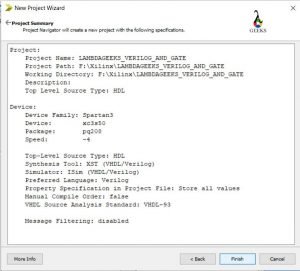
  • Step 4: Now, you have to set up a few things. Be careful while setting up all these things. Any mistake will lead to failure in the long-term result.
  • Property Name: Value
  • Evaluation Development Board: None Specified
  • Product Category: All
  • Family: Spartan3
  • Device: XC3S50
  • Package: PQ208
  • Speed: -4
  • Top Source Type: HDL
  • Synthesis Tool: XST (VHDL/Verilog)
  • Simulator: lSim (VHDL/Verilog)
  • Preferred Language: Verilog
  • Property Specification in Project File: Store all values
  • Manual Compile Order: Leave the checkbox, don’t click on it.
  • VHDL Source Analysis Standard: VHDL-93
  • Enable Message Filtering:  Leave the checkbox, don’t click on it.

Click on ‘Next’ to proceed.

Image 3 1
Do the setup carefully, Change the preferred language to ‘Verilog’, Verilog HDL Image – 3
  • Step 5: Now, click on ‘Finish; for the next pop-up.
Image 4 1
Click on ‘Finish’, Verilog HDL, Image – 4
  • Step 6: A new window will be opened up in the ISE simulator. Inside the design tab at the left corner, and under the Hierarchy bar, the model will have appeared. Move your cursor on the folder just below the named model.

Then right-click on the folder (in our case the name of the folder is – ‘xc3s50-4pq208’). Then, select the new source.

Verilog HDL
Right Click and choose the ‘New Source’, Image – 5
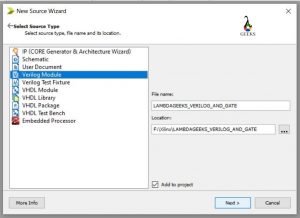
  • Step 7: In the new window, choose the ‘Verilog Module’ and paste the same name you have copied in the step 3. You can also get that name from the location tab. Click on ‘Next’ to proceed.
Image 6 1
Choose Verilog Module, Image – 6
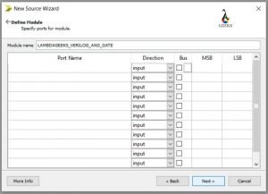
  • Step 8: The defining module will come up. But we will not define the ports now. Just click on ‘Next’.
Image 7 1
Click on NEXT, Verilog HDL, Image – 7
  • Step 9: Click on “Finish” for the next window pop-up.
Image 8 1
Click on ‘Finish’, Image – 8
  • Step 10: A code editor will be opened up.
    • Now change the project name written in the editor to “AND”. For our case, we change it from ‘LAMBDAGEEKS_VERILOG_AND_GATE’ to ‘AND’.
Image 9 1
Rename the module in the editor, Verilog HDL, Image – 9
  • Now write down the port declarations as follow.

module AND (

                        input I1, I2,

                        output O

                        );

endmodule

  • Now assign the AND gate in-between the input and output.

assign O = I1 & I2;

Image 10 1
Write down necessary Verilog code, Verilog HDL, Image – 10
  • Save the code.
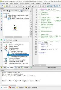
  • Step 11: Now, on the left side of the window, under the design bar, you can see a tab named “Process AND”.
    • Expand the ‘Synthesis – XST’ from there.
    • Double click on the ‘Check Syntax’. It will show a green tick, denoting success.
Image 11 693x1024 1
Complete the check syntax process, Verilog HDL, Image – 11
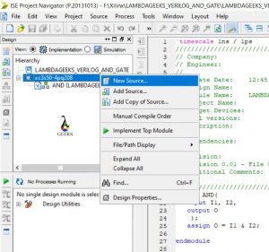
  • Step 12: Now again go back to the top-left section. Right-click  on the ‘xc3s50-4pq208’ file. Choose a new source from there.
Image 12 1
Add new source, Verilog HDL, Image – 12
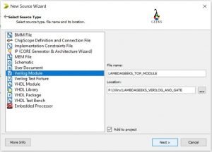
  • Step 13: Choose Verilog Module from the given list. Then put a file name. We put “LAMBDAGEEKS_TOP_MODULE” as the name. Click on the ‘Next’ to proceed.
Image 13 1
Choose Verilog Module, Verilog HDL, Image – 13
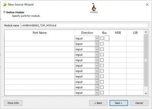
  1. A pop-up named ‘Define Module’ will come. Do not define anything here. Click on the ‘Next’.
Image 14 1
Click on Next, Verilog HDL, Image – 14
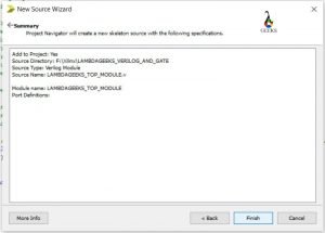
  • Click on ‘Finish’ for the next popped-up window.
Image 15 1
Click finish, Verilog HDL, Image – 15
  • Step 14: A code editor will be opened up. You can erase all the comment section from the code editor.
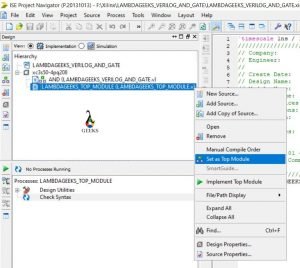
    • Now, check the Hierarchy Section at the top left. Right-click on the Module Name given by you. For our case, it is – ‘LAMBDAGEEKS_TOP_MODULE’.
    • Some options will come upon the right click. Choose the option – ‘Set as Top Module’.
Image 16 1
Select as Top Module, Verilog HDL, Image – 16
  • A window will pop-up. Click on ‘YES’ to continue.
Image 17 1
Click on Yes, Verilog HDL, Image – 17
  • Step 15: Now, we have to write some code using the code editor. It describes the input and output with the gate implementation. The following code is written for AND gate –

module LAMBDAGEEKS_TOP_MODULE(

            input I1, I2,

            output O

  );

            AND and1(I1,I2,O);

endmodule

Image 18 1
Write the corresponding Verilog Code, Verilog HDL, Image – 18
  • Step 16:  Now go to the left down part at ‘Process: LAMBDAGEEKS_TOP_MODULE’ section.
    • Now Expand the ‘Synthesis -XST’ part.
    • Double click on the ‘Check Syntax’. It will show a green tick denoting success after a few seconds.
    • Then, Double click on the ‘Synthesis – XST’ option. It will take a few seconds to show a green tick.
Image 19 1
Complete the check Syntax, Verilog HDL, Image – 19
  • Step 17:  View for RTL Schematic.
    • Double click on the ‘View RTL Schematic’ option.
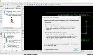
    • A window named – ‘Set RTL/ Tech Viewer behaves when it is initially invoked’ will pop up. Just click on the ‘OK’.
Image 20 1
Choose the second option, Verilog HDL, Image – 20
  • Now a window will be opened with a diagram.
Image 21 1024x576 1
Verilog RTL Schematic, Verilog HDL, Image – 21
  • Double click inside the box.
Image 22 1024x459 1
Verilog RTL Schematic, Verilog HDL, Image – 22
  • Now, double click inside the AND box.
Image 23 1024x466 1
Verilog RTL Schematic, Verilog HDL, Image – 23
  • Step 18: View for Technology Schema
    • Double click on the ‘View technology Schematic’ option.
    • A pop-up will come to click on the ‘OK’ option.
Image 24 1024x609 1
Technology Schema, Verilog HDL, Image – 24
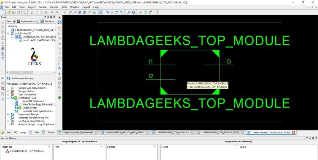
  • A new diagrammatic window opened up.
Image 25 1024x516 1
Verilog Technology Schema, Verilog HDL, Image – 25
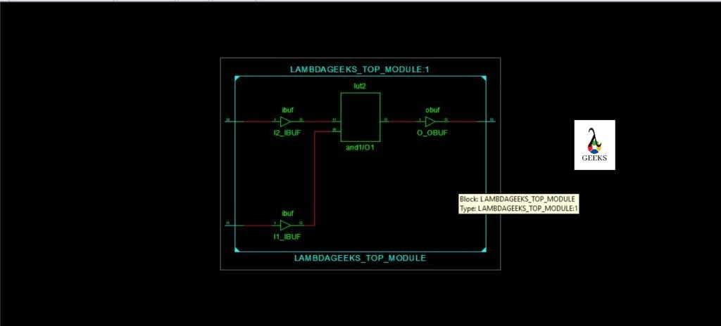
  •  Double Click inside the box of the diagram.
Image 26 1 1024x464 1
Verilog Technology Schema, Verilog HDL, Image – 26
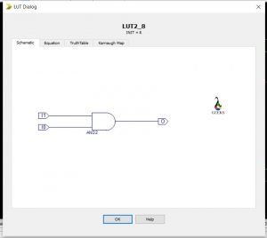
  • A box will be there named – ‘lut2’. Double click on that.

It will display several diagrams.

The schematic Diagram:

Image 27 1
Schematic Diagram
  • Click on the Equation to see the relation.
Image 28 1
Equation
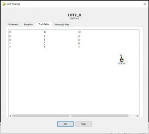
  • Click on the Truth table to find the truth table.
Image 29 1
Truth Table
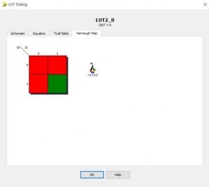
  • Click on the Karnaugh Map to find the Map.
Image 30 1
K- MAP of AND gate

Check out our other VLSI articles!

Verilog Tutorial: 5 Interesting Facts To Know

verilog tutorials 0

Verilog Tutorial : Points of Discussion

  • What is Verilog?
  • History and Standardization
  • Verilog Design
  • Verilog Modelling
  • Verilog Operators

For others topic related to Verilog Tutorial, Click Here!

What is Verilog?

Verilog is the combination of the terms “Verification” and “Logic”. It is hardware description language or a special type of programming language which describes the hardware implementations of digital system and circuits. It is a strongly typed language and points to be remembered that it is not a programming language.

For step-by-step VHDL Tutorial, Click Here!

History and Standardization of Verilog

Prabhu Goel, Chi-Lai Huang, Douglas Warmke and Phil Moorby developed the Verilog around the year 1983-1984. The first name was “Automated Integrated Design Systems” which was further renamed as “Gateway Design Automation” and was purchased by Cadence in the year 1990. Cadence is now the copyright owner of Verilog and the Verilog-XL.

Primarily, the use of Verilog was to define and to start the simulation. Later the popularity of the language raised a demand for more development, and it leads to the synthesis of the logic circuits.

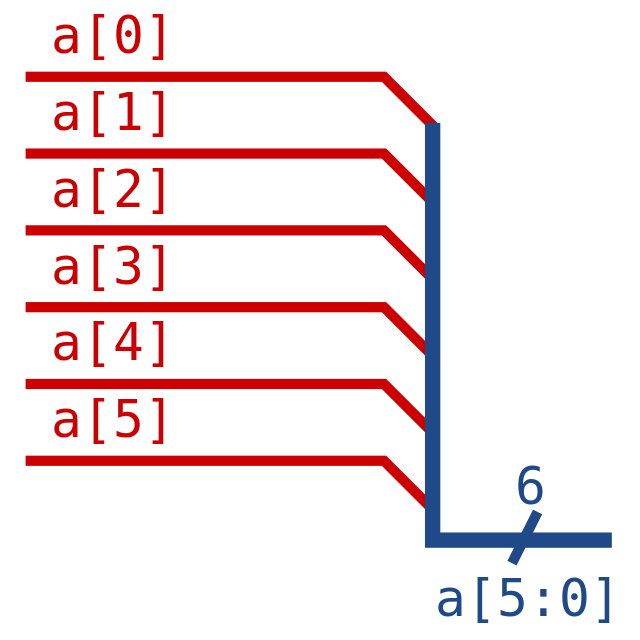
640px Verilog Bus.svg
Verilog Bus, Image Credit – InductiveloadVerilog Bus, marked as public domain, more details on Wikimedia Commons

Verilog Tutorial: Standardization

The popularity for VHDL forced cadence to publish the Verilog Language as open source. The first standardization of Verilog by IEEE was labelled as 1364-1995 and named as Verilog-95.

RevisionsUpdates
IEEE 1364 – 2001Verilog-2001. Supports signed variables and nest. Largely used by EDA packages.
IEEE 1364-2005Verilog 2005. Came up with little corrections and clarifications.
IEEE P1800-2005System Verilog.
IEEE 1800-2017Merger of SystemVerilog and Verilog. Known as SystemVerilog 2009.
IEEE Standardization of Verilog, Verilog Tutorial Table -1

Verilog Design

Verilog has two types of design methodologies. They are – Bottom-up approach & Top-down approach.

Bottom-up Approach: It is the conventional way of designing models. The planning is implemented at the gate level. Typical gates are used for implementations. This method opens up paths for different structural and ordered planning.

Top-down Approach: This approach has some advantages over the conventional one. Changes can be made easier here. Early testing is also possible.

Verilog Modelling

Verilog modelling has some design units. Let us discuss the primary components.

Verilog Code 1
Verilog Code for flip-flops

A. Module

A Verilog model comes up with port declarations, data type declarations, circuit functionality, timing specifications. A basic structure of the Module is given below.

module module_name (port_list);

<port_declarations>

<data_type_declarations>

<circuit_functionality>

<timing_specifications>

end module

  • Verilog is case sensitive.
  • Reserved keywords are written in lower cases.
  • A semicolon is used to terminate the statement.
  • The comment rule is same as C Programming Language.
  • Single line comment starts with “//”.

For example – //Example of a Verilog single line comment

  • Multiline comments start with – ‘ /*’  and ends with ‘*/’.

For example –

/* Example

Of Verilog multiple

Line comment*/

  • Timing specifications are used for the simulation process.

A module consists of a maximum of four levels of notion. The levels are defined below.

Behavioral: The highest level of notion. The anticipated design is planned at this level. Though, there is no thought for hardware implementations.

Dataflow: This level of Verilog Module describes the dataflow of the desired design. Hardware implementations of the dataflow through components are kept in mind while designing this level.

Image 26 1024x464 1
Dataflow Modelling, Verilog Tutorial

Gate: Logic gates are implemented in this Verilog module level. Interconnections are implemented between the gates.

Switch: The lowest level of notion. Switches, storage lumps are implemented. The interconnections are also designed between them.

B. Module Declarations

Module declarations start with ‘module’ keyword. It includes a port list (if exists).

Port types: There are three types of ports. The name and its functionality are given below.

  • input – input port
  • output – output port
  • inout – bi-directional port
Module Mixing 1
Verilog Code for Module Mixing, Verilog tutorial

Port Declarations: The general structure for port declarations is given below.

<port_type> <port_name>;

C. Data Types

There are several kinds of data types in Verilog.

 Net Data Type: This type of data describes the physical interrelate between flows.

Nets -> Functional Block: MUX -> Functional Blocks: Adders -> Nets

The below table will provide more details about Net Datatype.

TypeCharacterization
wireDescribes node or connections
triDescribes a tri-state node
supply0Represents Logic 0
suppy1Represents Logic 1
Net Data Types, Verilog Tutorial Table – 2
  •  Bus declarations: The general structure of bus declarations is given below.

<data_type> [Most Significant Bit (MSB): Least Significant Bit(LSB)] <signal_name>;

          <data_type> [Least Significant Bit(LSB): Most Significant Bit(MSB)] <signal_name>;

For example –

wire [3: 1] in;

Variable Data Type: This datatype describes the element to save a data for the time being.

There are many types of variable, supported by Verilog. Some of them are –

integer – 32 bits, Signed.

reg – any bit size, unsigned. To implement signed reg, use keyword – ‘reg signed’.

real, time, realtime – no support for synthesis.

D. Module Instantiation

After all the declarations, the module can be instantiated at a higher-level module with the help of some syntaxes. By instantiating modules, we can build designs with multiple levels of hierarchy. That will further help us to achieve simpler maintainability. Most of the modern designs have numerous layers of hierarchy.

The general format for instantiation is given below.

<componenet_name> #<delay> <instance_name> (port_list);

component name: It is the name of the module for the lower-level component.

delay: It is an optional choice. Delay introduces a delay throughout the component.

instance name: It is the exclusive name given by the designer for every individual instance.

port list: Port list gives the signal lists which will be connected to the component.

E. Simulation Component

After the designing process get completed, the testing process starts. This testing can be done using the stimulus block. Stimulus blocks are commonly known as a test bench.

Stimulus applications can be of two types. The primary design starts with the design block and directly drags the port signals into the design blocks.

The second design instantiates the stimulus block and the design block in a higher-level replica model. Interface is the communication link between the blocks.

Some Basic Verilog Concepts

Verilog Operators

Verilog has three fundamental operators for Verilog HDL. They are given below.

Unary Verilog operators : These types of Verilog operators come first of the operands.

For example: x = ~ y; Here ‘~’ is a unary operator

Binary Verilog operators : These types of Verilog operators come in-between two operands.

For example: x = y || z ; Here ‘||’ is a binary operator.

Ternary Verilog operators : These types of Verilog operators use two different operators to differentiates three operators.

For example: x = y?  z  : w; here ‘?’ and ‘:’ are ternary operators.

Verilog HDL’s categorical operators are – arithmetical, logical, relational, bitwise, shift, concatenation, and equality. Different types of Verilog operators and their symbols are given in the below table.

Type of OperatorSymbolOperationOperands needed
Arithmetic*MultiplicationTwo
Arithmetic/DivisionTwo
Arithmetic+AdditionTwo
ArithmeticSubtractionTwo
Arithmetic%ModulusTwo
Logical!negationOne
Logical&&ANDTwo
Logical||ORTwo
RelationalGreater thanTwo
RelationalLess thanTwo
Relational> =Greater than or equal toTwo
Relational< =Less than or equal toTwo
Equality==Equals toTwo
Equality! =Not equals toTwo
Equality===Case equalTwo
Equality! ==Case not equalTwo
Bitwise~NegationOne
Bitwise&Bitwise ANDTwo
Bitwise|Bitwise ORTwo
Bitwise^Bitwise XORTwo
Bitwise~^Bitwise XNORTwo
Reduction&Reduction ANDOne
Reduction~&Reduction NANDOne
Reduction|Reduction OROne
Reduction~|Reduction NOROne
Reduction^Reduction XOROne
Reduction^~Reduction XNOROne
Shift>> Right ShiftTwo
Shift<< Left ShiftTwo
Concatenation{ }ConcatenationCan be of any numbers
Replication{ { } }ReplicationCan be of any numbers
Conditional? :ConditionalThree
Verilog operators, Verilog Tutorial Table – 3

Verilog Operators has precedence also. Their Precedence is given in the below table.

OperatorSymbolsPrecedence
Unary Multiplication, Division, Modulus + ,-, !, ~ *, /, %Highest
Addition, Subtraction Shift+, – <<, >> 
Relational Equality<, <=, >, >= ==, !=, ===, !== 
Reduction     Logical&, ~& ^, ^~ |, ~| && || 
Conditional?:Lowest
Verilog Operator, Verilog tutorial table – 4

Verilog Number Specifications

Verilog numbers are of two types, sized numbers and unsized numbers.

Sized Verilog numbers: The general structure for representing sized numbers in Verilog HDL is given below.

<size>’<base_format><numbers>

For example – 8’b3456;

This is a sized Verilog number which describes that it is an 8-bit number and of binary type.

  • size: Size is the number of digits the main number has. Size is described using decimal values.
  • base_format: Base format suggests which type of number it would be. There are several types – binary (given by – ‘b’), decimal (given by – ‘d’), octal (given by – ‘o’), hexadecimal (given by – ‘h’). If there is no specification for base_format, then by default it is a decimal number.
  • numbers: The main number you want to put in.

Unsized Verilog numbers: These numbers do not require any specified size.

The general structure for representing unsized numbers in Verilog HDL is given below.

’<base_format><numbers>

For example – ’h3456;

This is an unsized Verilog number which describes that it is a hexadecimal number.

Negative Numbers: If you want to declare a number as a negative number, then put a minus symbol (-) before the number.

For example: – 345; it is a negative, unsized, decimal number.

Verilog Arrays

Arrays of integer, registers (reg), vectors ( of reg or net data types, several bit lengths) and time are possible in Verilog HDL. The basic declaration of arrays is shown below with an example.

integer matrix [0:3];

This means an array of seven values.

  • Verilog doesn’t allow any array for real variables.
  • Verilog HDL doesn’t support any multidimensional array.
  • Array elements can be retrieved using – <array_name>[<position_of_the_element>]

For others topic related to Verilog Tutorial, Click Here!

For step-by-step Verilog Tutorial using Xilinx, Check our next article!

Multiplexing: 7 Important Facts You Should Know

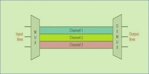
multiplexing 300x198 1

CONTENTS

  • What is Multiplexing ?
  • What are the types of Multiplexing ?
  • Time Division Multiplexing (TDM)
  • Descriptions of TDM
  • Frequency Division Multiplexing (FDM)
  • Descriptions of FDM
  • TDM vs FDM

What is Multiplexing ?

Define Multiplexing:

“Multiplexing is a method where many message signs are assembled into a composite signal for the purpose of transmission through a communication channel”.

These signals are transmitted through one communication channel. The signals have to be specified so that they do not interfere with one another, and they have to be separated in the receiver end again to recreate the original signal.

Multiplexing
Multiplexing, Image Credit – The AnomeMultiplexing diagramCC BY-SA 3.0

Multiplexing Techniques

It is of two types as follows:

  1. Time Division Multiplexing (TDM)
  2. Frequency Division Multiplexing (FDM)

Time Division Multiplexing:

What is TDM?

Time Division Multiplexing (TDM) is a technique in which a number of signals are made to pass through a common channel at different time slots.

Time Division Multiplexing (TDM)
Image credit: Tony R. Kuphaldt, Telephony multiplexer systemCC BY 1.0

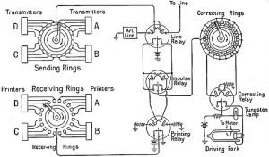
Diagram of TDM:

510px EB1922 Telegraph Simplified Terminal Circuit of Multiplex Printer System
Time Division Multiplexing in Telegraph, Image Credit – William Noble, EB1922 Telegraph – Simplified Terminal Circuit of Multiplex Printer System, marked as public domain, more details on Wikimedia Commons

Here, the TDM technique is employed to the three analog resources that are multiplexed through a PCM system. In practice, a digital switch is utilized for its sampler. This fs = 1/Ts represents the frequency of spinning to its sampler; also fs fits the Nyquist rate for its analog sources with the maximum selective bandwidth. In the certain process where the bandwidth of these is different, the bigger bandwidth resources could be linked to many switch places onto the sampler side to be usually sampled more than the shorter bandwidth input signal.

In the receiver, the sampler needs to be connected with the processed waveform, so the PAM samples corresponding to input one will show up on the channel just only output signal. This is known as ‘frame synchronization’. Lpf has been utilized to rebuild the analogue signals in the PAM samples. ISI resulting in bad channel filtering may induce PCM samples from one communication channel to look on other station, and frame synchronization condition has been maintained. The feedthrough of a one specific communication channel into the other channel is known as cross-talk.

Advantages and Disadvantages of TDM:

Advantages of TDM

  • Usually, TDM is more flexible than FDM.
  • The circuit design of TDM is not complicated.
  • In TDM, less cross-talk has occurred.
  • Channel bandwidth length is longer.

Disadvantages of TDM

  • Frequency Division Multiplexing process has no need of synchronization.
  • Implementation can be complex.

Applications of TDM

  • In ISDN (integrated service digital network), TDM is used.
  • In PSTN (public switched telephone network), TDM is used.
  • In a telephone system, TDM is widely used.
  • TDM is used in telephone wire lines.

Frequency Division Multiplexing:

What is FDM?

Frequency Division Multiplexing is a mechanism of signal transmission in which sharing the available bandwidth of a communication channel occurs among the signals to be transmitted.

In general, FDM schemes are utilized for the analog signal applications.

Diagram of Frequency division Multiplexing:

FDM
Frequency division Multiplexing

FDM is a method of transmitting many messages concurrently through a wideband by modulating the message signals on a few subcarriers and forming a composite baseband signal. This mixed signal is dependent on the quantity of those controlled subcarriers. This mixed signal could then be modulated by AM, DSB, SSB, PM, FM, as the primary types. The type of modulation used in the subcarriers may differ, and also the type used in carrier signal could also differ.

On the other hand, the mixed signal range should consist of inputs signal that should not possess overlapping spectra; otherwise, cross-talk will happen involving the receiver end’s message signals. The mix baseband signal subsequently modulates the transmitter to create the FDM signal sent across the wideband channel.

This FDM collected and demodulated to recreate the combination baseband signal filtered through filters and modulated subcarriers. The sub-carrier has to be demodulated to reproduce the message signals such as m1(t), m2(t) etc.

A speaker with a traditional monaural FM receiver may listen to that the audio sound (composed of the remaining – and the right-channel sound ). By comparison, a speaker with a stereo recipient will get the left-channel sound on the left speaker and the right-channel sound on the ideal speaker. The gap sound is used to govern a 38-kHz DSB-SC sign. Even a 19-kHz pilot tone has been mixed into the mix baseband signal mb(t) to supply a reference sign for coherent subcarrier demodulation in receiver end. As we all know, this program can be used with present FM monaural recipients.

Advantages and Disadvantages of FDM:

Advantages of FDM

· Between the transmitter and receiver, unlike TDM, FDM does not need any synchronization.

· Through FDM, a large number of signals can be transmitted simultaneously.

· Slow, narrowband fading can only affect one single channel.

· Demodulation of FDM is much easier comparatively than TDM.

Disadvantages of FDM

  • This suffers from cross-talk problem.
  • In this type Communication channel must have a large bandwidth.
  • In the technique, its channels get affected due to band fading.
  • In FDM intermodulation distortion takes place.

Applications of FDM

For more electronics related article click here

Perfecto Tutorial – An Excellent Perfecto Selenium Integration Tutorial Part 2

Perfecto Selenium Integration Access Perfecto Cloud 300x143 1

The scope of software testing is leading the IT industries now to ensure the quality of the product. Apart from regular web application testing, the scope for mobile testing is also rapidly increasing. The mobile devices can be tested either manually or through the mobile automation tools. Many mobile test automation tools are available in the market which provides mobile labs and the automation capabilities as well. The well known tools are Perfecto, SeeTest, Mobile Lab, etc. 

Perfecto Tutorial – Table of Content

Perfecto Tutorial 1# Install Selenium Setup for Web Automation

Perfecto Tutorial 2# Perfecto Selenium Integration for Mobile Automation

Perfecto Tutorial 3# Import Sample Project for Perfecto Automation

Through this, “Selenium for Perfecto” article, we will provides a complete and detailed overview of Perfecto Selenium Integration using Selenium WebDriver (Java). Also, we will execute a sample project for Perfecto automation with the help of Perfecto mobile lab and automation capabilities.

Perfecto Selenium Integration for Mobile Automation

In this section, we will explain the step by step approach to execute selenium webdriver test cases using the Perfecto mobile lab and automation capabilities. The pre-requisites assumptions to start with this article, are mentioned below –

  • Basic knowledge in Selenium WebDriver.
  • Developed a Selenium test case which will be used here.
  • New to the Perfecto.

Configuration details for Perfecto Automation:

Here we will update the pom.xml file with the necessary Perfecto dependencies and edit the codes from Step 1 to add them in the security data, the Perfecto cloud name, driver details, smart test data update.

The modified code is called PerfectoSelenium.java. The below process walks the users through the configuration.

  • Copy the dependencies
  • Supply the security token
  • Select a device
  • Supply the URL to connect to the Perfecto cloud
  • Create an instance of the reporting client
  • Execute the test

Step1# Accessing Perfecto Cloud: 

  • Register for the first time user for two weeks of the free trial from the perfecto trial license web.
  • Log in with the Perfecto cloud using the above free trial user.

Step2# Capture Security Token from Perfecto Cloud:

The security token is an encrypted version of long string which will be used later to connect the Perfecto mobile lab from third-party tools like Selenium WebDriver. Steps to capture the security token are mentioned below –

First, click on user name which is displayed in the right top corner and click on “My Security Token” link from user menu to open “My Security Token” popup.

Here, we need to click on “GENERATE SECURITY TOKEN” button and copy the generated security token.

Perfecto Selenium Integration - Perfecto Security Token
Perfecto Selenium Integration – Perfecto Security Token

Step3# Select a Device and get the Capabilities:

Capabilities are used to define the mobile devices which will be accessed from the Perfecto cloud. The structure for defining the capabilities are look like below –

DesiredCapabilities capabilitiesSample = new DesiredCapabilities(webBrowserName, “”, Platform.ANY);

capabilitiesSample.setCapability(“testPlatformName”, “Android”);

Here, “platformName” capability is used to define the platform of the mobile OS. To find the source code for the desire capabilities of the mobile android devices, we need to open the Perfecto Cloud UI with Manual Testing view. The source code of capabilities, can be copied to our selenium test case. The steps to follow for capturing the desire capabilities through the perfecto mobile cloud are mentioned below –

  • Click on Open Device option which is available under the Manual Testing section. This section is located in Perfecto Landing page.
  • On the Manual Testing view, select a device to proceed next.
  • Now click to open the Capabilities tab which is available in the details pane. The details pan will be available after selection of the device only.
  • All the capabilities will be displayed here. We can copy either all or selected capabilities based on the requirement.
Perfecto Selenium Integration - Perfecto Mobile Capabilities
Perfecto Selenium Integration – Perfecto Mobile Capabilities

Step4# URL to Connect Perfecto as Appium Server:

The structure of the URL for perfecto cloud will be looks like below – 

https://<<Cloud Name>>.perfectomobile.com/nexperience/perfectomobile/wd/hub

If the URL to access the Perfecto cloud manually is “https://testingcloud.app.perfectomobile.com/lab/devices” then the cloud name will be testingcloud.

Step5# Reporting Client Instance Creation:

The best way to run our test in Perfecto, the first step is to crate an instance with the reference of ReportingClient class i.e., the smart reporting client. It will help us to analyze the report after the test execution. The reporting client is used to collect the basic information of the test. Later, this information will be send to the Smart Reporting system. 

In the sample project(Utils.java), we have shown about the usage of the ReportiumClientFactoryclass’ createPerfectoReportiumClient() method. The instance of PerfectoExecutionContext class provides the link to the factory class.

withWebDriver() – With the help of this method, the link for the driver instance are supplied.

build() – This method is used to create the instance of the context object which will be supplied to the createPerfectoReportiumClient() method for ReportiumClient instance creation.

The main purpose of this reporting is to analyze the test result from the Perfecto Cloud.

Perfecto Selenium Integration - Reporting Client Instance
Perfecto Selenium Integration – Reporting Client Instance

Sample Project to Demonstrate the Perfecto Automation Approach in Mobile Devices

Manual Test Scenario:

  1. Login to the perfecto mobile cloud with valid user credential.
  2. Select any available device.
  3. Open the setting app.
  4. Click on sub-menu contains text as “data usage”.
  5. Verify that “Data Saver” submenu will be displayed.

Basic Information Collected: As pert of test automation, we have collected the Information such as cloud name, security token, capabilities, app package/activity name, captures the object’s property, etc.

Download codes for a sample project: Please click here to download codes for Sample Project. In this sample project, the basic codes are available for Local Appium, Local Selenium, Perfecto Appium and Perfecto Selenium. In this article, we will execute the java test code for Perfecto Appium.

Steps to Prepare the Test for Execution:

Step 1# Import the Sample Project into Eclipse Workspace, which was downloaded previously. This project can be imported through navigation “File->Open Projects from File System” available in Eclipse IDE.

Step 2# After importing the sample project, we need to update the file PerfectoAppium.java to modify basic details such as cloud name, security token, capabilities, app package/activity name, object’s property, etc. which are captured previously.

Step 3# Once the selenium test is ready for execution; we need to the right click on “PerfectoAppium.java” class to run the test as “Run As-> TestNG Test”.

Step 4# After successful execution, the test result can be viewed from Eclipse and Perfect Analyze tab as well.

Perfecto Selenium Integration - Sample Project
Perfecto Selenium Integration – Sample Project
Perfecto Selenium Integration - Execution Log Eclipse
Perfecto Selenium Integration – Execution Log Eclipse
Perfecto Selenium Integration - Execution Result Perfecto
Perfecto Selenium Integration – Execution Result Perfecto

Sample Project to Demonstrate the Perfecto Automation Approach in Web Application:

At the starting point, LocalSelenium.java, a small Javascript with Maven dependencies can be configured to understand the basics on test automation using Selenium build tool Maven. The pom.xml file is institutional here as it contains all configurations setup and dependencies.

Note: Intentionally, the simple script has been written for better understanding. The purpose of the script to show the approach to connect Perfecto from Selenium. After connecting the Perfecto website, the script will check the title.

To start: 

  1. Copy by cloning the sample project which is available in GitHub. The clone URL is – https://github.com/PerfectoMobileSA/PerfectoSampleProject
  2. Launch the IDE and check out the project from GitHub or Import in Eclipse.
  3. Need to download the appropriate Chrome driver as per the Chrome version which is installed in the device.
  4. Execute the LocalSelenium.java project as TestNG Test.

Conclusion:

Through this, “Selenium for Perfecto” article, we have discussed about complete and detailed overview of Perfecto Selenium Integration using Selenium WebDriver (Java). Also, we have learned to execute a sample project for Perfecto automation with the help of Perfecto mobile lab and automation capabilities. To learn more on Perfecto Automation, please click here.

Compound Microscope: A Comprehensive Guide to its Working and 5 Important Uses

compound microscope working 5 important uses

The compound microscope is a powerful tool that has revolutionized the way we study the microscopic world. With its ability to magnify specimens up to 1000x, this instrument has become an indispensable tool in various fields, including medicine, biology, and materials science. In this comprehensive guide, we will delve into the intricate workings of the compound microscope and explore its five most important uses.

Understanding the Compound Microscope

The compound microscope is a type of optical microscope that uses two sets of lenses to provide a high-resolution, two-dimensional image of a specimen. The term “compound” refers to the use of multiple lenses, which is in contrast to a simple microscope that uses a single lens.

The main components of a compound microscope include:

  1. Objective Lenses: The compound microscope typically has 3-5 objective lenses, ranging from 4x to 100x magnification. These lenses are responsible for the initial magnification of the specimen.
  2. Eyepiece (Ocular) Lens: The eyepiece lens, usually 10x, further magnifies the image created by the objective lens, resulting in a total magnification range of 40x to 1000x.
  3. Mechanical Stage: This stage allows for precise movement of the specimen, enabling the user to focus on specific areas of interest.
  4. Illumination System: The compound microscope uses a light source, such as a LED or halogen lamp, to illuminate the specimen.
  5. Condenser Lens: The condenser lens focuses the light onto the specimen, improving contrast and resolution.

5 Important Uses of the Compound Microscope

compound microscope working 5 important uses

1. Cellular and Tissue Analysis

The compound microscope is essential for studying the structural and functional details of cells, tissues, and organs. By using various staining techniques, such as hematoxylin and eosin (H&E) staining, researchers can visualize the intricate components of cells, including the nucleus, cytoplasm, and organelles. This information is crucial for understanding the mechanisms of cellular processes, disease pathologies, and developmental biology.

2. Microbiology and Pathology

In the field of microbiology, the compound microscope is used to identify and study microorganisms, such as bacteria, viruses, and fungi. This is particularly important in the diagnosis and treatment of infectious diseases. In pathology laboratories, the compound microscope is used to analyze tissue samples and detect the presence of abnormal cells or structures, which can aid in the diagnosis of various medical conditions.

3. Materials Science and Engineering

The compound microscope is a valuable tool in materials science and engineering, where it is used to analyze the microstructure and composition of materials. This includes the study of metals, ceramics, polymers, and composites. By observing the arrangement and distribution of atoms, grains, and defects within these materials, researchers can better understand their physical, chemical, and mechanical properties, which is crucial for the development of new and improved materials.

4. Forensic Analysis

In the field of forensics, the compound microscope is used to examine and compare small evidence samples, such as fibers, hair, and paint chips. By analyzing the microscopic features of these samples, forensic scientists can establish connections between evidence and suspects, which can be crucial in criminal investigations.

5. Educational Applications

The compound microscope is an essential tool in science education, particularly in biology and chemistry classes. Students can use the microscope to observe and study a wide range of specimens, from plant and animal cells to crystals and other microscopic structures. This hands-on experience helps students develop their observational skills, critical thinking, and understanding of the microscopic world.

Enhancing Compound Microscope Performance

To optimize the performance of a compound microscope, several techniques and accessories can be employed:

  1. Immersion Oil: When using high-magnification objective lenses (100x or higher), immersion oil is used to increase the numerical aperture and improve the resolution of the specimen image.
  2. Staining Techniques: Applying various stains, such as fluorescent dyes or histological stains, can enhance the contrast and visibility of specific cellular structures or components.
  3. Mechanical Stage: The mechanical stage allows for precise and controlled movement of the specimen, making it easier to locate and observe specific areas of interest.
  4. Bright-Field Illumination: The compound microscope’s bright-field illumination system provides a well-lit view of the specimen, making it easier to observe and analyze.
  5. Digital Imaging: Coupling the compound microscope with a digital camera or imaging system can enable the capture, storage, and analysis of high-quality images and videos of the specimen.

Conclusion

The compound microscope is a remarkable instrument that has revolutionized our understanding of the microscopic world. By mastering its intricate workings and leveraging its diverse applications, researchers, scientists, and students can unlock a wealth of knowledge and insights that are crucial for advancing various fields of study. This comprehensive guide has provided a detailed overview of the compound microscope, its key components, and its five most important uses, equipping you with the knowledge to effectively utilize this powerful tool in your scientific endeavors.

References:

  1. Olympus Life Science. (n.d.). Microscope Primer: Anatomy of the Microscope Stage. Retrieved from https://www.olympus-lifescience.com/en/microscope-resource/primer/anatomy/stage/
  2. Microscope.com. (n.d.). Five Things You Should Know About Compound Microscopes. Retrieved from https://www.microscope.com/education-center/five-things-you-should-know/about-compound-microscopes
  3. BYJU’S. (n.d.). Compound Microscope. Retrieved from https://byjus.com/physics/compound-microscope/
  4. Zeiss Campus. (n.d.). Digital Imaging: Photon Starved Imaging. Retrieved from https://zeiss-campus.magnet.fsu.edu/articles/basics/digitalimaging.html

Selenium For Perfecto Automation:Perfecto Selenium Integration

Selenium for Perfecto Eclipse Workspace 300x137 1

Testing is now the most important part of the software development life cycle to ensure the quality of the product. Also, without testing, we can’t ensure the fulfilment of all the requirements. With the usage of mobile apps, the mobile testing opportunities are getting increased proportionally. There are several mobile testing tools, and labs are available in the market, such as Perfecto, SeeTest etc. 

Perfecto Tutorial – Table of Content

Perfecto Tutorial 1# Install Selenium Setup for Web Automation

Perfecto Tutorial 2# Perfecto Selenium Integration for Mobile Automation

Perfecto Tutorial 3# Import Sample Project for Perfecto Automation

This Selenium for Perfecto Tutorial by Lambda Geeks is written to provide a complete and exhaustive overview of Installation of Selenium Perfecto using WebDriver (Java) framework and basic coding for web automation.

Perfecto Automation: Perfecto Selenium Integration

Overview of Perfecto Tutorial:

The Perfecto Automation tool is an entirely web-based SaaS i.e. Software as a Service platform which provides mobile labs with mobile automation capabilities. that allows mobile application designers and QA professionals both work with services The Perfecto can be used by mobile application developers or the QA testers as it allows the services such as manage apps, monitoring, testing services, etc.

The devices available in Perfecto mobile lab, can be accessible by multiple users irrespective of geographical locations for development, testing or monitoring purposes.

The perfecto allows the test automation activities through a web based interface which is designed for automation purposes. This interface enables to design simple test cases with out implementing the complex logics. For complex logical test cases, we can integrate the perfecto with Selenium tool.

The commands i.e. the keywords to perform the different actions for mobile test automation, are available in the Perfecto cloud as widgets. Perfecto only allows the test developer to create test cases, add the keywords with definition of different properties in the user interface as it follows keyword-based scripting approach. The Perfecto as a testing tool is compatible with text and image recognition.

The Perfecto Mobile cloud is compatible with third party tools like Selenium, UFT, TOSCA, etc. So, by integration with those tools, it will be very easy to identify objects (using the object Finder/scan mechanism of the third party tools) and develop the complex test cases. Through out this Perfecto Tutorial, we are going to learn on perfecto selenium integration.

Prerequisites for Perfecto Automation with Selenium:

Here we will discuss the process to execute the Selenium scripts with Java using Eclipse IDE; We consider that the readers 

  • Are hands-on Selenium
  • Have existing scripts for work

There is some mandatory setup need to complete before you get started, make sure you have installed the following:

Java Development Kit – It is required to create the java environment which is required for Perfecto Selenium Integration.

Selenium WebDriver – It’s required to enable the selenium. Click here to download the corresponding jar files.

Chrome Driver – The corresponding Crome Driver has to be downloaded from here, as per the version of chrome installed in mobile device.

IDE – An IDE is required to develop the test cases. The available IDEs are Eclipse or IntelliJ IDEA etc. To work with Eclipse, which a popular IDE, TestNG and Maven plugins are also required.

Selenium for Perfecto Automation

Selenium is free(Open source) test automation tool which is primarily used for automation testing of the web application. But, with the help of third party mobile testing tools, it has the capability to test mobile apps as well. Selenium is supporting programming languages such as Java, C#, Python, etc. Different selenium frameworks available in the market are,

· Selenium IDE

· Selenium RC

· Selenium WebDriver

In this particular selenium for the perfecto tutorial, we will work with Selenium WebDriver framework with Java language. Also, we are going to use Eclipse IDE for managing the selenium for the Perfecto project.

Step1# Download and install Selenium: 

  1. Install Java: The Selenium WebDriver runs in the Java environment. So, the first step is to install the appropriate JDK from the internet. We can download the JDK from here. After the installation, the system restart is required.
  2. Install Eclipse IDE: This IDE is required to create workspace and develop the test cases with the help of Selenium. To download the Eclipse IDE, please click here. It should be downloaded based on the operating system’s version. It’s required to write, compile and run the selenium program.
  3. Download Selenium Java Client Driver: Java Client for Selenium WebDriver can be downloaded from here.
Selenium for Perfecto - Download Selenium
Selenium for Perfecto Automation – Download Selenium

Step2# Configure Eclipse IDE with Selenium: 

  1. Launch the eclipse.exe from the Eclipse folder to open the IDE.
  2. Select the workspace for the Selenium IDE to start with and click OK.
Selenium for Perfecto - Eclipse Workspace
Selenium for Perfecto Automation – Eclipse Workspace
  1. Now create a Java project from the menu navigation ”File->New->Project” and then select “Java Project” option. We need provide the project related information after clicking on “Next” button. The required details are –
    • Project Name  – It refers the name of the project. An project folder will be created in the workspace based on the name.
    • Use default location – Either we can accept the default location in workspace or save the project in different place.
    • Select an execution JRE – If multiple JREs are available, we need to select the correct version.
    • Project Layout – We can define the project layout (folder structure) based on this option.

Click on Finish button to create a new project as name “androidProject”.  

Selenium for Perfecto - Create New Project in Eclipse
Selenium for Perfecto Automation – Create New Project in Eclipse

4. Now we need to create a new package as an android package and a new class as an android class within the newly created package. The packages can be created by right-clicking on the root folder for the newly created project.

5. Now we need to refer the external selenium Jar files within the project. It can be done by following the navigation – “Right-Click on Project Folder -> Properties -> Java Build Root -> Libraries -> Click on Add External JARs -> Select the selenium Jar Files”. Here we need to select all the jar files available in the “selenium-xxxxx” folder and “selenium-xxxxx\\libs” folders.

Once all the external jar files are selected, we need to click on the Apply button and then OK to close the window.

Selenium for Perfecto - Add External JARs for Selenium
Selenium for Perfecto Automation – Add External JARs for Selenium

6. Download and install compatible ChromeDriver version from the web. This is required from mobile web testing using Perfecto.

Step3# Configure testNG in Selenium: 

  1. Install testNG from eclipse marketplace(Help->Eclipse Marketplace->search testNG and install).
Selenium for Perfecto - Install TestNG
Selenium for Perfecto – Install TestNG
  1. Add the External library for TestNG. It can be done by following the navigation – “Right-Click on Project Folder -> Properties -> Java Build Root -> Libraries -> Click on Add Library -> Select TestNG option and proceed next to add this library”.
Selenium for Perfecto Add TestNG Library

Step4# Create TestNG Class: 

Creat TestNG class is a very simple, easy process to perform. We need to follow the below steps to create TestNG class – 

  1. Convert Java project as TestNG Project – Right-click on the src folder under the project root and click on option Convert to TestNG from the navigation “TestNG->Convert to TestNG”. After deletion of “Convert to TestNG” option, a new window will be appeared where we need to lick on “Finish” button to complete the conversion.
Selenium for Perfecto - TestNG Project
Selenium for Perfecto – TestNG Project
  1. Create TestNG Class – Right-click on the src folder under the project root and click on option Create TestNG Class from the navigation “TestNG->Create TestNG Class”. A new window will appear. Here, we need to provide basic details such as Source Folder, PackageName, Class Name and Annotations as per below diagram to create TestNG Class. Now, click on FINISH button to create the class.
Selenium for Perfecto - Add TestNG Class
Selenium for Perfecto – Add TestNG Class

Step5# First Selenium Test Case using TestNG: 

Test Scenario: We will write a basic test case to open google in a chrome session. To automate this scenario, we need to copy the below sample programme into androidTestNGClass.java file. 

package androidPackage;
import org.testng.annotations.Test;
import org.testng.annotations.BeforeMethod;
import org.openqa.selenium.WebDriver;
import org.openqa.selenium.chrome.ChromeDriver;
import org.testng.Assert;
import org.testng.annotations.AfterMethod;
 
public class androidTestNGClass {  \t
  WebDriver driverChrome;  \t
  @Test
  public void f() {
  \t //set the chrome driver and location where we store the chromedriver.exe
         System.setProperty("webdriver.chrome.driver", "C:\\\\Drivers\\\\chromedriver.exe");
  \t 
  \t  //Uppdare driverChrome with chrome driver
  \t  driverChrome = new ChromeDriver();
  \t  String url = "https://www.google.com";
  \t  driverChrome.get(url);
  \t  //Capturing the title
  \t  String expectedTitle = "Google";
  \t  String actualTitle = driverChrome.getTitle();
\t  //Validate the title
  \t  Assert.assertEquals(actualTitle, expectedTitle);
    }
  @BeforeMethod
  public void beforeMethod() {
  \t  System.out.println("Starting the browser session");
  } 
  @AfterMethod
  public void afterMethod() {
  \t  System.out.println("Closing the browser session");
  \t  driverChrome.quit();
  }
}

We can execute the above test case by clicking on option – “Right-Click on project-> Run As -> TestNG Test”. During the execution, the google website will open in a chrome browser, and the test will verify the title of the web page. At the end of execution, execution log is available in Eclipse Console section.

Step6# Install Maven in Eclipse IDE: 

Install Maven plugin from eclipse marketplace(Help->Eclipse Marketplace-> search m2e connector for maven dependency plugin and install). Maven plugin is required while the selenium project is created using Maven Build Tool.

Selenium for Perfecto - Install MAVEN
Selenium for Perfecto – Install MAVEN

Conclusion:

Till now, we have covered the detailed installation of Selenium for perfecto web automation through Webdriver framework (Java) and basic coding for web automation. In the next topic, I will write about Perfecto Selenium Integration for Mobile Automation.