9 Facts On Current Divider Circuit & Current Division

current divider

What is current and voltage division?

Voltage and current divider

Current and voltage division are real-life examples of Kirchhoff’s laws. The current division takes place in a parallel circuit, while voltage division occurs in a series circuit.

What are the current divider rule and voltage divider rule?

Current divider rule | Current divider law

What is a current divider?

The current-divider rule is a practical application of Kirchhoff’s current law. It states that,

In a circuit with a parallel combination of resistors, the current gets divided into all the branches having the same voltage across them. Thus a parallel circuit behaves as a current divider.

What is Voltage divider with current source ?

Voltage divider current

A voltage divider with a current source divides the supply voltage in the resistances. The voltagedrop across any resistor is the multiplication of the resistances with the value of current in the circuitry.

Current divider circuit example
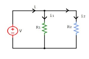
Current divider circuit
image1

Let us take a circuit with a DC voltage source of V volt and two resistors R1 and R2, connected in parallel. The total current in the circuit is i,  current through R1 is i1, and R2 is i2.

What is Current divider theory | Current divider rule definition | Current divider definition ?

Current divider theorem | Current divider principle

The current-divider rule says that the current in any branch of the parallel circuit is equal to the total current in the circuit multiplied by the ratio of the resistance of the opposite branch and the total circuit resistance.

Current divider rule derivation | Formula derivation

Current divider parallel

In the image1, we can see two parallelly connected resistances R1 and R2, are joined with a DC voltage V and currents thru them are i1 and i2, respectively.

The equivalent resistance of the circuit is

{\\displaystyle I_{X}={\\frac {R_{T}}{R_{X}+R_{T}}}I_{T}\\ }
{\\displaystyle {\\frac {1}{R_{T}}}={\\frac {1}{R_{1}}}+{\\frac {1}{R_{2}}}+\\ldots +{\\frac {1}{R_{n}}}}
I_{X}={\\frac {Y_{X}}{Y_{Total}}}I_{T}
I_{X}={\\frac {Y_{X}}{Y_{Total}}}I_{T}={\\frac {\\frac {1}{R_{X}}}{{\\frac {1}{R_{X}}}+{\\frac {1}{R_{1}}}+{\\frac {1}{R_{2}}}+{\\frac {1}{R_{3}}}}}I_{T}

I_{R}={\\frac {\\frac {1}{j\\omega C}}{R+{\\frac {1}{j\\omega C}}}}I_{T}=11 ={\\frac {1}{1+j\\omega CR}}I_{T}\\ ,

What is Voltage and current divider formula ?

Current divider rule formula

According to the currentdivider rule,

Current in through any resistor = Total current of the network x resistance of other resistor/equivalent resistance of the circuit.

Voltage divider rule

According to the voltage divider rule,

The voltage drop across any resistor = Total current of the network x resistance of that resistor

Current divider equation | Derive current divider equation
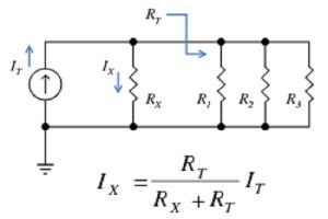
For the above circuit, we can see that resistances R1, R2, R3, and RX are connected in parallel. A voltage source is added to this combination, and current IT flows through the circuit. The equivalent resistance of R1, R2, and R3 is denoted as RT, and If the current across resistor RX is IX, we can say that,

i_{L}={\\frac {R_{out}}{R_{out}+R_{L}}}A_{i}i_{i}\\ .

What is Current divider rule for 2 resistors in parallelly connected ?

Parallel circuit current divider | Current divider formula for parallel circuit

Two resistors R1 and R2, are connected in parallel with a DC source V. If the currents i1 and i2 flow through them and the total current is I then,

{\\displaystyle I_{X}={\\frac {R_{T}}{R_{X}+R_{T}}}I_{T}\\ }
{\\displaystyle {\\frac {1}{R_{T}}}={\\frac {1}{R_{1}}}+{\\frac {1}{R_{2}}}+\\ldots +{\\frac {1}{R_{n}}}}

What is the Current divider rule for 3 resistors in parallelly ?

Current divider rule for 3 resistors

Three resistors R1, R2, and R3, are connected in parallel with a voltage source V. Total current in the circuit is IT and branch currents are i1, i2, and i3, respectively. Therefore,

{\\displaystyle {\\frac {1}{R_{T}}}={\\frac {1}{R_{1}}}+{\\frac {1}{R_{2}}}+\\ldots +{\\frac {1}{R_{n}}}}
I_{X}={\\frac {Y_{X}}{Y_{Total}}}I_{T}={\\frac {\\frac {1}{R_{X}}}{{\\frac {1}{R_{X}}}+{\\frac {1}{R_{1}}}+{\\frac {1}{R_{2}}}+{\\frac {1}{R_{3}}}}}I_{T}

Current in a voltage divider

As the voltage dividers are series circuits, the current through all the resistors or impedance elements is the same. With the help of the total current, the voltage divider rule is constructed. The voltage drop across any resistor equals the total current multiplied by the resistance of that resistor present in the circuitry.

Current divider applications | Current divider examples

  • The main purpose of using a current division is to reduce complexity while solving for current in any circuit. It divides the current into small components.
  • Current division is used to protect circuits from overheating. As it divides the total current into fractions, small current components generate, and large current flow is avoided. This allows less heat dissipation and saves the circuits from any damage.

High current voltage divider

A voltage divider that can deliver a high amount of current is difficult to be built with a traditional resistor network. A switching regulator or a buck converter type design can come in handy in this case. For the buck converter approach, its voltage reference can be replaced with a divider derived from the incoming supply.

Series voltage divider with parallel load current

If a load resistance is connected with the voltage divider in parallel, the overall equivalent resistance decreases. Therefore the current in the circuit increases, but the voltage at the divider output drops.

AC current divider

AC circuits function the same as DC. Just the impedances must be written with their phasor representations using the complex quantity j.

Current divider impedance

If we generalize the resistive network equation for elements other than resistance,

{\\displaystyle {\\begin{aligned}V&=|V|e^{j(\\omega t+\\phi _{V})},\\\\I&=|I|e^{j(\\omega t+\\phi _{I})}.\\end{aligned}}}
{\\displaystyle Z={\\frac {V}{I}}={\\frac {|V|}{|I|}}e^{j(\\phi _{V}-\\phi _{I})}.}
{\\displaystyle {\\begin{aligned}|V|&=|I||Z|,\\\\\\phi _{V}&=\\phi _{I}+\\theta .\\end{aligned}}}

Where IT is the total current, IX is the current through a particular branch, ZT is the equivalent impedance of the circuit, and ZX is the impedance of that branch.

To know about Inductors in Series and Parallel click here

How to use the current divider rule? How to apply the current divider rule? | How to divide current in a parallel circuit?

Current divider method

The current division is calculated in the following steps:

  • First, find the equivalent resistance RT of the other circuit elements, excluding the one for which current needs to be calculated (RX)
  • Compute the fraction of this RT and RT + RX
  • Multiplying this quantity with the total current would fetch the desired branch current IX.

What is the difference between voltage divider and current divider ?

Voltage divider and current divider | Current divider vs voltage divider

Current DividerVoltage Divider
It is constructed through parallel circuits.It is constructed through series circuits.
The values of current through the resistors are measured.The values of voltage drop through the resistors are measured.
The voltages in all the resistors are equal, the currents vary.The currents in all the resistors are equal, the voltages vary.

Low current voltage divider

Voltage divider circuits with low or almost zero current can be used to design switches with an additional transistor.

Voltage divider current limit

There’s no specific limit for current in a voltage divider. However, observed values suggest that currents over 1 amp can be regarded as high for the voltage dividers.

Current divider problems with solutions

Current and voltage divider

Q. Two impedances, Z1 = 2+j5 and Z2 = 5+j2, are connected in a parallel circuit. Total current, I = 10 amp. Using the current division, find out the currents through individual impedances.

We know,

i_{L}={\\frac {R_{out}}{R_{out}+R_{L}}}A_{i}i_{i}\\ .

Therefore, I1 = 10 x (5+j2)/ 2+j5+5+j2 = 5(7-j3)/7 amp

I2 = I – I1 = 10 – 5(7-j3)/7 = 5(7+j3)/7 amp

Current and voltage divider examples | current and voltage divider problems

Q. Three resistors of 6 ohm, 12 ohm, and 18 ohm are connected in series with DC supply voltage 54V, then calculate the voltage drop across all the resistors.

The voltage divider rule says that voltage drop across any resistor in a series circuit = resistance of that resistor x the current.

Now, equivalent resistance of the circuit = 6 + 12 + 18 = 36 ohm

So, net current in the circuit = 54/36 = 1.5 A

Therefore, voltage drop across 6 ohm resistor = 1.5 x 6 = 9 Volt

voltage drop across 12 ohm resistor = 1.5 x 12 = 18 Volt

voltage drop across 18 ohm resistor = 1.5 x 18 = 27 Volt

Current divider rule example problems | Current divider sample problems

Q. 4 resistors with resistances 5 ohm, 10 ohm, 15 ohm, and 20 ohm are connected in parallel with a voltage source. The total current in the circuit is 5A, then compute the current thru the 10Ω resistor.

The equivalent resistance of the circuit = 5 x 10 x 15 x 20 / (50 + 75 + 100 + 150 + 200 + 300) = 17.14 Ohm

Therefore, current through the 10 ohm resistor = 5 x 17.14/10 = 8.57 A

Q. Two resistors of 10 ohm and 20 ohm are connected in parallel with a 200 V DC supply, then compute current thru the 20Ω resistor.

Net resistance in the circuit = 10 x 20/ 30 = 20/3 ohm

Total current in the circuit = 200/(20/3) = 30 A

So the current through 20 ohm resistor = (20/3)/20 x 30 = 10 A

Q. For the network with n resistances shown below, R1 = R2 = R3 = ………= Rn = R. Find the current passing through Rn.

current divider problem

Equivalent resistance of the circuit,

{\\frac {1}{Z_{\\text{eq}}}}={\\frac {1}{Z_{1}}}+{\\frac {1}{Z_{2}}}+\\cdots +{\\frac {1}{Z_{n}}}

We know the total current in the circuit is I

Therefore, current through Rn = (R/n)/R x I = I/n

Frequently Asked Questions | Short Notes | FAQs

Q. How can we calculate the current division?

Current division occurs in a parallel circuit. The supply current gets divided into branches connected in parallel. The voltage across all the branch resistors is equal to voltage supplied. With the help of Ohm’s law and Kirchhoff’s current law, the current division is calculated. The divided current in one branch is the multiplication of the total current and the ratio of the other branch’s resistance with the sum of all the resistance.

Q. In which condition is the current divider rule applicable?

The currentdivider rule is applicable for any circuit where resistance or other impedance parameters are connected in parallel.

Q. What is the advantage of applying the current-divider rule in a parallel circuitry ?

The basic reason for using the current-divider rule in parallel circuits is to make problem-solving easier. In a parallel circuit, the current gets divided into branches, So calculating current thru the branches becomes less time-consuming if the total current is known.

Q. Does the current division rule disobey Ohm’s law?

The Current-divider rule is based on Ohm’s law itself. The fundamental concept of Ohm’s law is used to calculate the divided currents.

Q. State the difference between a voltage divider and a current divider?

The main difference between a voltage divider and a current-divider is the operating circuit. The Voltage divider rule is applied in series circuits where as the current-divider rule is utilized in parallel circuit.

Q. When can we apply the voltage divider and the current divider rule?

In a series circuit, the voltage divider rule is used to calculate the voltage drop across the resistors. In a parallel circuit, the current-divider rule is used to calculate the branch currents.

Q. What are the voltage dividers?

The voltage dividers are linear circuits where the output voltage is obtained from the fraction of input voltage. The most common example of voltage is a potentiometer.

Q. How to use a rheostat so that it works as a potential divider and current limiter?

A rheostat can be used as a large variable resistor. It has three terminals, two at the ends and one movable contact. By adding voltage sources at the ending terminals, the voltage across the other terminal is obtained. This way the rheostat works as a potential divider, and the terminals work as current limiters.

Q. What are the advantages of a voltage divider?

A voltage divider helps in getting the voltage drop across components from the large supply voltage.

Q. How can we calculate the value of current passing through the resistor R1 in the circuit?

The current through resistor R1 is the total current multiplied by the other resistance divided by the sum of all resistance in the circuit.

Q.Why cannot we use the voltage divider method to get a constant current?

The supply voltage keeps fluctuating in a circuit. So we cannot get a constant current.

Q. Three parallel branches with resistances are connected across a DC voltage. What would be the ratio of the branch currents I1, I2, and I3 if the branch resistance ratio is  R1: R2 : R3 = 2 : 4 : 6?

Let us assume that R1 = 2x ohm, R2 = 4x ohm and R3 = 6x ohm

Equivalent resistance of the circuit = 2x x 4x x 6x/ 8×2 + 24×2 + 12×2 = 12x/11 ohm

Therefore, I1 = I x 12x/11/(2x) = 6I/11 A

I2 = I x 12x/11/(4x) = 3I/11 A

I3 = I x 12x/11/(6x) = 2I/11 A

So I1 : I2 : I3 = 6:3:2

Q. Can we apply the voltage divider rule in an ac circuit?

Voltage divider rule is equally applicable for AC circuit calculations, but only if phasor representation is used involving the imaginary quantity ‘j’.

Q. How to obtain zero output voltage using a potential divider?

Zero output voltage can be achieved by keeping a potentiometer in series with a resistance. When this combination is subjected to supply voltage, an end terminal and the middle terminal of the potentiometer fetch output. When the slider terminal is at one end, the voltage is zero.

Q. In a series RC circuitry, the voltage across the capacitor and resistor are 60V & 80V, then What will be total voltage in the circuitry?

By simply applying voltage divider rule, the total voltage is the summation of the voltages across the resistors and the capacitors, So Total voltage = VR+VC=60+80=140V.

Q. Current flow is divided between the different branches in a __.

The answer would be parallel circuitry.

Q. Does a voltage divider affect current?

A voltage divider is nothing but a parallel circuit,will not affect the total current of the circuit. However, the branch current values differ according to the branch impedance.

Q. Is current divided in a parallel circuit?

By the rule of current division, we can say that the parallel circuits divide current flowing through them.
For more article click here.

What is Mutual Inductance? | All important concepts and 10+ formulas you need to know

mutual inductance1 300x200 1

Concept of mutual inductance | Mutual inductance definition

In two adjacent conductor coils, the variation in current in one coil will cause induced emf in the other coil, This phenomenon is called mutual induction. Mutual induction is not a single coil’s property as both/multiple the inductor/inductors are impacted by this property at same time. The primary coil is the coil in which variation of current takes place, and the 2nd coil in which emf is induced named secondary.

Unit of mutual inductance | SI unit of mutual inductance

The unit of mutual inductance is same as inductance, i.e. So SI unit of mutual inductance is Henry(H).

Dimension of mutual inductance

Dimension of mutual inductance = dimension of magnetic flux/dimension of current = [MLT-2I-2]

Mutual inductance equation

Mutual induction is the principle that current running through a conductor will generate a magnetic field, and a changing magnetic field will induce a current in another conductor.
From Faraday’s law and Lenz’s law, we can write,

E = -(dφ/dt)

E ∝ dφ/dt

We already know, ? ∝ i [ as B=μ0ni and ?=nBA]

Therefore, E ∝ di/dt; E =-Mdi/dt [M is proportionality constant]

This M is called the mutual inductance.

M = -E/(di/dt)= emf induced in the secondary coil/rate of change of current in the primary coil

We can also write by comparing that,

-Mdi/dt = dφ/dt

Integrating both sides, we get, ? = Mi

Define Mutual Inductance of 1 Henry

This is the measurement in one coil having 1 m2 area, produced 1 V by the variation of the inducing current of 1 Amp/sec in other coil in the existence of 1 T magnetic field.

Derive an expression for mutual inductance

Mutual inductance circuit analysis | Mutual inductance equivalent circuit

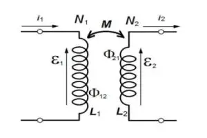
Let us consider, two inductor coils with self-inductance, L1 and L2, are kept in close contact with each other. Current i1 flows through the first one, and i2 flows through the second one. When i1 changes with time, the magnetic field also varies and leads to a change in magnetic flux linked to the 2nd coil, the EMF is induced in the 2nd coil due to the change in current in the 1st coil and can be expressed as,

E21 = -N2(dφ21/dt)

Therefore, N2φ21 ∝ i1

Or, N2φ21 = M21i1

Or, M21= N2φ21/i1

This proportionality constant M21 is called the mutual inductance

Similarly we can write, N1φ12 = M12}i2 or M12 = N1φ12 /i2

M12 is called another mutual inductance

Mutual inductance of a coil
Define mutual inductance between a pair of coils

The mutual inductance of a pair of coils is the ratio of magnetic flux linked with one coil and current passing through another coil.

gif 2 3

Where, μ0=permeability of free space
N1, N2 are turns of the coil.
A is the cross-sectional area of the coil.
L is the length of the coil.

Mutual inductance formula | Mutual inductance of two solenoids

Mutual inductance between two coils,

M = μ0N1N2A/L if there’s no core in between two coils

M = μ0\\μrN1N2A/L if the soft iron core is placed between the coils

How to find the mutual inductance of two long co-axial solenoid ?

Derivation of mutual inductance of two long coaxial solenoids

Let us assume that two solenoids S1 and S2, are placed in close contact with each other. Due to the phenomenon of mutual induction, the current passing through 1st coil will induce EMF in the another coil. Now, we connect S1 with a battery through a switch and S2 with a galvanometer. The galvanometer detects the presence of current and its direction.

Due to the flow of current in S1, magnetic flux is generated in S2, and a change in magnetic flux causes the current in S2. Due to this current, the galvanometer needle shows deflection. Therefore we can say current i of S1 is proportional to ? in S2.

? ∝ i

? = Mi

Here M is called mutual inductance.

Now, in the case of coaxial solenoids, one coil is placed inside another so that they share the same axis. Suppose S1 and S2 have turns N1, N2, and areas A1, A2 respectively.

Mutual inductance formula derivation

For inner coil S1:

When current i1 flows through S1, magnetic field, B10N1i1

Magnetic flux linked with S2, φ21 = B1A1 = μ0N1i1A1

This is the flux for a single turn. [Though the area of S2 is A2, the flux will only generate in the area A1]

Therefore for N2 turns φ21 = μ0N1i1A1 x N2/L …..(1), where L is the length of the solenoids

We know,
? = Mi
?21 = M21i1…….(2)

Equating (1) and (2), we get,

M21i1 = μ0N1i1A1N2/L
M21 = μ0N1A1N2/L

For outer coil S2:

When current i2 flows through S2, magnetic field, B2 = μ0N1i2

Magnetic flux linked with S1 for N1 turns, φ12 = N1/L x B2A1 = μ0N1N2i2A1/L ….(3)

Similar to the inner coil we can write,
?12 = M12i2……(4)

Equating (1) and (2), we get,

M12i2= μ0N1N2i2A1/L
M12 = μ0N1N2A1/L

From the above two findings, we can say that M12=M21 = M. This is the mutual inductance of the system.

Mutual inductance of a coil inside a solenoid | Mutual inductance between two loops

A coil with N2 bindings is placed inside a long thin solenoid that contains N1 number of bindings. Let us assume that the bindings of the coil and the solenoid are A2 and A1, respectively, and the length of the solenoid is L.

It is known that the magnetic field inside a solenoid due to current i1 is,

B = μ0N1i1/L

Magnetic flux that passes through the coil due to the solenoid,

?21 = BA2cos? [? is the angle between the magnetic field vector B and area vector A2]

φ21 = μ0N1i1/L x A2 cosθ

Mutual inductance, M = φ21N2/i1= μ0N1N2 A2 cosθ/L

Mutual inductance in parallel

In this circuit 2-inductors having self-inductance L1 and L2, are adjoined in parallel, Let us assume the total current is i, the sum of i1( current through L1) and i2(current through L2) Mutual inductance between considered as M.

i= i1 + i2

di/dt = di1/dt+ di2/dt

Effective flux through L1, ?1 = L1i1 + Mi2

Effective flux through L2, ?2 = L2i2 + Mi1

Induced EMF in L1,

gif 11

Induced EMF in L2,

gif 12

We know in case of parallel connection, E1 = E2

-L1(di1/dt) – Mdi2/dt = E … (1)
-L1(di2/dt) – Mdi1/dt = E … (2)

Solving the two equations, we get,

di1/dt = E(M-L2)/L1L2 – M2

di2/dt = E(M-L)/L1L2 – M2

gif 10

We know, E = -Leff (di/dt)

Or, Leff =-E/(di/dt) = L1L2 – M2/L1-L2-2M

To know more about the Inductors in series and parallel click here

Calculating mutual inductance between circular coils | Mutual inductance of two circular loops

Let us take two circular coils of radii r1 and r2 sharing the same axis. The number of turns in the coils are N1 and N2.
The total magnetic field in the primary coil due to current i,

B = μ0N1i2r1

Magnetic flux produced in the secondary coil because of B,

gif 9 1

We know mutual inductance,

gif 8 3

Factors affecting mutual inductance | Mutual inductance M is dependent on what factors

  • Material of the core- Air core or Solid core
  • No of Turn (N) of the coils
  • Length (L) of the coil.
  • Cross-sectional area(A).
  • Distance(d) between the coils.
  • Alignment/Orientation of the coil.

Mutual inductance coupling | Coupling coefficient k

The fraction of the magnetic flux generated in one coil that is linked with another coil is known as the coefficient of coupling. It is denoted by k.
Coefficient of mutual inductance,

gif 7 2
  • If coils are not coupled, k = 0
  • If coils are loosely coupled, k<½ If coils are tightly coupled, k>½
  • If coils are perfectly coupled, k = 1

The formula for self-inductance and mutual inductance

Self-inductance L = N?/i = number of turns in the coil x magnetic flux linked with the coil/current flowing through the coil
Mutual inductance M = ?/i = magnetic flux linked with one coil/current passing through another coil

Mutual inductance between two parallel wires

Let us think that two parallel cylindrical wires carrying equal current, each of l length and radius a. Their centers are d distance apart.
The mutual inductance between them is determined with the help of Neumann’s formula.

M = 2l[ln(2d/a) -1 + d/l] (Approximately)

Where, l>>d

What is the difference between self and mutual inductance ?

Self-inductanceMutual inductance
Self-inductance is the property of an individual coil.Mutual inductance is shared by both the coils
It is the ratio of the total magnetic flux produced in the coil and the current.It is the ratio of the total magnetic flux produced in one coil and the current passing through another coil.
If the own current increases, the induced current opposes that.If the own current of one coil increases, the induced current in the other coil opposes that.

What are the application of self induction and mutual induction ?

Applications of self-inductance

The principle of self-induction is used in the following devices-

  • Choke coils.
  • Sensors.
  • Relays
  • DC to AC converter.
  • Ac filter.
  • Oscillator circuit.

Applications of mutual inductance

The principle of mutual induction is used in the following devices-

  • Transformers.
  • Metal detector.
  • Generators.
  • Radio receiver.
  • Pacemaker.
  • Electric motors.

Mutual inductance circuits | Mutual inductance circuit example

T-circuit:

Three inductors are connected like a T-shape as shown in the figure. The circuit is analyzed with the two-port network concept.

Π-circuit:

Contrarily, two coupled inductors can be created using a π equivalent circuit with optional ideal transformers at each port. The circuit can look complicated initially, but it can further be generalized into circuits that have more than two coupled inductors.

What is the Difference between mutual induction and mutual inductance ?

Mutual induction vs Mutual inductance

Mutual inductance is the property shared by two inductive coils in which varying current in one coil induces EMF in the another one, If mutual induction is the cause, mutual inductance can be said to be its effect.

Mutual inductance dot convention

The relative polarity of the mutually coupled inductors decides whether the induced EMF is additive or subtractive. This relative polarity is expressed with dot convention. It is denoted by a dot sign at the ends of the coil. At any instance, if the current enters a coil through the dotted end, mutually induced EMF on the other coil will have a positive polarity at the dotted end of that coil.

Energy stored in mutually coupled inductors

Let us assume that two mutually coupled inductors have self-inductance values L1 and L2. Currents i1 and i2 travel in them. Initially, the current in both the coils is zero. So the energy is also zero. The value of i1 rises from 0 to I1, while i2 is zero. So the power in inductor one,

gif 6 2

So, the energy stored,

gif 5 3

Now, if we keep i1 = I1 and increase i2 from zero to I2, the mutually induced EMF in inductor one is M12 di2/dt, while the mutually induced EMF in inductor two is zero since i1 does not change.
So, the power of inductor two due to mutual induction,

gif 4 3

Energy stored,

gif 3 2

The total energy stored in the inductors when both i1 and i2 have reached constant values is,

w = w1 + w2 = 1/2L1I12 + 1/2L2I22 – MI1I2

If we reverse the current increments, that is, increase i2 from zero to I2 first and later increase i1 from zero to I1, the total energy stored in the inductors is,

w = w1 + w2 = 1/2L1I12 + 1/2L2I22 – MI1I2

Since, M12 = M21, we can conclude that the total energy of mutually coupled inductors is,

w = w1 + w2 = 1/2L1I12 + 12L2I22 + MI1I2

This formula is correct only when both the currents enter dotted terminals. If one current enters the dotted terminal and the other leave, the energy stored will be,

w = w1 + w2 = 1/2L1I12 + 1/2L2I22 – MI1I2

Mutual inductance devices

Mutual inductance transformer model

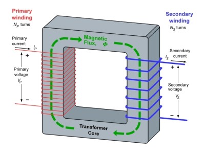
An AC voltage can be increased or reduced according to the requirements of any electrical circuit by using a static device. It is called a transformer. It is a four-terminal device that consists of two or more mutually coupled coils.
Transformers follow the principle of mutual induction. They transfer electric energy from one circuit to another when the circuits are not electrically connected.

Linear transformer:

If the coils in the transformer are wound on magnetically linear material, then it is called a linear transformer. Magnetically linear materials have constant permeability.

In a linear transformer, magnetic flux is proportional to the current passing through the windings. The coil that is directly joined to a voltage source is known as the primary coil and the coil adjoined to load impedance is entitled as secondary. If R1 is connected in the circuit with the voltage source and R2 is connected in the circuit with the load.

Applying Kirchhoff’s voltage law in two meshes, we can write,

V = (R1 + jΩL1)I1 – jΩMI2……(1)

-jΩ MI1 + (R2 + jΩL2 + ZL)I2 = 0.…..(2)

Input impedance in the primary coil,

Zin = V/I1 = R1+ jΩL1 + Ω2M2/R2+jΩL2 + ZL

The first term (R1+jωL1) is called the primary impedance and the other second term is called the reflected impedance ZR.

ZR = Ω2M2/R2+jΩ L2 + ZL

Ideal transformer

A transformer that doesn’t have any type of loss is called an ideal transformer.

Characteristics:

  • An ideal transformer has zero primary and secondary winding resistance.
  • Permeability of the core is considered as infinite.
  • No leakage flux is there in an ideal case.
  • Hysteresis does not take place.
  • The value of eddy current loss is zero.
  • The ideal transformer is said to be 100% efficient.

Mutual inductance of transformer formula-

There’s zero power loss in an ideal transformer. So, the input power = output power

W1i1cosφ = W2i2cosφ or W1i1 = W2i2

Therefore, i1/i2 = W2/W1

Since voltage is directly proportional to the no. of turns in the coil.,
we can write,

V2/V1 = W2/W1= N2/N1 = i1/i2

If V2>V1, then the transformer is called a step-up transformer.
If V2<V1, then the transformer is called a step-down transformer.

Applications of transformer:

  • A transformer can electrically isolate two circuits
  • The most important application of a transformer is to step up ( increase) or step down (decrease) the voltage. It can raise or lower the value of current and voltage so that if any of the quantities increase or decrease, power remains the same.
  • It can also increase or decrease the impedance, capacitance, or inductance values in a circuit. In other words, the transformer can perform impedance matching.
  • Transformer will prevent carrying direct current from one circuit to other.
  • It is used in mobile chargers to avoid damages caused by high voltage.
  • It is used to generate a neutral in three-phase power supply.

Heaviside Mutual Inductance Bridge | Mutual Inductance measurement bridge

We use mutual inductance in various circuits to determine the values of self-inductance, frequency, capacitance, etc. Heaviside bridge is a component where we can measure mutual inductance with the help of a known self-inductance. A modified version of this bridge can be used in performing the reverse application i.e. measuring self-inductance with the help of known mutual inductance.

Operation

Let us take a combination of elements in the form of the bridge circuit shown in the figure. The coil S1 with mutual inductance M is not the part of the bridge but it is mutually coupled with the coil S2 in the bridge which has self-inductance L1. Current passing through S1 produces flux that is linked with S2. As per the dot convention, we can say, current i passes through S1 and further gets divided into i1 and i2. The current i1 passes through S2.

Under balanced condition,
i3=i1; i4=i2 ; i=i1+i2

As no current passes through the galvanometer, the potential of B is equal to the potential of D.

Therefore we can say, E1=E2

Or, (i1+i2)jΩM + i1(R1+jΩ L1) = i2(R2+jΩ L2)

i1R1+jΩ (L1i1+ M(i1+i2))= i2R2 + jΩ L2i2 …..(1)

i1[R1+jΩ (L1+M) = i2[R2+jΩ (L2-M)] ……(2)

Similarly, E3=E4

i3R3=i4R4

Or, i1R3=i2R4…….(3)

Dividing (1) by (3) we get,

R1+jΩ (L1+M)/R3 = R2 + jΩ (L2-M)/R4

Taking the real parts of both sides, we can write,

R1/R3=R2/R4

Taking the imaginary parts of both sides, we can write,

L1+M/R3=L2-M/R4

So, M=R3L2-R4L1/R3+R4

We can conclude from the above equation that the value of L1 must be known. Now if R3=R4,

R1=R2 and M = L2-L1/2

Or, L2= L1+2M

This way we can find out the value of unknown inductance L2

The bridge that measures the unknown mutual inductance in terms of two known self-inductance L1 and L2, is called the mutual inductance measurement bridge or Campbell bridge.

The field-armature mutual inductance of the synchronous motor

In an AC rotating synchronous motor, steady-state speed is proportional to the frequency of the current passing through its armature. Therefore, a magnetic field is produced. The current rotates at the same speed as that of the rotating synchronous speed of the field current on the rotor. Due to this phenomenon, a mutual induction develops between the armature and the field wingdings. It is known as field-armature mutual inductance.

Notch Filter: 19 Facts You Should Know

image 51 300x100 1

In this article, we will study detail about notch-filters.

Notch Filter Definition

Before discussing in detail about notch-filter, let us find out the definition of it. A notch-filter can be defined as a band stop that has a very narrow frequency bandwidth. Great depth, high-quality factor, and sharpness in band-reject characterize a notch-filter. There are several kinds of notch-filters which we will discuss later.

Checkout these two articles for more details –

Notch Filter Equation

Some of the important equations of notch-filter are given below.

  • The HF cut-off of the LPF: fL = 1 / ( 2 * RLP * CLP * π)
  • The LF cut-off of the HPF: fH = 1 / ( 2 * RHP * CHP * π)
  • The quality factor of the notch filter:  Q = fr / Band Width

How does a notch filter work ?

Working of notch filter

A notch-filter has the same working principle as of band-reject filter. It allows all other frequency components of the signal and blocks the specified narrow bandwidth. For a passive design, the resistive, capacitive and inductive reactance play the part of controlling the frequency.

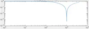
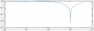
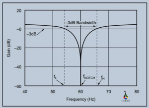
Notch filter graph | Notch filter phase response

The following is the notch-filter graph.

Notch Filter

Notch Filter Q

Q of a notch-filter is a very important parameter. Q or Quality Factor of a Notch-filter is given by the following equation: Centre Frequency/Bandwidth. Q is the measurement of the selectivity of the filter.

The center frequency is the Notch Frequency, and it is the center frequency of the passband.

Notch filter applications | Use of notch filter

There are several applications of different kinds of notch-filters. Let us discuss some of them.

  • Communication Systems: Notch-Filters is one of the important pieces of equipment for a communication system. There is a high probability that the message signals get interfered with by harmonic noises in long-term communication. Notch-filters eliminate the noise.
  • Audio Engineering: One of the basic components of audio engineering is a notch-filter. Eliminating noise, spikes are some of the tasks performed by a notch-filter.
  • Medical Engineering: Notch-filters have been used in Medical Engineering. Reading of EEG is impossible without a notch-filter.
  • Digital Signal Processing: Notch-filters have applications in Digital Signal Processing. A notch-filter is important when there is a need for mixing up signal or condition of elimination of certain frequency component.
  • Digital Image Processing: Notch-filters help to eliminate noises from digital images.
  • Optical Applications: Notch-filters have applications in optical applications. Blocking off a certain wavelength of light is done by specific optical notch-filters.

Notch filter EEG

EEG or Electroencephalogram is a very important process in medical sciences. Several filters are used to display the output data produced by the machine. Without the filters, it is quite impossible to read the values.

There are three kinds of filters used in an EEG reading. They are – high pass filter, low pass filter, and notch-filter. High pass filter filters out high-frequency components, whereas low pass filters do the same for common frequency components. The notch-filters filter out a certain given range of frequency.

Especially the supplied frequency of the AC interferes with the EEG readings. Notch-filter removes such interference. For North America, the supply frequency is 60 Hz, so a 60 Hz notch-filter is used. In India and other countries where the supply frequency is 50 Hz, a 50 Hz notch-filter is used.

Optimum notch filter in image processing

There is certain kind of periodic noises in digital images. The noises are repetitive and unwanted. They create certain patterns and affect the picture badly. One of the solutions to the problem is an optimum notch-filter.

At first, the noise frequency is determined, then the notch-filter produces the repetitive noise, and the output with lesser noise is produced.

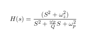
Notch filter transfer function

The following expression gives the transfer function of a notch-filter –

Notch Filter

Here, wz refers to the Zero-Circular Frequency, whereas wp refers to the pole-circular frequency. Finally, q means the Quality Factor of the notch-filter.

How to use a notch filter ?

When there is a need to reject a certain narrow band of frequency, a notch-filter is used. A notch-filter is placed after any source from which the signal needs to be eliminated. In most cases, the filter is set as the very last component of any circuit.

Difference between notch filter and band stop filter

A notch-filter is one type of bandstop filter. The only difference between a band stop filter and a notch-filter is that a notch-filter has a narrower bandwidth than a normal bandstop filter.

Bandpass vs Notch filter

There are some differences between the bandpass filter and the notch-filter. Let us elaborate on them.

Points of DiscussionBandpass FilterNotch-Filter
PrincipleAllowing certain bandRejecting certain band
BandwidthComparatively wider band is passed.A comparatively narrower band is rejected.

Anti notch filter

Notch-filters reject the very narrow bandwidth of signals and allow other components of that signal. The same but opposite task is performed by bandpass filters. The bandpass filters allow passing a certain band of frequency and block different parts of the movement.

Notch filter characteristics

Some of the attributes of a notch-filter –

  • Narrow bandwidth
  • High Q value
  • Great depth

Notch filter high q

Twin T notch-filters can provide a very good amount of depth, almost infinite. If an LM102 voltage follower is added to the network, the Q of the circuit gets a skyrocketing growth from 0.3 to 50. That is how a high Q is achieved.

Gain of notch filter

The gain of a notch-filter can be calculated using the following equation.

Notch Filter

Notch filter coefficients

Notch-filter coefficients are referred to as the coefficients of the transfer functions.

Notch Filter

Here, wz refers to the Zero-Circular Frequency, whereas wp refers to the pole-circular frequency. Finally, q means the Quality Factor of the notch-filter.

Transfer function of notch filter in s domain

The following expression gives the transfer function of a notch-filter –

Notch Filter

Different types of Notch-Filters

Active notch filter

An active notch-filter is a combinational circuit of two separate circuits. For example, connecting a low pass filter and a high pass filter in a parallel connection and adding an op-amp for amplifying purposes will work as an active notch-filter.

Inverse notch filter

Inverse notch-filter is a special type of Notch-filter that has an infinite impulse response. Inverse notch-filters are very useful in medical image processing where there is a need to eliminate narrowband signals. Inverse notch-filters do the job efficiently.

Cavity notch filter

Notch-filters are a special type of Cavity filter. Cavity filters allow a certain narrow band of frequency. So, we can say that the working is the same as notch-filters. That is why often cavity filters and-notch-filters are termed cavity notch-filters.

Adjustable notch filter | Adaptive notch filter

Adjustable notch-filters are also tunable notch-filters. One can adjust the frequency as per the need. Some of the Adjustable notch-filters are very important in audio engineering.

Adjustable q notch filter

Adjustable q notch-filters can change the Q value of the notch-filter. Therefore, the Q is a very important parameter of the filter.

The adjustable Q value is needed for the audio engineering department.

Bandpass notch filter | Notch band pass filter

Notch-filters are a special type of bandpass filter. Bandpass filters allow a certain band of frequency to pass. In bandpass filters, theoretically, any range of rounds can be given by the required design. But, in bandpass filters, the band’s scope is typically narrower than the usual ones.

Notch filter VST

VST is a filter envelope plugin. An envelope provides several edges to a filter. VST notch-filters offer many advantages like mixing up audios very finely, etc.

FM Notch filter

FM notch-filters or Frequency Modulation notch-filters are some of the important instruments for Software-Defined Radios. Even these filters made the Software-defined Radios popular. It also helps in radio communications.

Tunable fm notch filter

Tunable FM notch-filters are special kind of notch-filters which can adjust the center frequency as per the need of the applications. No need to say again that the FM filters need the tunable filters because several frequency bands need to be blocked from a signal in FM.

RF Notch filter

RF or Radio-Frequency Notch-filters are used to reject only one frequency from a given band of frequency. Generally, RF notch-filters have a Q. Basic RF filters are designed from low-pass filters to achieve high efficiency. However, converting them into a notch-filter is a tough process and needs a high level of caution and efficiency. 

Tunable notch filter RF

Just like other tunable notch-filters, the tunable rf notch filter can adjust the frequency band as per the need.

60 Hz Notch filter EEG

EEG or Electro-Encephalograph Machines has an inbuilt 60 Hz notch-filter. The high pass filters and low pass filters are fixed at their highest and lowest calibrations.

What is a 60 Hz filter? Click Here!

60hz Notch filter IC

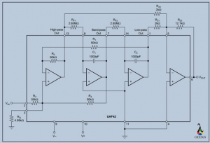
There is a readymade filter IC available to minimize the circuit. It includes one low pass and one high pass filter, and one op-amp for summing up the outputs of both the filters. The most popular 60hz notch-filter IC from Texas Instruments is UAF42.

Circuit of 60 Hz filter… Click Here!

50 Hz notch filter

A 50 Hz notch-filter can reject a 50 Hz signal by keeping the power of the movement almost intact. A 50 Hz notch-filter is needed when the 50 Hz band is necessary to be accurately rejected.

50 Hz notch filter circuit

A 50 hz circuit can be designed using the same frequency of a 60 hz notch-filter as given previously. Some typical values for creating a 50 Hz filter are given below. C= 47 nano-farad, Resistance R1, R2 = 10 kilo-ohm, R3, R4 = 68 kilo-ohm.

switched capacitor notch filter

A switched capacitor notch-filter is another advanced topology. This topology provides high precision, high Q value. This topology has several applications.

HF notch filter

HF Notch-Filter stands for High-Frequency Notch-Filters. Notch-filters of 50-60 Hz cannot give a good depth value or a high Q. High-frequency notch-filters (which rejects or allows a high-frequency component) are more realistic, provides a desired bandwidth and depth.

1khz notch filter

A one kilo-hertz notch-filter has a basic principle, the same as the previously discussed 50 hz or 60 hz filters. The only difference is that a one khz notch-filter is more realistic and can be designed for real-time applications. The 50-60 Hz filters are capable of giving 40 to 50 dB depth. But as an engineer, one must focus on the depth and the Q value. So, the one khz filter comes into action.

Notch filter in frequency domain

Notch-filters deal with frequency. The main principle of a notch-filter is to block a certain narrow band of frequency. So we can say the notch-filter works in the frequency domain only.

2 meter notch filter

A 2 meter notch-filter is a solution to a very general communication problem called – intermodulation. But the filter suffers a high loss during operation.

Audio notch filter

A notch-filter is an important instrument for audio engineering. Generally, some unwanted frequency components get mixed up in the original audio. To remove or eliminate such frequency, an audio notch-filter is used.

Notch filter equalizer

A notch-filter can be used as an equalizer in audio engineering. It can help to find out several unwanted spikes or noise, and also, it can remove those noise and spikes. That is how it helps to make the audio clear.

Periodic noise reduction using a notch filter

There is certain kind of periodic noises in digital images. The noises are repetitive and unwanted. They create certain patterns and affect the picture badly. One of the solutions to the problem is an optimum notch-filter.

At first, the noise frequency is determined, then the notch-filter produces the repetitive noise, and the output with lesser noise is produced.

Acoustic notch filter

As mentioned earlier, Notch-filters are important for audio engineering. After the audio is being recorded, different audio or acoustic audio is needed to mix up. There is a probability that any spike gets introduced in the mix-up. An acoustic notch-filter can remove such noise and spikes.

Variable notch filter

Variable notch-filters are essential for audio engineering. These kinds of notch-filters can change the intended frequency in a certain range.

In audio engineering, several unintended frequencies may present; to remove them, we need notch-filters. Instead of using one filter to omit a single frequency is not a great solution. Variable notch-filters serve our purpose here.

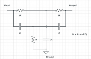
T Notch filter

T notch filter is a basic notch-filter with a ‘T’ network of RCR components. It is a special design technique.

Double T Notch filter | Double notch filter

Double T notch-filter or Twin T filter is an updated version of the T network. As the name suggests, here, two T networks are connected to form a notch-filter. One network consists of RCR components. Another is of CRC components.

Crossover notch filter

Crossover notch-filters can be described as series of notch-filters connected. These filters are designed so, to eliminate the driver resonance from the filter networks.

Series notch filter

Series notch-filters are used for the elimination of the driver resonance. Series notch-filters are designed using Capacitor, Resistance, and an Inductor. All the components are connected in a series connection, and the driver is connected in parallel with them.

Parallel notch filter

Parallel notch-filters are specially designed to eliminate significant unwanted peaks from the driver’s response. This filter is similar because all the basic elements are connected in parallel, unlike the series notch-filter.

High Q notch filter

High Q notch-filters are popular for providing great depth in rejection. Generally, Twin T notch-filters are used to get a high q value and get more depth—the Q value changes from normal 0.3 to 50 for a Twin T filter.

Sallen key notch filter

Sallen Key is a topology for designing higher-order filter circuits. Using this topology, notch-filters can also be created. The topology is also termed as Voltage Controlled Voltage Source. R.P. Sallen and E.P. Key first started it in the year 1955. Therefore, the topology is named after them.

Butterworth notch filter

Butterworth filters provide the flattest possible frequency response. So now, if a notch-filter is designed to provide a flat response, then the notch-filter will be called a Butterworth notch-filter.

AM Notch filter

AM Notch-Filter or Amplitude Modulation Notch-filter is designed to help the measurement of emission of a broadcasting station using a spectrum analyzer. AM Notch-filter is very useful for AM radio communication stations when there are nearby other towers. This is because it can allow only AM band EAS reception while the other strong fields are present.

Dynamic notch filter

The dynamic filter is a set of algorithms. First, the algorithm finds the noise frequencies. Then, active notch-filters are used to eliminate such spikes of noise.

Microstrip notch filter

As we can see, there are several filters available in the market for different uses. But Microstrip notch-filters are especially useful for wireless communication systems.

Analog notch filter

A notch-filter can be classified into the main domain; one is Analog another – Digital. We have previously discussed Digital Notch-filter, like – IIR, FIR, etc. Analog notch-filters are RLC notch-filters, RC notch-filters, T notch-filters, Twin T notch-filters, etc.

RC Notch filter

RC notch-filters are analog notch-filters that are designed with resistors and capacitors. In this kind of filter, manually, we can supply values of r and c.

IC Notch filter

LC notch-filters are analog notch-filters that are designed with an inductor and capacitor. In this kind of filter, manually, we can supply values of L and c.

Arduino Notch filter

Several digital filters can be designed using Arduino. Writing appropriate codes will help an engineer to realize even Notch-Filter digitally. The digital filter codes are available on GitHub. Try to modify them to make a notch-filter.

Coax stub Notch filter

Coax stub notch-filter is a type of notch-filter build within coaxial cables to remove noise and attenuation. ‘T’ coaxial connector will be very useful for designing such a filter. The addition of a second stub will be very helpful to improve the situation. Radio, Television centers use this filter.

FM broadcast notch filter

Almost in every major city, there is a high possibility that one can receive the radio frequency from the FM radio stations. The FM broadcast notch-filter will provide a 30db attenuation for the FM signals in the range of 88 to 108 MHz.

GPS Notch filter

GPS notch-filters help to catch the satellite signals. However, the basic rule is that the GPS module will receive a comparatively weaker signal from the satellite. This is because the nearby located towers may interfere with the incoming signal.

The GPS notch-filter will help here to attenuate the signal by – 30 dB. In addition, it will allow the GPS module to receive a fairer band from the satellite.

Bainter Notch filter

Bainter notch-filter is nothing but a basic notch-filter. A notch-filter consisting of one low pass filter, one high pass filter, and one adder to get the output frequency response can be termed a Bainter Notch-filter.

Wideband notch filter

If a band-reject filter has a wideband frequency as the operational band, then the filter is technically a wideband filter. If the band-reject filter has a narrow band of frequency, the filter is known as the Notch-filter. So, a Notch-filter cannot be a wideband notch-filter. It is technically impossible.

Eagle notch filter

A QAM notch-filter is based upon the phase cancellation concept. Eagle Comtronics Inc designs this narrow network. That is why QAM notch-filters are popular as Eagle Notch-Filter.

Crystal notch filter

Notch-Filters can be designed using crystals also. A crystal has a very high-Quality factor. A crystal notch-filter is useful for creating a notch-filter that has a very narrow band.

Peak notch filter

It is a digital notch-filter. The filter can resist each channel of an input signal for a certain center frequency and a bandwidth of 3 dB.

Narrow notch filter | Narrow band Notch filter

Notch-filters reject a very sharp band of frequency, saying a very narrow band of frequency. That is why notch-filters are often termed narrow notch-filters.

TV channel Notch filter | TV Notch filter | Cable Notch filter

The TV notch-filters help to solve the modulation problem that could occur in the transmission line. The tv notch-filter can make room for the modulated channel once it is installed in the queue. The filter also prevents reverse broadcasting to the coaxial cable. The increasing bandwidth now increased the demand for cable television notch-filters.

MNE Notch filter

MNE is popular software which provides us platform to build several electronics instrument. For example, we can design certain notch-filters in the MNE platform by writing some specific code.

Opposite of Notch filter

Notch-filters reject the very narrow bandwidth of signals and allow other components of that signal. The same but opposite task is performed by bandpass filters. The bandpass filters allow passing a certain band of frequency and block different parts of the signal.

Automatic Notch filter

An automatic notch-filter is something that can change the center frequency as well as the Q value as per the need. Several mechanical systems use these kinds of filters.

Gaussian Notch filter

A gaussian notch-filter is a digital filter. This filter is used to remove noise from various digital images. The specialty of the filter made it popular and is used in multiple applications as well as in various investigating agencies.

Notch filter parameters

There are some parameters to measure the accuracy of the notch-filter. One of the important among them is the Q factor or Q (Details given above). Another is the depth of the output. Finally, the bandwidth is also one of the parameters.

Notch filter impulse response

The following image shows a notch-filter impulse response.

Notch Filter

Second order Notch filter transfer function

The following expression shows the second order notch-filter’s transfer function.

Notch Filter

Master Slave Flip Flop with all important Circuit and Timing Diagrams and 10+ FAQ

image 33 300x145 1

Content: Master Slave Flip Flop

Master Slave Flip Flop Definition

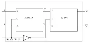
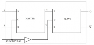
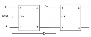
Master-slave is a combination of two flip-flops connected in series, where one acts as a master and another act as a slave. Each flip-flop is connected to a clock pulse complementary to each other, i.e., if the clock pulse is in high state, the master flip-flop is in enable state, and the slave flip-flop is in disable state, and if clock pulse is low state, the master flip-flop is in disable state, and the slave flip flop is enable state.

Master Slave Flip Flop is also Referred to as.

Pulse-triggered flip flop because the flip-flop  can enabled or disabled by a CLK pulse during this mode of operation.

Master Slave Flip Flop Diagram

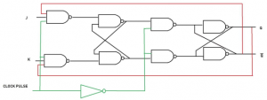
Assume that in the initial state Y=0 and Q=0, the next input is S=1 and R=0; during that transition, the master flip-flop is set and Y=1, there is no change in slave flip-flop as slave flip-flop is disabled by the inverted clock pulse, when the clock pulse of master changes to ‘0’, then the information of Y passes through slave and Q=1, in this clock pulse the slave flip-flop is active and master flip-flop gates deactivated.

Master slave flip flop
Fig. Master slave flip flop logic diagram.

Master Slave Flip Flop Circuit | Master Slave Flip Flop Circuit Diagram

image 34
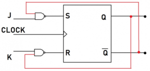
Fig. Clocked master slave JK flip flop

Master Slave Flip Flop Timing Diagram

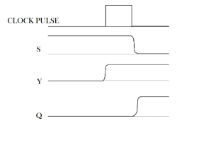
The changes in input and output with respect to time can be defined in the timing diagram.

The behaviour of a master-slave flip flop can be determined through a timing diagram. For example, in the given figure below, we can see a signal of the clock pulse, S is the input signal to the master flip flop, Y is the O/P signal of the master flip flop, and Q is the output signal of slave flip flop.

image 35
Fig. Time relationship of master slave flip-flop.

Master Slave Flip Flop Truth Table

The truth table is a description of all possible output with all possible input combinations. In the master slave flip flop, there are two flip flops connected with inverted clock pulse to each other, so in the master slave truth table in addition to flip flop states, there must be an additional column for clock pulse so that the relationship between the input and output with the clock pulse can be determined.  

Application of Master Slave Flip Flop

Mater slave configuration is mainly used to eliminate the race around the condition and get rid of unstable oscillation in the flip flop.

Advantages of Master Slave Flip Flop

Master slave can be operated on level triggered or edge triggered clock pulse; it can be used in various ways.

  • A sequential circuit with an edge-controlled flip flop is straightforward to design rather than a level-triggered flip flop.
  • By using the Master slave configuration, we also can eliminate the race around the condition.

Master Slave JK Flip Flop

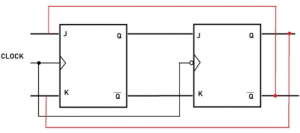
Master slave JK flip-flop could have been designed utilizing 2 JK flip-flops, in that each flip-flop is connected to CLK pulse complementary to each other, and the first flip flop is the master flip-flop which works when the CLK pulse is high state. And at that time the slave flip flop is in the hold state and if the CLK pulse is low state, then the slave flip-flop works, and the master flip-flop stays in the hold state.

The JK flip-flop characteristic is more or less similar to the SR flip-flop, but in SR flip flop, there is one uncertain output state when the S=1 and R =1, but in JK flip flop, when the J=1 and K=1, the flip flop toggles, that means the output state changes from its previous state.

JK Master Slave Flip Flop Circuit Diagram

image 36
Fig. JK master salve block circuit diagram.

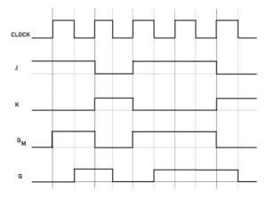
JK Flip Flop Master Slave Timing Diagram

image 37
Fig. Timing Diagram for JK Master slave flip flop

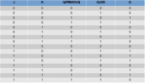
Master Slave JK Flip Flop truth table

image 38

Master Slave JK Flip Flop Working

A master slave flip flop can be edge-triggered or level-triggered, which means it can either change its output state when there is a transition from one state to another, i.e., edge-triggered. The output of the flip flop changes at high or low input, i.e., level triggered. Master-slave JK flip flop can be used in both triggered ways; in edge-triggered, it can be +ve edge-triggered or -ve edge triggered.

In edge-triggered, the master flip flop is derived from the +ve edge of the clock pulse. At that time, the slave flip flop is in the hold state, i.e., the output of the master is according to its input. When the negative clock pulse arrived, the slave flip flop is activated. The o/p of the master flip-flop propagates through the slave flip-flop; at that time the master flip-flop is in the hold state.

Working:

  • When J = 0, K = 0, there will be no change in the output with or without clock pulse.
  • When J = 1, K = 0, and clock pulse is on positive edge, the output of master flip flop Q is set as high, and when the negative edge of the clock arrives, the output of master flip flop passes through the slave flip flop and produce output.
  • When J = 0, K = 1, and clock pulse is one positive edge, the output of master flip flop Q is set as low and Q’ is set as high, when the negative clock edge arrives the Q’ output of the master flip flop feed into the slave flip flop, and that causes to set the output of the slave Q as low.
  • When J = K = 1, then at the positive edge of the clock pulse, the master flip flop toggles (means the change of the previous state into its opposite state), and at the negative edge of the clock pulse, the slave flip flop toggles.

Master Slave JK Flip Flop Verilog Code

module jk_master_slave(q, qbar, clk, j, k);
output q, qbar;
input j, k, clk;
wire qm, qmbar, clkbar;
not(clkbar, clk);
jkff master(qm, qmbar, clk, j, k);
jkff slave(q, qbar, clkbar, qm, qmbar);
endmodule
module jkff(q, qbar, clk, j, k);
input j, k, clk;
output q, qbar;
always @(posedge clk)
 case({j,k})
  2'b00:
    begin
     q<=q;
     qbar<=qbar;
    end
  2'b01:
    begin
     q<=0;
     qbar<=1;
    end
  2'b10:
    begin
     q<=1;
     qbar<= 0;
    end
  2'b11:
    begin
     q<=~q;
     qbar<=~qbar;
    end
 endcase
endmodule

VHDL_code

library IEEE;
use IEEE.STD_LOGIC_1164.ALL;
entity jkff is
port(p, c, j, k, clk: in STD_LOGIC;
q,qbqr: out STD_LOGIC);
end jkff;
architecture Behavioral of jkff is
signal input: std_logic_vector(1 downto 0);
begin
input <= j & k;
process(clk, j, k, p, c)
variable temp: std_logic:=’0’;
begin
if(c=’1’ and p=’1’) then
if rising_edge(clk) then case input is
when “10” => temp:= ‘1’;
when “01”=> temp:= ‘0’;
when “11”=> temp:= not temp;
when other => null;
end case;
end if;
else
temp=’0’;
end if;
q<= temp;
qbar<= not temp;
end process;
end behavioral

Advantages of Master Slave JK Flip Flop

JK flip flop master slave over come the limitation of SR flip flop, in SR flip flop when S = R = 1 condition arrives the output become uncertain, but in JK master slave when J = K = 1, then the output toggles, the output of this state keep changing with the clock pulse.

Application of Master Slave JK Flip Flop

JK flip flop master slave overcome the limitation of SR flip flop, in SR flip flop when S = R = 1 condition arrives the output becomes uncertain. Still, in the JK master slave, when J = K = 1, then the output toggles, the output of this state keeps changing with the clock pulse.

Master Slave D Flip Flop

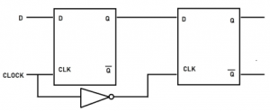
In this master slave also, two D flip flop connected to each other in series with clock pulse invited to each other. The basic mechanism of this master slave is also similar to other master slave flip-flops. D master slave flip flop can be level triggered, or edge triggered.

Master Slave D Flip Flop Circuit Diagram

image 39

Fig. Block representation of master slave D flip flop circuit.

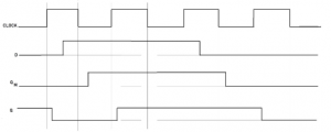
Master Slave D Flip Flop Timing Diagram

In the diagram, one signal of the clock pulse, one is D, the i/p to the master flip flop, Qm is the o/p of the master flip flop, and Q is the o/p of the slave flip flop.

image 40

Fig. Master Slave D flip flop timing diagram

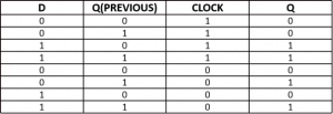
Master Slave D Flip Flop Truth Table

image 41

Master Slave D Flip Flop using NAND gates

The master slave D flip flop can be designed with NAND gates; in this circuit, there are two D flip flops, one is acting as a master flip flop, and the other is acting as a slave flip flop with an inverted clock pulse to each other. Here for inverter also NAND gats are used.

image 42

Fig. Circuit diagram of Master Slave D flip flop designed with NAND gates.

Master Slave edge triggered D Flip Flop

When the state of a flip-flop changes during the transition of a clock, the pulse is known as an edge-triggered flip-flop and these can be +ve edge-triggered, or -ve edge-triggered. The +ve Edge triggered flip flop means the state of it changed during the transition of the CLK pulse from ‘0’ to ‘1’ state. The ve edge triggered flip flop implies the state of flip flop changes during the transition of the clock pulse from ‘1’ to ‘0’ state.

image 43

Fig.  D- type positive edge master slave flip flop.

The positive edge triggered d master slave flip flop is designed with three basic flip- flop as shown in the above figure; S and R are maintained at logic ‘1’ for the output to remain steady. When S=0 and R=1, the output Q=1, where for S=1 and R=0 the output Q=0. When the clock pulse changes from 0 to 1, the value of D transferred to Q,  change in D when the clock pulse is maintained at ‘1’ the value of Q does not get affected by it, and a transition from 1 to 0 also does not cause changes the output Q, nor when the clock pulse is ‘0’.

But in the practical circuit, there is a delay, so for proper output, we need to consider setup time and hold time for proper operation. A definite time before the clock pulse arrives, the requirement of the value of D should be assigned that time is called the setup time. Hold time is the time for which input should behold after the clock pulse arrives.

RS Master Slave Flip Flop

Master slave is a configuration to prevent the unstable behavior of a flip flop; Here in RS master slave flip flop, two RS flip flop are connected to form master slave configuration, here flip flop is connected to a clock pulse inverted to each other; when the positive half of the clock pulse arrives the master flip flop is activated, and during negative clock pulse the slave flip flop is activated. Each flip flop works at different time interval.

In master salve configuration of RS flip flop, an unsalable oscillation cannot take place, because at a time master flip flop is in hold state or the slave flip flop is in hold state. For proper working of mater salve flip flop, we must consider hold time and setup time which can vary from one circuit to another; it depends on the design of the circuit.

image 44
Fig. Block Representation of RS master slave flip flop

Master Slave SR Flip Flop Timing Diagram

Here, there is one clock signal, S is the input signal to the master flip flop, R is also an I/p signal to the master flip-flop, Qm is the O/P of the master flip-flop, Q if the O/P signal of the slave flip-flop.

image 45
Fig, Timing Diagram of master slave SR flip flop.

Master Slave T Flip Flop

image 46
Fig. Block diagram of Master Slave T flip flop

FAQ/Short Notes

What do you mean by flip flop? | What is Flip Flop with example?

The flip flop is a fundamental element in the sequential logic circuit, a bi-stable element,  as it has two stable states: ‘ 0,’ and the other is ‘1’. It can store only 1-bit at a time and a flip-flop circuit capable to maintain its state indefinitely or until when power is delivered to the circuit. The O/P state of the flip flop can be changed with input and clock pulse to the flip flop. When a latch circuit is added with some basic gates and clock pulse, it is a flip flop. Example of flip flop is D flip flop, SR flip flop, JK flip flop, etc.

What is S and R flip flop?

In a SR flip-flop, the S stands for the set and R stands for reset;because of this, it is also named as the Set Reset flip-flop. It can be designed with two AND gates and a clock pulse to an SR-latch. When the clock pulse is ‘0’, any input value through S or R cannot change the output value Q, and when the clock pulse is ‘1’, the value of output Q depends on the input values of S and R.

image 47
Fig. Diagram of SR flip-flop

What are the types of flip flop?

There are four types of a flip flop:

  1. SR FFs.
  2. JK FFs.
  3. D FFs.
  4. T FFs.

What is a JK flip flop?

JK flip flop characteristic is more or less similar to the SR flip flop, but in SR flip flop, there is one uncertain output state when the S=1 and R =1, but in JK flip flop when the J=1 and K=1, the flip flop toggles, that means the output state changes from its previous state.

JK flip flop can be designed by adding AND gates to the input of S and R in SR flip flop, the input J and output Q’ is applied to the AND gate attached with S and input K, and the output Q is applied to the And gate connected to R.

image 48
Fig. JK flip flop is designed with SR flip flop.

How does JK flip flop works?

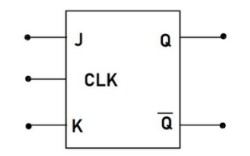
When the clock is not provided, or the clock is low, the input change cannot affect the output. So, for manipulation of output with the input clock, the pulse must be high.

image 49
Fig. Block diagram of a JK flip flop.

Working of JK flip flop when the clock pulse is high:

  • When J = 0 and K = 0, there will be no change in the output.
  • When J = 0 and K = 1, then the value of output will get reset.
  • When J = 1 and K = 0, then the value of output will get set.
  • When J = 1 and K = 1, the output value gets toggled (means to switch to the opposite state). In this state, the output will continuously change with the clock pulse.

Why JK flip flop is used?

JK flip flop is more versatile than D- flip flop or SR flip flop; they can operate more function than any other flip flop, they are widely used to store binary data. JK flip flop also overcome the uncertain states of SR flip flop.

How does JK flip flop toggle?

When the input to the flip flop J = K = 1 with clock pulse high, that’s when the JK flip flop toggles.

Why D flip flop is called delay?

The next output state of the D flip flop follows the input D, when the clock pulse is applied, in this way the input data is transfer to the output with delay, that’s why it is called a delay flip flop.

What are the applications of flip flop?

The flip flop is generally used as a

  • The memory elements. 
  • In the shift-registers. 
  • The digital counters.
  • The freq. Divider circuits.
  • The bounce elimination switch, etc.

What are the characteristics of flip flop?

It is a synchronous sequential circuit; it changes its output state only when the clock pulse is present. It is the basic memory element for any sequential circuit, it can store one bit at a time. It is a bistable device.

What is the difference between D and T flip flop?

  • D flip flop can not take similar input as D and D’ is its two input, so the input is always complementary to each other. On the other hand, Both the input in T is the only T so both inputs to the T flip flop will always be the same.
  • D flip flop is a delay flip flop, in this flip flop, the output follows the input with the arrival of the clock pulse, whereas the T flip flop is called a Toggle flip flop, where the output changes to the opposite state with every arrival of the clock pulse when the input is 1.

Where are D flip flop used?

It is commonly used as a delay device or to store 1-bit data information.

Notch Filter Circuit: 35 Important Factors Related To It

image 29 300x89 1

In this article we will discuss about different kinds of notch filter circuit. Let’s see the points of discussion for the article.

Points of Discussion

  1. notch filter definition
  2. what does a notch filter do?
  3. notch filter vs low pass
  4. Notch Filter Block Diagram
  5. notch filter circuit || notch filter circuit diagram || active notch filter circuit
  6. notch filter schematic
  7. notch filter cutoff frequency
  8. notch filter bandwidth || bandwidth of notch filter
  9. notch filter bode plot || notch filter frequency response || notch filter response
  10. lc notch filter design
  11. notch filter ic
  12. 60hz notch filter
  13. 60hz notch filter circuit
  14. rf notch filter circuit
  15. audio notch filter design || audio notch filter circuit
  16. audio notch filter schematic
  17. digital notch filter transfer function
  18. low pass notch filter
  19. high pass notch filter
  20. 2.4 ghz notch filter
  21. quarter wave stub notch filter
  22. optical notch filter
  23. 532 notch filter || 532 nm notch filter
  24. 785 nm notch filter
  25. multi notch filter
  26. holographic notch filter
  27. laser notch filter
  28. notch filter raman spectroscopy
  29. fliege notch filter
  30. fpv notch filter
  31. dc notch filter
  32. helical notch filter
  33. tinnitus notch filter
  34. bridged t notch filter
  35. microwave notch filter

notch filter definition

Before discussing about circuits of notch filter, let us find out the definition of notch filter. A notch filter can be defined as a band stop that has a very narrow frequency bandwidth. Great depth, high-quality factor, and sharpness in band-reject characterize a notch filter. There are several kinds of notch filters which we will discuss letter.

what does a notch filter do?

A notch filter does the work of a band-stop filter in a more specified way. As the band reject filter rejects the given band of frequency from the main signal, the notch filter does the same. But, for a notch filter, the band of frequency is much narrower. Notch filter basically attenuates the given band of frequency which is the exact opposite of a band pass filter where a certain band of frequency is allowed while the other bands are rejected.

notch filter vs low pass

Let us discuss some differences between a notch filter and a low pass filter. It will also help to understand the difference between a band pass filter and band reject filter.

Points of DiscussionLow Pass FilterNotch Filter
1. Passing Frequency BandOnly Low-frequency components are allowed to pass. (Certain limits are set previously)All frequency except a narrow band gets passed.
2. Blocking frequencyHigh-frequency filters are blocked.The narrow, specified frequency band is blocked.
3. BandwidthComparatively wider band is passed.A comparatively narrower band is rejected.
Notch Filter Circuit Table – 1

Notch Filter Block Diagram

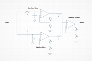
Notch filter is a combinational circuit of Low pass Filter and High Pass Filter. The block diagram given below depicts the basic concept of a notch filter.

image 29
Notch Filter Circuit: Block Diagram

rlc notch filter

In general, most of the Notch filters are designed using three basic components. They are – Resistance, Capacitance, and Inductor. Therefore, if any notch filter is developed using these elements, that notch filter can be termed RLC Notch Filter. Almost all RLC filters are passive filters as they does not contain any active element like operational amplifier. For that, these filters also deprived of the amplification process.

notch filter circuit || notch filter circuit diagram || active notch filter circuit

Here is a circuit diagram of notch filter. It is a circuit of active notch filter, as we can see operational amplifiers are used. We can also see, the circuit is combination of both low pass filter as well as high pass filter. The summing amplifier sumps up the output from the low pass filter and high pass filter. It also provides amplification of the signal.

notch filter circuit
Notch Filter Circuit

notch filter schematic

The Notch filter circuit is a very simple and easy-to-understand circuit. The only complex part of the circuit is the op-amp. Check out my article on operational amplifiers to get the schematic diagram of an operational amplifier.

notch filter cutoff frequency

The cutoff frequency is the parameter using which one can analyze a filter. In general, the cutoff frequency of a notch filter refers to the frequency of the narrowband which needs to be blocked through the filter. It is an important parameter for designing the notch filter circuit.

  • The HF cut-off of the LPF: fL = 1 / ( 2 * RLP * CLP * π)
  • The LF cut-off of the HPF: fH = 1 / ( 2 * RHP * CHP * π)

notch filter bandwidth || bandwidth of notch filter

Notch filters have very narrow bandwidth. Also, it is the reason why a notch filter is made out of a band-reject filter. The sharpness is depended on the Q of the notch. Normal band reject filter has a wider bandwidth than the notch filter. It is another important parameter for designing the filter. Bandwidth is also associated with the performance parameter of the filter.

notch filter bode plot || notch filter frequency response || notch filter response

Bode plot of a filter refers to the graphical representation of frequency response. Let us find out the response of a notch filter. The following plot describes the depth, bandwidth of a signal after it passes through a notch filter. It is an important parameter to determine the accuracy of the notch filter.

image 25
Notch Filter Circuit 2: Frequency Response

lc notch filter design

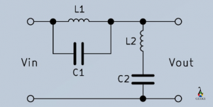
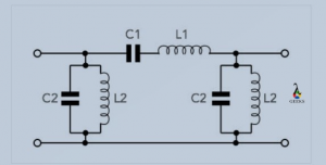
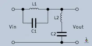
A notch filter can be designed using inductor and capacitor also. It will be a passive filter as it has no active component like operational amplifiers. The design procedure is given in the notch filter design article. Check it out here. The notch filter circuit diagram is given below.

image 26
Notch Filter Circuit 3: LC Notch

notch filter ic

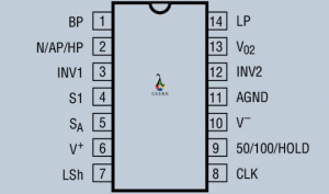
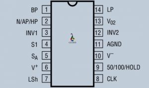
Notch filter can be designed inside an Integrated Circuit. There are plenty of ICs available in market which functions like notch filter. One of the commonly used IC is the LTC1059. The pin diagram of the IC is given below.

image 27
Notch Filter Circuit 5: LTC 1059 Pin Diagram

60hz notch filter

As the name suggest, a 60 Hz filter attenuates 60 Hz of frequency. The filtering is done using a notch filter because notch filter provides a sharp depth. 60 Hz filters are so popular because it is the supply frequency of USA. Other countries like India has a frequency supply frequency of 50 Hz. That is why 50 Hz filters are also used to remove supply interference. These types of filters are mainly used in ECG, EEG machines (the details are given in the Notch filter Design article).

60hz notch filter circuit

The 60 Hz notch filter is designed using several op amp. Some of them are to realise the Low pass filter, some of them to realise the high pass filter. The IC UAF42 is used to get rid of such complicated circuit. The value of registers and capacitors are given within the circuit diagram. While designing the circuit, make sure you use the exact value of the resistor and capacitors to get a more accurate result. The 60 hz notch filter circuit is given below.

image 30
60 Hz Notch Filter Circuit

rf notch filter circuit

Radio Frequency notch filter has several applications. The circuit is designed using the inductors and capacitors only. At first, one capacitor and one inductor is placed in parallel. Then a set of capacitor and inductor are placed in series with the previous connection. Then another pair of inductor and capacitor (Values are equal to the first used set) are placed in parallel, in series with the second connection. The circuit is given below.

image 31
RF Notch Filter Circuit

audio notch filter design || audio notch filter circuit

Audio notch filter is a very important filter for audio engineering. Notch filters removes the spike and noises to make the audio better. The circuit diagram of a basic audio notch filter is given below. As we can see, the circuit can be designed using passive elements like – resistors and capacitors. The generalised values of them are also given. As the circuit is passive one, there is no amplification part.

image 32
Audio Notch Filter Circuit

audio notch filter schematic

A schematic diagram is something which is represented by basic elements. The audio notch filter has quite a simple design. As we can see in the circuit, it is already drawn with basic elements. You can still try to simplify the circuit.

digital notch filter transfer function

Transfer function is an important expression in control system engineering. It is referred as the mathematical expression which provides output for every set of input. The following expression gives the transfer function of a digital notch filter –

image 50

Different Types of Notch Filters

low pass notch filter

Notch filters are made up of both high pass and low pass filters. Low pass filters allow the lower frequency band of a signal. Notch filters allow a narrow band of frequency resisting other bands.  If the wz< wp, it is common to pass notch type. (Check the transfer function derivation in the other article to understand).

high pass notch filter

As mentioned earlier, Notch filters come with both the high pass and low pass filters. High pass filters allow the higher frequency band of a signal. A notch filter can allow any narrow band of the signal. So, if a notch filter is designed to pass a narrow band of the high-frequency component, then the filter can be said a high pass notch filter.  If the wz> wp, it is a high pass notch type. (Check the transfer function derivation in the other article to understand).

2.4 ghz notch filter

We have seen notch filters are useful in minimizing interferences. Radar systems use a wide range of signals. These signals are transmitted towards various places from the air. Now, there are several electronics equipment and appliances which work on different frequency levels. Therefore, there is a high probability that the signals might get interfered among each other.

A 2.4 GHz is designed to omit or eliminate such kinds of interferences and provide a smoother service.

quarter wave stub notch filter

Quarter wave stub has several applications. If a quarter wave stub is left with an open end, it can be used as a notch filter, attenuating a certain frequency band. That is how the purpose of a notch filter is served. It is one of the important types of filter for research and development purpose. It has several other applications also.

optical notch filter

There are also notch filters in Optics. Unlike an electronics notch filter, the optical notch filter blocks a specific wavelength of light and allows the other wavelength to pass smoothly. As notch filters work for narrow bandwidth, the optical notch filter can have 10 nm. Optical notch has a lot of variety. The applications depends on the need of the notch filter.

532 notch filter || 532 nm notch filter

532 notch filter represents 532 nm optical notch filter. This optical filter is named so because it can block the light component of 532 nm wavelength and allow all other wavelengths. These filters have applications in scientific researches.

785 nm notch filter

785 notch filter represents 785 nm optical notch filter. This optical filter is named so because it can block the light component of 785 nm wavelength and allow all other wavelengths. Just like 53nm optical notch, it has also applications in scientific researches and applications.

multi notch filter

Multi-notch filters are a kind of variable notch filter for optics. In optics, notch filters are also used where we can eliminate a certain wavelength. A multi-notch filter can block multiple wavelengths at once.

holographic notch filter

A holographic Notch Filter or HNF is one type of optical notch filter. These kinds of filters can give a high laser attenuation for narrower bandwidth. HNF has application in Laser Spectroscopy.

laser notch filter

As one can guess, Laser Notch Filter is a kind of Optical Notch Filter. Laser filters are used to block a certain wavelength of laser light. There is various kind of laser notch filter available in the market. They are useful for laser-based Raman devices and Biomedical systems.

notch filter raman spectroscopy

Let us understand what Raman spectroscopy is. It is a chemical analysis that can provide us very detailed info on chemical structure. Raman spectroscopy comes into the picture when there is an interaction of light with any chemical particle.

To realize Raman Spectroscopy, a light source is needed as well as a spectrometer. Now, light is emitted from the start and caught in the spectrometer. To remove the unwanted lights, the optical notch filter is used.

2nd order notch filter || second order notch filter

In general, a filter is called a second-order filter when it has one more RC network along with a first-order network. A notch filter is a 2nd order filter as it comes with a low pass filter and a cascaded connection of a high pass filter.  2nd order notch filter has cut-off frequencies. Sallen Key feature topology is used to make higher

fliege notch filter

Fliege notch filter is another notch filter topology. There are several advantages of this topology over the twin T notch filter. First, the center frequency can be tuned using only the four precision components, i.e., two resistors and two capacitors.

One of the great features of the topology is that if there any slight mismatch, the center frequency gets affected, but the depth of the filter remains the same.

The Q of the filter can also be adjusted using two independent resistors.

fpv notch filter

These refer to 433/1.3 GHz notch filters which can filter out interference in the 1.2- 1.3 GHz frequency band if the filter is used in the 433 MHZ RC transmitter.

dc notch filter

There are several dc notches filters available. One of the most widely used applications is the GPS notch filter. The notch filter helps to eliminate interference and receive the satellite signal.

helical notch filter

Let us know what a helical filter is. A helical filter is made of a series of cavities that are further magnetically coupled. These filters provide a high Q and great performance.

Now a Helical filter can be turned into a notch filter if one of the taps of the helix is being attached to the transmission line. The depth of the notch filter will be around thirty to forty dB.

tinnitus notch filter

At first, let us know what Tinnitus is. Tinnitus is a hearing problem. If one experiences a buzzing or ringing noise in one or both o his/her ear(s), then the syndrome is called Tinnitus.

As a remedy to it, conventional hearing aids are suggested by doctors. But it is recently observed that if a notch filter is added for the tinnitus frequency, the mechanism will improve and help the recovery process.

bridged t notch filter

A bridged t notch filter is quite a different type of filter. The filter provides a shallow depth and also comes with a frequency band that is wider than the available notch filter. It is used where a need for equalization is there. It is also not considered an active filter.

microwave notch filter

A dual-drive Mach-Zander modulator achieves a microwave Notch Filter. It is efficient, and the frequency can be adjusted. Therefore, it has a higher value of the frequency band.

Notch Filter Design: 37 Interesting Facts To Know

Notch 1 300x151 1

In this article, we will discuss different techniques of notch filter design. Let’s see what are the points of discussions for this article.

Points of Discussion

  1. What is notch filter?
  2. how to build a notch filter
  3. notch filter eq || notch filter equation
  4. notch filter ic
  5. notch filter q factor
  6. notch filter frequency
  7. notch filter example
  8. Notch filter design || rlc notch filter design || how to design a notch filter
  9. tunable notch filter
  10. tunable notch filter design
  11. digital notch filter
  12. digital notch filter design
  13. dsp notch filter
  14. design of notch filter in dsp
  15. fir notch filter
  16. fir notch filter design
  17. iir notch filter || digital iir notch filter
  18. iir notch filter design
  19. active notch filter design || analog notch filter design || notch filter derivation
  20. lc notch filter design
  21. notch filter using op amp || notch filter circuit using op amp
  22. 60hz notch filter
  23. 60 hz notch filter design
  24. rf notch filter design
  25. programmable notch filter
  26. notch filter code
  27. fm broadcast notch filter
  28. audio notch filter
  29. audio notch filter design || audio notch filter circuit || fm notch filter circuit
  30. audio notch filter schematic
  31. biquad notch filter
  32. 532 nm notch filter
  33. harmonic notch filter
  34. notch filter design tool
  35. betaflight notch filter
  36. notch filter transfer function derivation
  37. notch filter for ecg signal

What is notch filter?

A notch filter is generally a modified form of the Band Reject or Band Stop filter. The main objective of these filters is to stop or prohibit a certain range of frequencies from appearing in the output. For example, a Band Stop filter having a narrow stopband is called a notch filter.

Let us take an example. Suppose a Notch filter is designed to stop frequency between 100kHz to 110kHz. So, it will pass every signal below the 100kHz range and give any signal higher than 110kHz but will prevent any signal in between the 100kHz to 110 kHz.

how to build a notch filter

The building of a notch filter is quite easy. There are three main steps in building a notch filter. The steps are – 1. Note down the requirement perfectly, 2. Understand the need and design the notch filter (Designing a notch filter is written below), 3. Check with the expectation. (If perfect, then use, if not re-design the filter).

notch filter eq || notch filter equation

Some of the important equations of notch filter are given below.

  • The HF cut-off of the LPF: fL = 1 / ( 2 * RLP * CLP * π)
  • The LF cut-off of the HPF: fH = 1 / ( 2 * RHP * CHP * π)
  • The quality factor of the notch filter:  Q = fr / Band Width

notch filter ic

There are several Integrated Circuit available in the market which implement a notch filter. There are many advantages of using IC over conventional circuits. One of the most popular normal notch filter IC is LTC1059. The PIN diagram of the IC is given below.

LTC1059 1
PIN diagram of LTC 1059

notch filter q factor

The q factor of a notch filter is the same as the q of a notch. Q or Quality Factor of a Notch filter is given by the following equation: Centre Frequency/Bandwidth. Q is the measurement of the selectivity of the filter. It also gives an idea of sharpness of the depth.

The center frequency is the Notch Frequency, and it is the center frequency of the passband.

notch filter frequency

The frequency of the notch filter is referred to as the frequency of the stopband. This is because the narrow band’s frequency is what the notch filter rejects. Therefore, the frequency is also the identity of the notch filter.  

notch filter example

There are several examples of notch filters. There are numbers of types also. Every types has sub topics as well as many examples. Digital notch filters, analog notch filters, optical notch filters, FM notch filters, audio notch filters, helical notch filters, tunable notch filters, 50hz notch filters, and 60 Hz 2.4 GHz notch filters. Some of the examples are based on their specifications. Like – 532 nm notch filter. It is a optical filter te blocking wavelength is specified with the name.

Notch filter design || rlc notch filter design || how to design a notch filter

Let us design a notch filter from scratch. First, let us create an RLC type filter(notch) to eliminate the band of 45 kHz to 50 kHz. Say, the inductance is L = 30 mH.

So, the given datas are: fL = 45 kHz, fH = 50 kHz, l = 30 mH = 0.03 H

The resonant frequency will be: fr = fH – (BW/2)

The BW is Bandwidth and BW = 50 – 45 = 5kHz.

Or, fr = 50 *103 – ((5 * 103)/2)

Or, fr = 50000 – 2500

Or, fr = 47.5 * 103

So, the Resonant frequency is 47.5 kHz.

Now, we know that resonant frequency can be written as –

fr = 1 / [2 * pi * (LC)1/2]

or, 47.5 * 103 = 1 / (1.088 * C1/2)

or, C = 374.41 pico-Henry

So the Quality factor will be = fr / BW = 47500/5000 = 9.5

Again, Q = wr L / R

Or. R = wrL/Q = 2 * pi * f * L/Q

Or, R = 8.95 kilo-ohm

So for the notch filter, R = 8.95 kilo-ohm, L = 30 mH, C = 374.41 pico-farad.

tunable notch filter

Tunable notch-filters are such narrowband filters where we can manually get the high rejection from a particular frequency and comparatively lower attenuation from other frequency signals. There are several tunable notch-filters available in the market, like – EM-7843. Tunable filters can be of another type. If the Q factor of a notch filter is tuneable that filter can also be termed as tuneable notch filter.

tunable notch filter design

The design of the Tuneable notch filter is not so simple. It requires a lot of calculation and concept. But the creation of a digital tuneable notch filter is somewhat easy. The design should be made such that one can change the centre frequency easily.

digital notch filter

Digital notch filters refer to the FIR Notch-filter and IIR Notch-Filter. FIR and IIR both have their advantages in different conditions and are used as per the requirement. They are termed digital because they are designed digitally.

digital notch filter design

Digital notch filters have two types of design techniques. They are – Infinite Impulse Response Notch Filter (IIR), Finite Impulse Response Notch Filter (FIR). We have discussed both the filter details below.

dsp notch filter

 DSP stands for Digital Signal Processing. The notch filters used in the digital processing of signals are termed DSP notch filters. Therefore, it is fairly understandable that only digital filters are used as DSP notch filters. The FIR, IIR notch filters are an example of these kinds of filters.

design of notch filter in dsp

Digital notch filters have two types of design techniques. They are – Infinite Impulse Response Notch Filter(IIR), Finite Impulse Response Notch Filter. We have discussed both the filter details below.

fir notch filter

FIR filters stand for Finite Impulse Response filter. FIR filters generally come with lots of stability, which made them famous. When the stability of the system is more necessary, then these types of filters are used.

fir notch filter design

There are several methods of designing an FIR notch-filter, like – frequency sampling and computer optimization. Analytical methods, Semi-Analytical methods, second-order IIR filter prototypes are some other processes of preparing the same. Bernstein polynomials are also used in creating the FIR type digital notch filters.

iir notch filter || digital iir notch filter

IIR stands for Infinite Impulse Response. This is also a digital filter like an FIR filter. IIR filters generally come with an efficient approximation for a very low order requirement. These types of filters are required when the linearity of phases is not that much important.

iir notch filter design

IIR notch filters are designed in two major parts. At first, an analog notch filter is designed with the required specifications, and then the analog filter is transformed into a Digital IIR filter using inverse transformation.

active notch filter design || analog notch filter design || notch filter derivation

Let us design a notch-filter from scratch. First, let us create an RLC type filter(notch) to eliminate the band of 55 kHz to 60 kHz. Say, the inductance is L = 30 mH.

So, the given datas are: fL = 55 kHz, fH = 60 kHz, l = 30 mH = 0.03 H

The resonant frequency will be: fr = fH – (BW/2)

The BW is Bandwidth and BW = 60 – 55 = 5kHz.

Or, fr = 60 *103 – ((5 * 103)/2)

Or, fr = 60000 – 2500

Or, fr = 57.5 * 103

So, the Resonant frequency is 57.5 kHz.

Now, we know that resonant frequency can be written as –

fr = 1 / [2 * pi * (LC)1/2]

or, 57.5 * 103 = 1 / (1.088 * C1/2)

or, C = 255 .51 pico-Henry

So the Quality factor will be = fr / BW = 57500/5000 = 11.5

Again, Q = wr L / R

Or. R = wrL/Q = 2 * pi * f * L/Q

Or, R = 7.39 kilo-ohm

So for the notch-filter, R = 7.39 kilo-ohm, L = 30 mH, C = 255.51 pico-farad.

lc notch filter design

As we can interpret from the name of the filter, the LC Notch-filter is designed using only inductors and capacitors. The design method of an LC notch-filter is quite simple. At first, one inductor and once capacitor is kept at parallel connection. Then another combo of inductor and capacitor is kept in series connection. The circuit diagram is as follows.

Notch 1
LC circuit for notch-filter

The output impedance comes as:

image 11

The transfer function is:

image 12

The cut-off frequencies are –

image 13

notch filter using op amp || notch filter circuit using op amp

Notch filters are realized using operational amplifiers. At first, both the high pass and low pass filters are created using operational amplifiers. Then their outputs are summed up using another operational amplifier to get the outcome. The circuit diagram given in the article depicts a notch filter using op-amps.

60hz notch filter

A 60 Hz notch filter can reject a 60 Hz signal by keeping the power of the movement almost intact. A notch filter is used because it will accurately attenuate the frequency band. A 60 Hz notch filter has demand in the USA because the power supply in households has a frequency of 60 HZ.

60 hz notch filter design

As we know, any notch filter is designed with a high pass filter and a low pass filter. An additional op-amp is needed to add up the output of both the filters. Typically, the Q comes as 6 for a 60 Hz filter. The given equation can determine the notch frequency.

image 14

ALP is the low pass filter’s output when the frequency of the filter is the same as the desired output frequency, whereas AHP is the output for the high pass filter. In general, the

image 15

value is one. So, the notch frequency comes as output frequency, which is 60 Hz.

The following expression can also determine the output frequency:

image 16

As we can observe, the output frequency is dependent on the RF. So, changing the value of Rf will change the notch frequency.

rf notch filter design

Designing an RF filter is a very complicated process. It needs a skilled engineer as accuracy is an important parameter for these kind of filters. The design process of an RF notch filter is given below.

  1. Specify the Response: In his stage, all the required parameter value is specified. Parameters like – Response, cut-off point, etc. are needed to be set.
  2. Frequency Normalization: The frequencies are converted to match the standard tables and charts.
  3. Calculation of Ripple: In this stage, the concept of a notch filter is used. To create an RF notch filter, which can reject only one frequency from a certain frequency band, the ripple value should be considered a high priority. The higher the ripple value tolerance limit, the more selective the filter becomes.
  4. Matching the attenuating curves.
  5. Calculation of element values.
  6. Scaling of normalized values.

programmable notch filter

The most popular filter used nowadays is the Programmable filter. Programmable filters are easy to maintain, easy to work with. Programmable notch filters are no exception. We can control the Q value as well as the natural frequency by just changing the clock frequency.

notch filter code

The notch filter code to design a notch filter in MATLAB is given below. Writing any one of them with the right specifications will provide you a notch filter.

image 17
Code for designing a notch-filter in MATLAB simulator.

fm broadcast notch filter

Almost in every major city, there is a high possibility that one can receive the radio frequency from the FM radio stations. The FM broadcast notch filter will provide a 30db attenuation for the FM signals in the range of 88 to 108 MHz.

audio notch filter

A notch filter is an important instrument for audio engineering. Generally, some unwanted frequency components get mixed up in the original audio. To remove or eliminate such frequency, an audio notch filter is used.

audio notch filter design || audio notch filter circuit || fm notch filter circuit

The following circuit is an example of audio and fm notch design. Carefully observe the resistance and capacitor values before starting the design. The formula for centre frequency is also given.

Notch Filter Design
Audio notch-filter design circuit

audio notch filter schematic

The audio notch filter has quite a simple design. The schematic can be drawn easily for the current condition by following the standard procedures.

biquad notch filter

A biquad filter is a digital filter. More specifically, it is an IIR filter that has two poles and two zeros. The ‘Biquad’ is an abbreviation from the term – Bi-quadratic. Notch filters can also be designed using the topology. The transfer function for the filter comes as:

image 22

532 nm notch filter

532 nm notch filter is a variety of optical notch filters. The specification of the filter is 532 nm, that means the optical notch is able to block the light component having wavelength of 532 nanometre. It is one of the most popular optical notch filter. There are other specifications like 785 nm.

harmonic notch filter

A harmonic notch filter is a special type of notch filter, which has applications in several fields. The filter follows the following transfer function.

H(z)=12(1+A(z))

notch filter design tool

There is a different kind of tools available in the market for designing the notch filter digitally. Many types of digital filters can be created using such devices. It would be best if you assigned the frequency value only. One of the favourite tools is produced by Texas Instruments.

betaflight notch filter

Betaflight is a flight control software where multi-rotor crafts are controlled. As a part of the process, notch filters are also designed and tuned in the software.

notch filter transfer function derivation

The following expression gives the transfer function of a notch filter –

image 23

Here, wz refers to the Zero-Circular Frequency, whereas wp refers to the pole-circular frequency. Finally, q means the Quality Factor of the notch filter.

Q is given by – fr / Bandwidth.

If the ωp = ωz, it is a standard notch type.

If the ωp > ωz, it is a high pass notch type.

If the ωz < ωp, it is a low pass notch type.

notch filter for ecg signal

ECG or Electrocardiograph is a very important process of diagnosis in medical sciences. Several filters are used to display the output data produced by the machine. Without the filters, it is quite impossible to read the values.

There are three kinds of filters used in an ECG reading. They are – high pass filter, low pass filter, and notch filter. High pass filter filters out high-frequency components, whereas low pass filters do the same for common frequency components. The notch filters filter out a certain given range of frequency.

Especially the supplied frequency of the AC interferes with the ECG readings. Notch filter removes such interference. For North America, the supply frequency is 60 Hz, so a 60 Hz notch filter is used. In India and other countries where the supply frequency is 50 Hz, a 50 Hz notch filter is used.

Inductors in series and parallel | Concepts you need to know and 10+ important problems

Table of contents : Inductors in Series and Parallel

What are inductors?

Inductors

Inductors are nothing but magnetic energy storage devices. Physically it is a coil of conducting wire, either wrapped around a solid core or without any core. The latter one is called an air-core inductor. 

When current flows through the inductor, it creates a magnetic field. Coiling up a lot of wire increases the strength of the magnetic field. The direction of the magnetic field is determined with the help of the right-hand thumb rule

When current first starts to flow through the coil, the magnetic field starts to expand, then after some time, it stabilizes and stores some amount of magnetic energy. When the field gradually collapses, the magnetic energy gets turned back into electrical energy. Inductors produce magnetic flux, proportional to the current flowing through them.

To know more about inductive reactance click here.

What is self inductance?

Self inductance Definition

Self inductance is the characteristic of a coil by which the coil opposes any sudden change of current in it. 

Self inductance of a coil,

ezgif 3 20a57524e7

Where, N = number of turns in the coil, ? = magnetic flux and i is the current flowing through the coil

Self inductance of a solenoid with n turns, l length and A cross-sectional area,

ezgif 3 b63e4d7938

What is mutual inductance?

Mutual Inductance Definition

In the case of two coils, the change in current in one coil induces EMF in the neighboring coil. This incident is known as mutual induction, and this property of the primary coil is called mutual inductance.

How to calculate inductors in series ?

Adding inductors in series | Two inductors in series

inductors in series
a Inductors in series circuit

In a inductors in series connection, we can see from the diagram that the current in each inductor is equal. So the total voltage drop across the inductors is the sum of every individual inductor’s voltage drop. Suppose L is the total inductance of the circuit. So total voltage drop VTotal will be

VTotal = V1 + V2 

The V1 and V2 is the voltage drop across the the individual inductor respectively.

By Kirchhoff’s rule we can write,

ezgif 3 22293b35a8
ezgif 3 0af02d6054
ezgif 3 c89293ef65

L=L1+L2

( Answer )

The equivalent inductance of inductors in series  | Formula for inductor in series

Similar to the previously found equation for two inductors, if we connect n number of inductors in series with self inductance L1, L2, L3,…..Ln in series, the equivalent inductance for inductors in series circuit will be, 

Leq = L1 + L2 + L3 + ….. + Ln

( Answer )

How to calculate inductors in Parallel?

Inductors in parallel 

inductors in parallel
Inductors in parallel

In a parallel connection, we can conclude from the diagram that the total current flowing through the circuit is the summation of the individual coil’s current. The voltage across each inductor is the same.

If the supply voltage is V then,

ezgif 3 b92668c99f
ezgif 3 7492cdf1c3
ezgif 3 c5e1929b70
ezgif 4 6fb266e30b

The equivalent inductance of inductors in parallel  | Inductor in parallel formula

The equivalent inductance of n inductors with self inductance L1, L2, L3,…..Ln connected in parallel is,

ezgif 4 64fce7d796

Inductors in series with mutual inductance

For the above derivations, we assumed that there is no mutual inductance in between the inductors. Now, if the inductors are connected in such a manner that the magnetic field produced by one affects the inductance of others, the inductors are said to be ‘mutually connected.’

Coupled inductors in series

The magnetic fields of the inductors can be either aiding or opposing each other depending upon the orientation of the coils. Coupling can be classified into two types-

Series Aiding Type of Coupling :

In this type of coupling, the magnetic fields of the inductors are in the same direction. So the currents that flow through the inductors are also in the same direction. For two inductors with self inductances L1 and L2 and mutual inductance M, we can write,

Total induced EMF = Self-Induced EMFs in L1 and L2 + induced EMF in one coil due to change of current in other for mutual inductance

ezgif 4 293e9045d5

Therefore,

The equivalent inductance =  L1+ L2 +2M

Series opposing type of coupling:

In this type of coupling, the magnetic fields of the inductors are in the opposite direction. So the directions of the currents are opposite to each other. For two inductors with self inductances L1 and L2 and mutual inductance M, we can write,

Total induced EMF = Self-Induced EMFs in L1 and L2 + induced EMF in one coil due to change of current in other for mutual inductance

ezgif 4 b84056a0c3

Therefore, equivalent inductance =  L1+ L2 -2M

What will be Impedance of capacitor and inductor in series LC circuit ?

Impedance of capacitor and inductor in series LC circuit:

ktDUZCHA1 JBhrrEtNCrxWtPngO1t942vnUXD4l2lTkDJqUkhTX GoY995lz k cUw1LJZ28SY5M3Dkt7x1 X5HbqBmXDu8xRKwUc9eDh4YUb9aa4kdpVDHLq4vt4tyeyvPOwV 9
a series LC circuit

For the above capacitor and inductors in series circuit, we are going to assume that there is no resistance. We place a fully charged capacitor along with an inductor in the circuit. Initially, the switch is open. Suppose the capacitor plates have charge Q0 and -Q0

At t=0, the switch is closed. The capacitor begins to discharge , and the current starts increasing in the coils of the inductor with inductance L. Now, if we apply Kirchhoff’s law, we get,

ezgif 4 99bfbed87b

(voltage drop across the inductor is E)

ezgif 4 181835e6d7
ezgif 4 88455e87ce

A solution to this second order differential equation is,

ezgif 4 3182539922

where Q0 and ? are constants depending on the initial conditions

If we put the value of Q in (1), we get,

ezgif 4 1dde0a98ca
ezgif 4 1479d0cf14
ezgif 4 f0fef862bc

Therefore,

ezgif 4 de6194291c
ezgif 4 1c7693b2bb
ezgif 4 c4da4d9f96

Energy stored in LC series circuit

For the above capacitor and inductors in series circuit

Total energy in LC circuit= energy stored in the electric field + energy stored in the magnetic field

ezgif 4 d4af26e9d9
ezgif 4 a765c9726b
ezgif 4 0d144bbd10

[since ⍵=1/LC ]

ezgif 4 499f7253c4

Impedance of capacitor and inductor in series | Impedance in LC circuit

For the above capacitor and inductors in series circuit

Total impedance of LC circuit XLC=XL-XC if XL>XC

                                                      =XC-XL if XL<XC

Inductors in series and parallel problems

An inductor and a capacitor are connected with a 120 V, 60 Hz AC source. For the following LC circuit, find total impedance and the current flowing through the circuit.

6N56pkILfDbJYU1tptpy55IvGOD7zTyOsy2jaqjENhUwdVI6tN7pPS
LC circuit

Given: 

L= 300 mH    C = 50 µF    V = 120 V   f = 50 Hz

We know, XL= 2πfL and  XC= 1/2πfC  

Putting the given value of L and C we get,

XL = 113 ohm

XC= 53 ohm

Therefore, total impedance, Z = XL – XC = 113 – 53= 60 ohm

Current in the circuit, i = V/Z = 120/60 = 2 A

  1. An LC circuit consists of an inductor of L = 20mH and a capacitor of C = 50µF. The initial charge on the capacitor plate is 10mC. What is the total energy? Also, find out the resonance frequency.

Given: 

L= 20 mH    C = 50 µF    Q0 = 10 mC

Total energy E = Q02/2C = (10 x .001)2 / 2x 0.00005 = 1 J

Resonance frequency f =1/2√LC= 1/(2 x 3.14 x √(20 x 0.001 x 0.00005)) = 159 Hz ( Answer )

Resistor and inductor in series LR circuit

d71m0tG7r1aBfxdA crmGuCBvZCLHhvdi0mE9jWu7lQIs83cLGov8Iw5o5231CntrLVJGWXjjgNvHgt4VNWRNjM6O54uVLB R3wtL2ZKXgz15v1rBrexFtXXopmS QyM qsrNP M
series LR circuit

Circuits containing resistors and inductors are known as LR circuits. When we connect a voltage source, the current starts flowing through the circuit. Now, if we apply Kirchhoff’s law, we get,

ezgif 4 db36189354

  ( V0 is the voltage of the source)

ezgif 1 0e8b7ccabe
ezgif 1 b76d39bd8e

Integrating both the sides with limit i = 0 to I and t = 0 to t , we get,

ezgif 1 6dded2373b
ezgif 1 6611fe1897
ezgif 1 e2ea31a949

Therefore,

ezgif 1 cc103a7edf

Time constant of LR circuit

? = L/R is called the time constant of LR circuit

Impedance of inductor and resistor in series | Impedance of LR circuit

The resistance and the inductance are the components responsible for the total impedance of the LR circuit.

The total impedance,

ezgif 1 dd3f6306e0

Numerical problems

A 24 V battery is removed from a circuit consisting of a resistor with 2-ohm resistance and an inductor with 0.03 H inductance. Calculate the initial current at t = 0 second. Find out how long it takes for the current to decrease to 50% of the initial current.

          If the battery is suddenly removed from the circuit, then the current takes some time before dropping to zero. 

           At t = 0, i = V0/R = 24/2 = 12 A

         Time constant ? = L/R = 0.03/2 = 0.015 second

         i = i0e-t/? where I0 is the initial current before closing the switch

        0.5 = e-t/0.015

        t/0.015 = -ln(0.5)

        t = 0.01 s ( Answer )

A 2 Ohm resistor and an 8 mH inductor are connected in series with a power supply of 6 volts. How much time will it take for the current to become 99.9% of the final current?

Time constant of the circuit = L/R = 8 x 0.001 / 2 = 4 ms

I = Ifinal x 99.9/100

Ifinal (1 – e-t/?) = Ifinal x 0.999

1 – e-t/? = 0.999

e-t/? = 0.001

t/? = 6.9

t= 6.9 x 4 = 27.6 ms ( Answer )

The impedance of resistor, capacitor, and inductor in series RLC circuit

TXhGwkO5FZ7NamyqWe6KG6NyoF a9ESZ3NVLGMSj37ehedN67Pt GpvLqIyMZcOZIYc18 bFNg5nyquVM15l
a series RLC circuit

The above has a resistor, an inductor, and a capacitor connected in series with an AC source. When the circuit is in the closed condition, the electric current starts to oscillate sinusoidally. This phenomenon is analogous to the spring-mass system in simple harmonic motion.

If we apply Kirchhoff’s law in the circuit, we get,

ezgif 1 1f20b58a99
ezgif 1 0ca95830ec
ezgif 1 b4c96a06d2

Now, comparing this with the equation of damped harmonic motion, we can get a solution here.

ezgif 1 d5c8369c1b
ezgif 1 78c756c687

Impedance of a series RLC circuit

A RLC circuit has three elements responsible for total impedance.

  1. Resistor impedance R
  2. Capacitor impedance or capacitive reactance XC = 1/⍵C = 1/2πfC
  3. Inductor impedance or inductive reactance XL = ⍵L = 2πfL

Therefore, total impedance,

ezgif 1 93b3912aa0

Numerical Problems

A series RLC circuit consists of a resistor of 30 ohm, an inductor of 80 mH and a capacitor of 40 µF. It is given an AC supply voltage of 120 V and 50 Hz. Find out the current in the circuit.

Solution :

Inductive reactance XL= 2πfL = 2 x 3.14 x 80 x 0.001 x 50 = 25.13 ohm

Capacitive reactance XC = 1/2πfC = 79.58 ohm

Total impedance, Z = √{R2 +(XC – XL)2}= √{(30)2 +(79.58-25.13)2} = 62.17 ohm

Therefore, current in the circuit, i = 120/62.17 = 1.93 A

  1. Derive the equation for current in the below circuit where V= sin4t

Applying Kirchhoff’s law in the circuit, we can write,

Sin4t – 3i – 2di/dt + Q/0.5 = 0

Sin4t = 3i + 2di/dt + 2Q

Taking differentiation on both the sides,

4cos4t = 3di/dt + 2d2i/dt2 +2 i(t)

i(t) + 3/2(di/dt) + d2i/dt2 = 2cos4t       This is the required equation for current. ( Answer )

Inductors in series and parallel miscellaneous MCQs

1. An LC circuit stores a total energy of E. Maximum charge on the capacitor is Q . Energy stored in the inductor while the charge on the capacitor is Q/2 is

  1. E           
  2. E/2               
  3. E/4               
  4. 3E/4 ( Answer )

Solution:  Total energy = E = Q2/2C

                 Total energy = EC + E

      When, charge on the capacitor is Q/2, total energy,

          Q2/2C  =  (Q/2)2/2C + Ei

        Ei = Q2/2C x (1-¼) = 3E/4    ( Answer )

2. If the current in one coil becomes steady, what would be the current flowing through the neighboring coil?

  1. Double of first coil
  2. Half of first coil
  3. Zero ( Answer )
  4. Infinity

Solution: Current is induced when magnetic flux in coil changes. Hence, if the current is steady in one coil, no flux will be generated and current in the neighboring coil will be zero.

3. A 7 ohm resistor is connected in series with a 32 mH inductor in inductors in series circuit. If the supply voltage is 100 volt, 50 Hz then calculate the voltage drop across the inductor.

  1. 67 V
  2. 82 V (Answer)
  3. 54 V
  4. 100 V

Detailed Solution of the problem:

The inductive reactance XL for the circuit = 2 x 3.14 x 50 x 0.032 = 10 ohm

             Total impedance Z = (R2 + XL2) = (72 + 102) = 12.2 ohm

Therefore, current across the circuit = 100/12.2 = 8.2 A

The voltage drop across the inductor = iXL = 8.2 x 10 = 82 V  (Answer)

4. Find the equivalent impedance for the infinite ladder circuit shown below-

CjORI174H7RTk599eF6mxRh976pfCdzX2lmSTZ3KeXroMhcu8uKKahvkyj5brztq6CsC9a0ZgI7EacqSlyGpqDX1mgiGGj4d
  1. j4 ohm
  2. j8 ohm
  3. j4(√2 – 1) ohm
  4. j4(√2 + 1) ohm (Answer)

Solution:  For the above infinite circuit let us assume that,

              Z1 = j8 ohm and Z2 = j4 – j2 = j2 ohm

If the equivalent impedance is Z then, we can write

Z = Z1 + (Z2 || Z) = Z1 + ZZ2/Z + Z2

Z( Z + Z2 ) = Z1Z2 + ZZ1 + ZZ2

Z2 + j2Z = -16 + j8Z + j2Z

Z2 – j8Z + 16 = 0

Solving the quadratic equation, we get,

Z = j4(√2 + 1) ohm (Answer)

5. Self inductance of a solenoid is 5 mH. The coil has 10 turns. What will be the inductance of the coil if the number of turns is doubled?

  1. 10 mH
  2. 5 mH
  3. 20 mH (Answer)
  4. 30 mH

Solution: Self inductance of the solenoid with N turns and A cross-sectional area is = μ0N2A / l

          Here μ0 x 100 x A / l = 5

                  μ0A / l = 1/20

If the number of turns is doubled then new self inductance = μ0A / l x N’2 = 1/20 x (20)2 = 20 mH (Answer)

Frequently Asked Questions | Short Note

How to add inductors in series and parallel? | Inductors in series vs parallel:

Answer :

In series, the sum of the self inductance of all the inductors is the total inductance of the circuit. For parallel connection, the sum of the inverse of all the self inductances is the inverse of the total inductance.

How does adding inductors in series to a circuit affect the current?

Answer :

Inductors added in the series share the same current. Thus the total voltage of the circuit is higher than the voltages of individual inductors.

What are differentially coupled series inductors?

Answer :

It is another name for the series opposing inductors where the magnetic fluxes produced by the inductors are opposite in direction. The total inductance is in this type of inductor is the sum of self inductance of the inductors – 2 x the mutual inductance.

What is the mutual inductance of two coils in series?

Answer :

Mutual inductance of two iron-core coils with turns N1 and N2, cross-sectional area A, length L and permeability μr is,

ezgif 1 fd5e6047ea

What is series inductor filter?

Answer :

Series inductor filter is an inductor connected in series in between the load and the rectifier. It is called a filter as it blocks AC and allows DC.

An inductor of 1 henry is in series with a capacitor of 1 microfarad. Find the impedance when the frequency is 50 Hz and 1000 Hz.

Answer :

Impedance, Z = XL – X

XC when frequency is 50 Hz = 1/2πf1C = 3183 ohm

XC when frequency is 1000 Hz = 1/2πf2C = 159 ohm

XL when frequency is 50 Hz = 2πf1L = 314 ohm

XL when frequency is 1000 Hz = 2πf1L = 6283 ohm

Therefore, impedance Z1 when frequency is 50 Hz = 6283 – 159 = 6124 ohm

impedance Z2 when frequency is 1000 Hz = | 314 – 3183 | = 2869 ohm.
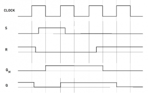
What is Inductive Reactance: 29 Important Facts

Inductor:

An inductor is a passive component of an electrical circuit that opposes current. It is a coil of wire wrapped around a magnetic material. Applied voltage induces current across the inductor. When current flows through the inductor, it generates a magnetic field. Magnetic fields don’t change. Therefore, the inductor tries to prevent the current flowing through it from changing.
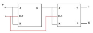
Reactance:

Reactance is defined as an opposition to current flow in an electrical circuit. It is denoted by ?

Inductive Reactance XL:

Inductive reactance is the reactance offered by an inductor: the greater the reactance, the smaller the current. 

In a dc circuit inductive reactance would be zero (short-circuit), at high frequencies an inductor has infinite reactance (open-circuit).

Inductive Reactance Units | SI unit of inductive reactance

Inductive reactance acts as an opposition to the current flow in the circuit. So the SI unit of inductive reactance is the same as that of resistance, i.e. Ohms. 

Symbol for Inductive reactance

Inductive reactance is denoted by ?L or XL

Derivation of Inductive Reactance 

Circuit for derivation of Inductive Reactance

Suppose we have the following electric circuit with inductance L connected to an AC voltage source. This source creates an alternating current that flows inside the inductor if the switch is closed. So, the electric current in the circuit at any moment is given by,

I=IOCosωt

Where I0= peak value of the current

           ω= angular frequency

Now, if we apply Kirchhoff’s second law or Kirchhoff’s loop law in this circuit, we get,

ezgif 4 ee9433e7d4
ezgif 4 5d485d189f

So, the voltage across the inductor V is equal to the inductance multiplied by the derivative of electric current I with respect to time. 

ezgif 4 43bf5c47bb
ezgif 4 d63bca6098

If  cos(ωt+90°)= 1, then V=V0=LI0ω (peak voltage)

We know by Ohm’s law, 

Inside a resistor, 

V0=I0

where R= resistance

V0=I0\\XL   

As the inductive reactance is similar to resistance, we can get an analogous equation-

where ?L=inductive reactance

By comparing V0 found in the previous equation, it can be concluded that,

XL = ωL = 2πfL

where f=frequency

Inductive Reactance formula

The inductive reactance of a coil is,

?L=ωL or ?L=2?fL

Where ω is the angular frequency, f is the frequency of the applied voltage, and L is the inductance of the coil.

Derivation of Inductive Reactance

Inductive reactance in series

Inductors in series

In the above circuit, three inductances L1, L2 and L3 are connected in series. Therefore, if we apply Kirchhoff’s law,

ezgif 4 5ee6a7b067
ezgif 4 0ce8f4f7b2

Taking the peak value, we can say that,

Vo = Ioω(L1 + L2+ L3)

So, total inductance L=L1+L2+L3

Therefore, inductive reactance in series connection, ?L(L1+L2+L3+…..Ln)

Inductive reactance in parallel

Inductors in parallel

In the above circuit, three inductances, L1, L2 and L3, are connected in parallel. If the total inductance is L, by Kirchhoff’s law, we can say,

ezgif 4 bd58fa6028

So,

ezgif 2 65846567eb

Therefore, inductive reactance in parallel connection,

ezgif 2 c6fdb646eb

Inductance and inductive reactance

Magnetism and electricity co-exist in electrical circuits. If a conductor is placed in a continuously changing magnetic field, a force is generated in the conductor. It is called the electromotive force or EMF. The ability to create voltage for the change in current flow is called inductance

EMF helps the current flow in the circuit. While current passes through the inductor coil, it tries to oppose the current. This reaction is known as inductive reactance.

What is the difference between inductance and inductive reactance ?

Inductance

  • Inductance:
ezgif 3 564f230c9b
  • Unit of inductance is Henry or H.
  • Dimension of inductance is [ML2T-2A-2]
  • It does not depend upon frequency.
  • The greater the inductance, the more the induced EMF and current will be.

Inductive reactance

  • Inductive reactance XL=ωL.
  • Unit of inductive reactance is ohm or Ω.
  • Dimension of inductive reactance is [ML2T-3I-2].
  • It is dependent upon frequency.
  • The greater the inductive reactance, the lesser the current will be.

Inductive Reactance in DC circuit

In a DC circuit, power frequency is equal to zero. Hence ?L is also zero. The inductor would behave like a short circuit in the steady-state.

Relation between inductance and reactance

Reactance ? consists of two components-

  • Inductive reactance or ?L
  • Capacitive reactance or ?C

Therefore

Total inductive reactance formula

ezgif 2 15b6b02082

Difference between inductance and reactance

Inductance:

ezgif 3 564f230c9b 1
  • Unit of inductance is Henry or H.
  • Dimension of inductance is [ML2T-2A-2]
  • It does not depend upon frequency.
  • Inductance is directly proportional to current.

Inductive reactance

  • Reactance
ezgif 3 fc55c6c471
  • Unit of reactance is ohm or Ω
  • Dimension of inductive reactance is [ML2T-3I-2]
  • It is dependent on frequency. 
  • Reactance is inversely proportional to current.

The inverse of inductive reactance is susceptance

The quantity reciprocal to inductive reactance is known as inductive susceptance. It is denoted by BL

ezgif 2 1bbabe2d50

Inductive susceptance is similar to conductance G, which is the inverse of resistance.

So the unit of BL is also siemen or S.

Physically inductive susceptance represents the capability of a purely inductive electrical circuit to allow the flow of current through it.

Reactance and susceptance 

Reactance measures a circuit’s reaction against the change in current with time, while susceptance measures how susceptible the circuit is in conducting the varying current.

Resistance, reactance, capacitance, inductance impedance-comparison 

ParametersResistanceReactanceCapacitanceInductanceImpedance
DefinitionThe measure of obstruction caused by the conductortowards the current is known as resistance.The characteristic of the inductor and the capacitor to oppose any change in current is called reactance.The capacity of a conductor to store electric charge is known as capacitance.The property of a conductor to generate an EMF due to the change in current is known as inductance.Impedance is the entire opposition in an electrical circuit caused by the inductor, the capacitor and the resistor.
SymbolResistance is represented by RReactance is represented by ?Capacitance is represented by CInductance is represented by LImpedance is represented by Z
UnitOhmOhmFaradHenryOhm
General ExpressionResistance in a circuit with voltage v and current i is, R = V/IReactance in a circuit with voltage source’s angular frequency ω is, X= ωL + 1/ωCThe capacitance of a parallel plate capacitor with medium permittivity ϵ, A plate area and d separation between plates is, C=ϵA/dThe inductance of a coil with induced voltage V is, L=V/ dI/dTThe total impedance of a circuit can be written as Z=ZR+ZC+ZL

Capacitive reactance

Just like the inductive reactance, capacitive reactance is the impedance caused by the capacitor. It is denoted by Xc. When DC voltage is applied in an RC circuit, the capacitor starts charging. Subsequently, current flows, and the capacitor’s internal impedance obstructs it. 

Capacitive reactance

ezgif 2 ad1ef3f728

What is the difference between inductive reactance and capacitive reactance ?

Capacitive Reactance vs Inductive Reactance

Capacitive reactanceInductive reactance
The reactance of the capacitorThe reactance of the inductor
It is denoted by XCIt is denoted by XL
XC =1/ωCXL =ωL
When a sinusoidal AC voltage is applied to a capacitor, the current leads the voltage by a phase angle of 90°When a sinusoidal AC voltage is applied to an inductor, the current lags the voltage by a phase angle of 90°
It is inversely proportional to the frequency.It is directly proportional to the frequency
In DC supply, the capacitor behaves like an open circuit.In DC supply, the inductor behaves like a short circuit.
At high frequency, the capacitor acts as a short circuit.At high frequency, the inductor acts as an open circuit.

AC circuit in LR series combination

LR circuit

There are two components in the above circuit- resistor R and inductor L. Let the voltage across the resistor is Vr, and the voltage across the inductor is VL.

The phasor diagram shows that total voltage V, resistor voltage Vr and inductor voltage VL forms a right-angled triangle.

By applying Pythagoras theorem, we get,

V2=Vr2+VL2

ezgif 2 eb4498d733

where φ=phase angle

How to find inductive reactance ? | Important formulas

XL = 2πfL

ezgif 2 b4d2ff548a
ezgif 2 52bf757927

Power P=VrmsIrmsCosφ

Calculate the inductive reactance | Inductive reactance calculation example

Find the AC voltage required for 20 mA current to flow through a 100 mH inductor. Supply frequency is 500 Hz.

Circuit 1 with 100 mH inductor

Given: i= 20 mA   f=400 Hz    L=100mH

As the series is purely inductive, the impedance in the circuit, Z=XL

We know, XL=ωL=2?fL=2 x 3.14 x 400 x 0.1=251.2 ohm

Therefore, supply voltage V=iXL= .02 x 251.2= 5.024 volts

Calculate XL of a 5 mH inductor when 50 Hz Ac voltage is applied. Also find Irms at each frequency when Vrms is 125 volts.

XL=2?fL=2 x 3.14 x 50 x 5 x .001 = 1.57 ohm

ezgif 3 03802bdc1a

Calculate inductive reactance using voltage and current

A resistance of 20 ohm, inductance of 200 mH and capacitance of 100 µF are connected in series across 220 V, 50 Hz mains. Determine XL, XC and current flowing through the circuit.

RLC circuit

We know, V=220 volt  R=20 ohm  L=0.2 H   f=50 Hz

XL=2?fL=2 x 3.14 x 50 x 0.2=62.8 ohm

ezgif 3 38f20f8cb8

=1/(2 x 3.14 x 50 x 0.0001)=31.8 ohm

Therefore total impedance,

ezgif 3 6ff5f06bbf 1

= (20)2+(62.8-31.8)2=36.8 ohm

So, current

ezgif 3 02ab9d3709

Resistance-Reactance-Impedance: Comparative study

ResistanceReactanceImpedance
Opposes electron flowOpposes change in currentCombination of reactance and resistance
R=V/IX=XL + XCZ=(R2 + XL2)1/2
Measured in ohmMeasured in ohmMeasured in ohm
Does not depend upon frequencyDepends upon frequencyDepends upon frequency

Leakage reactance in induction motor

Leakage reactance is the impedance caused by the leakage inductor in an induction motor. A rotating magnetic field develops in the induction motor due to the applied 3-phase power. Most of the magnetic flux lines generated by the stator winding travel across the rotor. Though a very few flux lines close in the air gap and fail to contribute to magnetic field strength.This is the leakage flux.

Due to this leakage flux, a self-inductance is induced in the winding. This is known as leakage reactance.

Sub-transient reactance of induction motor

In a short circuit, the magnetic flux generated in the damper winding reduces steady-state reactance. It is known as sub-transient reactance. The term ‘sub-transient’ suggests that the quantity operates even faster than the ‘transient’. 

FAQs

To what is inductive reactance proportional? 

Inductive reactance is directly proportional to the frequency.

What is inductive reactance and how does it affect an AC circuit ?

Unlike DC, in the AC circuit, the current varies with respect to time. 

What happens when the capacitive reactance is greater than the inductive reactance?

If XC is more than XL, then the overall reactance is capacitive. 

What is induction?

The change in magnetic field causes voltage and current in the circuit. This phenomenon is known as induction

What does inductance do in a circuit?

Inductance opposes the change in current flowing through the circuit.

What is inductance of a coil?

The inductance of a coil originates from the magnetic field due to varying current.

Why is L used for inductance?

According to the initials, I should have been used for representing inductance. But as I is already being used for current, L is used for inductance to honour scientist Heinrich Lenz for his extraordinary contribution in the field of electromagnetism. 

Can self inductance be negative?

Self-inductance is purely a geometric quantity, and it depends upon the external circuitry. Therefore it cannot be negative. The minus sign in Lenz law indicates the opposing nature of EMF towards the magnetic field.

Do Motors have inductance?

Back EMF is a crucial factor in motors. Both AC and DC motors make use of a low AC voltage source to measure inductance.

What is unit of inductance?

SI unit of inductance is volt -second per ampere or Henry.

Why does inductor block AC and allows DC?

The inductor creates an EMF when current flows through it. In AC, the EMF is very high as the frequency is increased. Therefore the opposition is also significant. But in DC supply, there’s no EMF, and consequently no opposition takes place. So it is said that the inductor blocks AC and allows DC.

Does inductor allow DC current?

Inductor allows DC current as there’s no opposite force acting in the circuit.

For more details about circuit theory click here

Combinational Logic: 21 Important Facts You Should Know

33342206026 2ff95d1cc3 b

Combinational Logic Definition

Combinational logic is a type of logic in which the output can only be modified by present input.

Combinational Logic Circuits| What is Combinational Logic Circuit

Combinational circuitry is a type of circuitry in which the current input can only modify the current output.  This circuit is also known as the clock independent circuit because for operation is doesn’t need a clock. This circuit doesn’t have a memory element or any feedback path, so the circuit can’t store any data. A combinational circuit can design by combining the logic gates. The circuitry used in combinational logic is used as coding, decoding, error detection, manipulation, etc. The basic circuits of combinational logic are multiplexer, decoder, encoder, shitter, Adder, Subtractor, etc.

image 2 1 2

Fig. Block diagram of a combinational circuitry.

A combinational logic circuit can have ‘n’ number of input variables and ‘m’ number of the output variable. For the ‘n’ input variable, there is 2n possible combinations of input variables. For each unique combination of input variables, there is only one possible output combination. The output function is always expressed in terms of the input variables. A truth table or Boolean equation can determine the relationship between the output and input of a combinational circuit.

Types of Combinational Logic Circuits

The classification of the combinational circuitry is based on the application they being used:

  1. Arithmetic and Logical circuit: Adder, Subtractor, Comparators, etc.
  2. Data Transmission: Multiplexer, Demultiplexer, Encoder, etc.
  3. Code Converter: Binary code converter, BCD code converter, etc.

Combination Logic Gates

Combinational logic gates are the fundamental gate which is combined to form any circuitry in the digital electronic. A logic gate is ideal for implementing an essential Boolean function—for example, gate, NAND gate, OR gate, NOR gate, etc.

Combinational logic gates
Image credit: “Logic gates” by Plusea is licensed under CC BY 2.0

AND gate:

AND gate has two or more input with one output. The output is high means ‘1’ when all the input is high; otherwise, the outcome is low means ‘0’.

image 3 2

Fig. Logic diagram of AND gate

OR gate:

OR gate has two or more input and one output. The output is high means ‘1’ when at least one input is high; otherwise, the result is low, which means ‘0’. But in commercial OR gate with 2,3 and $ input types is available.

image

Fig. Logic diagram of OR gate

NOT gate:

NOT gate has one input with one output. When the input is high means ‘1’, then the NOT gate’s output will be low, which means ‘0’.

image 4 1

Fig. Logic diagram of NOT gate

NAND gate:

NAND gate means NOT AND, here AND gate output feeds into NOT gate. NAND gate can be designed from the AND gate truth table by complementing the output variables. The result of the NAND gate is low when all the logic input ishigh. Otherwise, the output is high.

image 5 1

Fig. Logic diagram of NAND gate

NOR gate:

NOR means NOT OR gate. Here OR gate output is feed into NOT gate. NOR gate designed from the OR gate truth table by complimenting all the output variables. The output of a NOR gate is high when all inputs are low. Otherwise, the output is low.

image 6 1

Fig. Logic diagram of NOR gate

XOR gate:

XOR gate means Exclusive-OR gate, also known as EX-OR gate, it has two input and one output. For two input gates, the output of the XOR gate is high, which means ‘1’ when the input bit is unlike, and output is low means ‘0’ when there is like input.

image 7 1

Fig. Logic diagram of XOR gate

XNOR gate:

XNOR means Exclusive-NOR gate, also known as EX-NOR; it is NOT of EX-OR. The output of a two-input XNOR gate is high, which means ‘1’ when the input is like and Low when, unlike input.

image 8 1

Fig. Logic diagram of XNOR gate

Combinational Logic Examples| Combinational Logic Circuits Examples

Half Adder:

Half adder is an example of combinational circuitry, in which we can add two bits. It has two input, each of one bit and two output, in which one is carry output, and the other is for sum output.

image 9 1 1

Fig. Logic diagram of half adder designed with AND gate and XOR gate.

Full adder:

Full adder is an example of the arithmetic combinational circuit; here, we can add their bit at a time, and has two output sum and carry. In half adder, we could only add two bits at a time. A full adder overcomes that limitation; a full adder is essential for adding a huge binary number. However, one full adder can add an only one-bit binary number at a time, but by cascading the full adder, we can add a more extensive binary number. However, we can create a full adder by combining two half adders.

image 10 2

Fig. Block diagram of full adder

Half Subtractor:

A half subtractor is an arithmetic combinational circuit that performs subtraction of two input bit and provides two outputs, one as a difference and the other as borrow. Designing the subtractor circuit is mainly similar to that of an adder. I cannot consider any borrow input.

image 11 1

Fig. Logical diagram of half subtractor designed with AND gate, NOT gate and XOR gate.

Full Subtractor:

Full subtractor is also an arithmetic combinational circuitry, where we can perform subtraction of three one-bit inputs, inputs are the minuend, subtrahend, and a borrow. It generates two outputs, one as the difference of the input and the other as borrow.

image 12 1

Fig. Block diagram of full subtractor.

Multiplexer:

The multiplexer has multiple inputs and a single output, and it has a selector line that selects one input at a time as the requirement. It sends it to the output line, and for the ‘n’ number of input here, we need the ‘m’ number of the select line where n = 2m. It also has an enabled input line, enabling us to cascade multiplexer or further expansion as required.  It is also called a data selector.  16: 1 Is the largest multiplexer available in IC form.

image 13 2

Fig. Block diagram of Multiplexer.

Demultiplexer:

Demultiplexer has only one input and multiple outputs. It has a selector line that selects one output line at a time; with the select line, we can distribute the input signal into many output lines as our requirement. For the ‘n’ number of output line here, we need the ‘m’ number of the select line where n = 2m. Demultiplexer can work as a binary to decimal converter.

image 14 2

Fig. Block diagram of Demultiplexer.

Comparator:

A comparator is a combinational circuit where it can compare the magnitude of a two n-bit number and provide us with the relative result as output. It can have three outputs. For example, the input we provide A and B to the comparator where A and B can be an n-bit number the output of the comparator can be A<B, A=B, A>B. The circuit checks the magnitude of the input and compares it; there is a different output port for A=B, A>B, and A<B. When the comparing of the magnitude is done, the respective output get. As a result, the output can be active low or active high depends on the circuitry.

image 15 1

Fig. block diagram of n-bit comparator

Encoder:

The encoder is a combinational circuit. It has 2n input lines and has ‘n’ output lines corresponding to the n-bit code input.

image 16 1

Fig. Block diagram of Encoder.

Decoder:

It is a circuit that converts binary n input lines to a maximum 2n output lines.

image 17 1

Fig. Block diagram of a decoder.

BCD adder:

A BCD adder is an arithmetic combinational circuit used to operate addition on BCD numbers, digits and produced output in BCD form. Sometimes the output of a BCD adder may be a valid BCD number, and then it converts that invalid BCD number into valid by adding 0110 to the invalid output.

BCD subtractor:

A BCD subtractor is to operate the subtraction on the BCD number. If we take two input BCD number, one as A and the other as B, subtraction of the BCD number is equivalent to the addition of a compliment of B to A. In BCD, subtraction 9’s complement or 10’s complement method is used.

ALU (Arithmetic Logical Unit):

 The circuitry of the Arithmetic logical unit is widely used as a combinational circuitry, and This circuitry is used to perform all the arithmetic and logical operation for and processor. ALU is known as the heart of a microprocessor or microcontroller.

File:ALU block.gif
Image Credit: “File:ALU block.gif” by Lambtron is licensed under CC BY-SA 4.0

Combinational Logic with MSI and LSI

MSI stands for “Medium-scale integration”, it can contain 30 to 1000 electronic components in a single chip of IC. LSI stands for “Large scale integration”, It can have thousands of embedded components and integrated on a single IC.

Adder with MSI and LSI:

TRUTH TABLE:

ABCSC
00000
00110
01010
01101
10010
10101
11001
11111

Equation for sum:

S=AB’C+A’BC+AB

Carry:

C=AB’C+A’BC+AB

image 18 2

Fig. Implementation of Full-Adder in MSI or LSI circuitry.

Combinational Logic Design |Design a Combinational Logic Circuit

The Objective of Designing Combinational logic:

  • To get desired output from the circuitry.
  • An economic circuitry means with minimum expenses building a circuitry.
  • The complexity of the circuitry must be reduced as much as possible.
  • With a minimum number of gates, a digital circuit should be designed to minimize the overall circuit delay.

The combinational circuit can be designed with the multiplexer, procedure for designing:

  • Determine the number of input and output variables of the required circuit.
  • Get the truth table or logic diagram of the required circuit.
  • From the truth table or logic, the diagram determines the Boolean expression of the required circuit and expands it into minterms, and each defines a unique data line of the multiplexer.
  • For ‘n’ number of input, variables get 2n to 1 multiplexer.
  • With the help of a select line and input, you can get output from the multiplexer according to your desired circuit.

Combinational Circuit Design Using Logic Gates

Designing a combinational logic circuit can be done with gates, whereas gates are practically available as IC. For different gates, there are other IC available with different IC numbers.

Steps or procedure to get the required combinational logic circuit:

  • Determine the number of input or output variables required for the operation through the given truth table, Boolean statement, or expression.
  • Derive the expression in the form of a sum of product (SOP) or product of sum (POS).
  • Reduce the expression using the Boolean reduction method or K-map.
  • You can design the circuit with the required number of gates in the logic diagram through the reduced expression.

Functions of Combinational Logic

The functions of a combinational logic can be defined with Truth Table, Logic Diagram or Boolean Equation.

Truth Table: Truth table is a tabular list of all possible binary combinations of the input variable and related output combination of a logic circuit. There are only two possibilities of an input or output bit, i. e. ‘0’ and ‘1’. If the number of input is ‘n’, there will be 2n combinations. In this table, there is one row for representing input combinations as well as different rows for output combinations. This can be obtained from the logic diagram or Boolean expression of the circuitry.

Logic Diagram: The logic diagram is mainly composed of a basic logic gate and some symbolic representation of the circuit. It shows us the interconnection of logic gates, represents some signal lines (like enable, select line, control lines, etc.). It is used to define the functionality of circuitry. It can be obtained through Boolean expression or the truth table of the circuitry.

Boolean Expression: This is an equation formed from the combination of input and output variable; here, the expression is mainly used to define the input variable’s output variable. This expression can be derived from the truth table or the logic diagram of the circuitry.

Combinational Logic Circuit Real Life Examples

In real life, we can see the combinational circuit in calculator, RAM (Random Access Memory), Communication system, Arithmetic and logic unit in CPU (central processing Unit), Data communication, wi-fi, cell phone, Computer, etc. These are a real-life example of where the combinational circuit is used.

Analysis Procedure in Combinational Logic

Combinational circuit analysis is the analysis of a given logic circuit or a circuit diagram; from here, we can gather information regarding the circuit. An analysis is to verify the behaviours of the circuitry with its specifications; analysis of a circuit can be used to reduce the number of gates, optimise, reduce delay, or convert the circuit into another required form.

Analysis procedure of combinational logic:

  • Determine the output variable of the circuitry, and try to get a truth table or logic diagram of the circuit with input and output variables.
  • Through a truth table or logic diagram of the circuitry, define the Boolean function with the help of input and output variables.

Verilog for Loop Combinational Logic

What is a combinational loop?

The combinational loop is a loop in which the output of a combinational logic(which can consist of one or more combinational logic gates) is feedback to the same logic without any memory element in the feedback path.

Types of the combinational loop:

  • Not equivalent to latch
  • Equivalent to latch
image 19 1

Fig. Combinational loop type latch

Verilog for loop combinational logic:

If(sel==1’b0)

Y=I0;

else

Y=Y;

Here combinational loop implemented, which is equivalent to latch.

CMOS Combinational Logic Circuits| Combinational Logic Networks

Static CMOS is widely used for circuitry because it has good performance, low power consumption. A CMOS gate is a combination of a pull-up network (PUN) and Pull-down network (PDN); an input is distributed to both pull-up and pull-down circuits.

The function of the pull-up network is to connect the output with the voltage source when the output needs to be ‘1’. Whereas a pull-down network provides the connection between the ground to the output when the output is meant to be ‘0’. Pull-down network is designed with NMOS, and PMOS is used in PUN. NMOS is connected in series to form AND function, whereas when connected in parallel from OR function. Where PMOS in parallel form output as NAND function and series form NOR function.

image 20 2

Fig. CMOS diagram of half adder.

 CMOS is a complementary network. This means for parallel connection in pull-up network there is the series connection in pull-down network. The complementary gate is generally inverting. With one stage, it can perform a function such as NAND, NOR, and XNOR, and for non-inverting Boolean function such as AND, OR and XOR, it required an extra inverter stage. The number of transistors for implementation of n- input logic gate is 2n.

MUX Combinational Logic

MUX i.e., Multiplexer is a combinational logic design, it has only one output and can have multiple input. It has ‘n’ select line for2n input, selector line s use to select which input line will be connected to the output line.

image 13 1

Fig. Block diagram of a 4:1 multiplexor

TRUTH TABEL OF 4:1 MULTIPLEXOR:

S1S2Y
00I0
01I1
10I2
11I3

Simple Combination Lock Using Logic Gates

A simple combinational look is a circuit designed with XOR and NOR gate, where XOR gate is a bit comparator, and NOR gate is used as a controlled inverter. We can use XOR to check and compare the input and the key code bit by bit; if the input completely matches with the key code, the lock will be unlocked. When the inputs and not the same XOR provide ‘1’ as an output, now the output will go through the NOR gate. In this way, we can design a simple lock using gates.

Combinational Logic Circuits Applications

Combinational logic circuits are the basic circuit in digital electronic even sequential circuit is designed from the combinational circuit with the memory element.

These circuits are used for designing the ROM of a computer or a microprocessor. ROM (Read Only Memory) is designed with Encoder, Decoder, Multiplexer, Adder Circuitry, Subtractor Circuitry, etc., which are all combinational circuits.

Whereas ALU (arithmetic and logic unit) in the processor, which is also from the combinational circuit, mainly consists of Adder, Subtractor, etc., to perform every arithmetic operation.

Encoder and decoder are used to convert one form of data to another (like from Binary to Decimal); these are commonly used in communication for transferring data from one end to another. This circuit provides synchronization if needed; with the help of these, we can perform any operation with greater accuracy.

A multiplexer is used to transfer data in a single line. This circuit is used in broadcasting, telegraphy, etc.

Disadvantages of Combinational Logic Circuits

The limitation or disadvantage of half-adder is overcome by a full adder, whereas the full subtractor overcomes the restriction of half subtractor.

Disadvantages of Multiplexer: Limitation of using the port, which can use in a specific sequence. The circuitry can cause delay.

The disadvantage of Demultiplexer: wastage of bandwidth, delay can from due to synchronization.

Disadvantages of Encoder: Complex circuitry can be easily subjected to magnetic interference.

Overall, the combinational circuit is complex as the circuit is getting bigger; in bigger circuitry, there can be high propagation delay, it doesn’t have any memory element.

Combinational logic circuits MCQ | Combinational logic circuit problems and solutions | FAQ

What is combinational logic What are its characteristics ?

Described in Combinational logic circuit section.

What is 1*4 Demultiplexer in Combinational Logic Circuits ?

A 1 to 4 Demultiplexer has two select line, four output and one input. The input data connected to the output line according to the select line.

image 14 1

Fig. Block diagram of 1:4 Demultiplexer

Truth Table:

INPUTS   OUTPUTS 
S1S0Y3Y2Y1Y0
000001
010010
100100
111000

Can you ever have metastability with pure combinational logic ?

Yes, there can be a metastability state for some time in pure combinational logic.

             Metastability refers to the state which cannot be defined as ‘0’ or ‘1’. Usually, this happens to a circuit when the voltage is stuck between ‘0’ and ‘1’, which can cause oscillation, uncertain output, unclear transition, etc. When such a signal goes through the combinational circuit, it can violate basic gates’ specification and spread through the overall circuit.

For example, when taking the given circuit, as we see here, there is an AND gate and a NOT gate, practically a circuit has some propagation delay; as AND gate has some propagation delay, the NOT gate has to. As we know, the output should be defined at all times, but there is a time interval T where the output state or the transition state is not definite or undesirable. That state at that time interval can be considered as metastability of a pure combinational logic circuit.

Design consideration of different combinational logic circuits in VHDL.

For designing circuitry, you must know the basic of VHDL, such as representing a Boolean function, representing a fundamental gate, etc.

Here we considering full-adder as an example:

In VHDL:

Entity FullAdder is

Port (A, B, C: in bit;

D, S : out bit);

end FullAdder

Advantages of design and testing of combinational logic circuits using self in test scheme

Advantages:

  • Lower cost for testing.
  • Fault can be easily detected.
  • Shorter test time.
  • For higher reliability on the circuit, a self-test scheme s used.

What is the diffrence between combinational and sequential logic ciruit?

To know about sequential logic click here.

What is Avalanche Photodiode ? | Its 5+ Important uses and characteristics

Avalanche Photodiode

Avalanche Photodiode Definition

Avalanche photodiodes or APDs are highly sensitive semiconductor devices that transform optical signals into electrical signals. These are operated under high reverse bias. The term ‘avalanche’ comes from the avalanche breakdown phenomenon.

Avalanche Photodiode Symbol

Avalanche Photodiode

The symbol of avalanche photodiode is the same as that of Zener diode.

Avalanche Photodiode structure

APD structure

The structure of the ordinary Avalanche photodiode is similar to the PIN photodiode. It consists of two heavily doped (p+ and n+ region) and two lightly doped (I or intrinsic region and P region) regions. The width of the depletion layer in the intrinsic region is relatively thinner in APD than the PIN photodiode. The p+ region acts like the anode, and n+ acts like the cathode. Reverse bias is mostly applied across the pn+ region.

Avalanche photodiode Circuit Diagram

For applying reverse bias conditions, the p+ region is connected to the negative terminal, and the n+ region is connected to the battery’s positive terminal.

Avalanche photodiode working principle

  • Avalanche breakdown takes place when the diode is subjected to high reverse voltage.
  • The reverse bias voltage increases the electric field across the depletion layer.
  • Incident light enters the p+ region and further gets absorbed in the highly resistive p region. Here electron-hole pairs are produced.
  • A comparatively weaker electric field causes separation between these pairs. Electrons and holes drift with their saturation velocity towards the pn+ region where a high electric field exists.
  • As the velocity is maximum, the carriers collide with other atoms and generate new electron-hole pairs. A large number of e-h pairs results in high photocurrent.

Avalanche photodiode Characteristics

  • The intrinsic region in APD is slightly p-type doped. It is also called ?-region.
  • The n+ region is thinnest, and it is illuminated through a window.
  • The electric field is maximum at the pn+ junction, and then it starts decreasing through the p region. Its intensity lessens in ?-region and gradually vanishes at the end of the p+ layer.
  • Even a single photon absorbed leads to the generation of a vast number of electron-hole pairs. This is called the internal gain process.
  • Excess electron-hole pair generation due to the collision of charge carriers is called avalanche multiplication. Multiplication factor or gain,

M=Iph/Ipho

Where iph= multiplied APD photocurrent

            ipho=photocurrent before multiplication

M value strongly depends upon reverse bias and temperature also.

Avalanche Photodiode Operation

APDs are operated in completely depleted mode. Besides the linear avalanche mode, APDs can also work in the Geiger mode. In this mode of operation, the photodiode is operated at a voltage above breakdown voltage. Recently another mode has been introduced, which is called Sub-Geiger mode. Here along with single-photon sensitivity, the internal gain is also very high, just below the breakdown.

Impact ionization in Avalanche Photodiodes 

After the photons are absorbed in ?-layer, a sufficient number of electron-hole pairs are formed. The electric field separates the pairs, and the independent charge carriers run towards the n+ and p+ regions. In the p region, the electrons experience a massive electric field. In the effect of this field, electrons drift with their saturation velocity and collide. This collision helps in charge multiplication. This overall phenomenon is called impact ionization.

Ionization rate, k=α/β

Where ⍺= rate of electrons

            ꞵ= rate of holes  

Avalanche Photodiode Diagram

Avalanche Photodiode Datasheet

PhotodetectorWavelengthResponsivityDark Current
InGaAs APD1310-1550 nm0.8 A/W30 nA
Germanium APD1000-1500 nm0.7 A/W1000 nA

Avalanche Photodiode Module

APDs are part of modules that contain additional electronic elements apart from the photodiode. There can be a trans-impedance op-amp in some packages that improve the performance and increases bandwidth and responsivity. Some packages are optimized to be used in optical fiber. Some incorporate thermosensors to provide better stability.

Avalanche Photodiode Array

Avalanche photodiode arrays are small in size and also yield lease gain. These are designed especially for use in LIDAR, laser rangefinders, etc. Although APD arrays are not mainstream products yet, some manufacturers are making these due to their unique features.

Avalanche Photodiode Noise

The primary components of noise in APD are 

  • Quantum or shot noise (iQ): The avalanche process is the primary reason behind this. 
  • Dark current noise: Dark current noise is generated from the absence of light in a photodiode. It can further be classified into bulk current noise(iDB) and surface current noise(iDS).
  • Thermal noise: It is the noise of the amplifier connected to the photodiode.

Due to carrier multiplication, significant noise is added to the existing noises. It is known as excess noise factor or ENF.

ENF or F(M)= kM + (2-1/M)(1-k)

Where M = multiplication factor

            k = impact ionization coefficient

Therefore the mean square value of total noise iN in APD is,

gif 1 2

Where 

q= charge of an electron

Ip= photocurrent

B= bandwidth

M= multiplication factor

ID= bulk dark current

IL= surface leakage current

Thermal noise in trans-impedance amplifier is,

gif 9

Where kB= Boltzmann constant

           T= absolute temperature

           RL= load resistance

Difference Between PIN and Avalanche Photodiode | Avalanche Photodiode vs. PIN Photodiode

Avalanche PhotodiodeParametersPIN Photodiode
Four layers- P+, I, P, N+LayersThree layers- P+, I, N+
Very highResponse timeVery less
Low value of currentOutput currentCarrier multiplication causes amplified current value
Gain can be as high as 200Internal gainGain is insignificant
Highly sensitiveSensitivity Slightly less sensitive
Amplifiers can improve the performance, but APD can still function without this as the gain is already there.Amplifier No internal gain is there, so the use of amplifiers is mandatory.
Higher due to charge multiplicationNoiseComparatively lesser than APDs
Extremely high Reverse Bias voltageLow 
Great Temperature stabilityPoor

Avalanche Photodiode Amplifier

Like PIN photodiodes, APDs also use the four-channel trans-impedance amplifier for reduced noise, high impedance, and low power consumption. Some amplifiers offer temperature flexibility and high reliability also. All these characteristics make the photodiode suitable for use in LIDAR receivers.

Avalanche Photodiode detector

APDs are preferred over PIN photodiodes in light detection for their increased sensitivity. As a relatively high voltage is given, the number of charge carriers overgrows, and they are accelerated in the effect of strong electric fields. The internal collision occurs, and charge multiplication takes place. As a result, the photocurrent value rises, which improves the overall photo-detection process.

Avalanche Photodiode in optical fiber communication

In optical fiber communication systems, APDs are usually needed for the detection of weak signals. Circuitry must be optimized enough to detect the weak signals maintaining a high SNR(Signal to noise ratio). Here,

SNR=(power from the photocurrent/power of photodetector) + power of amplifier noise

For achieving a good SNR, quantum efficiency must be high. As this value is nearly close to the maximum value, most of the signals are detected.

Comparison between APD and PMT | Avalanche Photodiode vs Photomultiplier tube

Avalanche PhotodiodePhotomultiplier Tube 
It consists of four layers with different doping concentrations.It consists of a photocathode, dynodes, and a vacuum glass tube.
It uses the avalanche multiplication phenomenon to produce charge carriers.It uses the photon absorption technique for the emission of excess electrons.
It converts photons into electrons.It amplifies the number of electrons.
APDs are highly sensitive.The sensitivity of PMT is limited.
The cost of APDs is lower than that of PMTs.PMTs are the costliest devices.

APDs and quenching circuits 

  1. Passive quenching circuit: This type of circuit uses a load resistor, a passive element, to quench the breakdown pulse. Photoelectrons trigger the avalanche. A large current is passed through the circuit to avoid the shortage of electrons or holes in the avalanche region, and the diode remains in conducting state.
  1. Active quenching circuit: While the diodes are recharged, the probability of another photoelectron striking it is very low. To minimize the dead-time, ‘active quenching’ is done. The bias voltage is temporarily dropped, and this delay allows the collection of all electrons and holes. When again the voltage is increased, no electron remains at the depletion region.

InGaAs Avalanche Photodiode

InGaAs or Indium Gallium Arsenide is vividly used in semiconductor devices. InGaAs avalanche photodiodes are used for achieving long-reach optical fiber communications. These can perform photo-detection in the range of 1100-1700 nm. InGaAs avalanche photodiodes are better than ordinary germanium avalanche photo diodes in terms of SNR and sensitivity.

Large area avalanche photodiode

Large area APDs or LAAPDs are lightweight photodiodes that possess a large activation area. Its features include fast response time, improved SNR, insensitivity to magnetic fields, etc.

UltravioletUV Avalanche photodiode

Ultraviolet avalanche photo diodes offer outstanding sensitivity if operated in Geiger mode. The silicon carbide UV APD shows a high signal gain and extreme sensitivity. UV APDs are ideal for ultraviolet flame detection.

Silicon Avalanche Photodiode

High silicon APDs are great for low light detection. Internal multiplication features great photosensitivity that makes it capable of detecting low light signals. It also has improved linearity, low terminal capacitance, and low-temperature coefficient. Some applications of Si avalanche photo diodes are optical rangefinders, laser radars, FSO, etc. 

Silicon Avalanche Photodiode array

In multi-element silicon APDs, the depletion region is fabricated just below the photosensitive area. Due to this, the APD array multiplies the incident light. The charge carriers struck in the depletion region. This implies that Si avalanche photo diode arrays have low crosstalk because of the gain.

Geiger mode avalanche photodiode

Geiger mode avalanche photo diodes are developed to provide an alternative to the photomultiplier tubes. GAPDs use the single-photon counting principle at a voltage little more than the threshold breakdown voltage. At this voltage, even a single electron-hole pair is capable of triggering a strong avalanche. In this situation, the quenching circuits reduce the voltage by a fraction of a second. This stops the avalanche for the time being, and photo-detection is possible.

Photon counting techniques with silicon avalanche photodiodes

Over the years, two types of photon counting techniques are being used in avalanche photo diodes. 

  • Geiger mode
  • ‌Sub-geiger mode

Studies suggest that the Geiger mode improves the performance excellently for using quenching circuits.

Single photon avalanche photodiode | Single Photon counting Avalanche Photodiode

These are also called SAPD. SAPDs are highly photosensitive and optimized for high quantum frequency. Some of its applications include an image sensor, 3D imaging, quantum cryptography, etc.

Advantages and Disadvantages of Avalanche Photodiode

Advantages of Avalanche Photodiode

  • ‌It can detect light of low intensity.
  • ‌Sensitivity is high.
  • ‌Response time is faster.
  • ‌A single photon can generate a large number of electron-hole pairs.

Disadvantages of Avalanche Photodiode

  • ‌High operating voltage is required.
  • ‌Excess noise due to carrier multiplication.
  • ‌Output is not linear.

Application of Avalanche Photodiode

  • LASER scanner.
  • ‌Barcode reader.
  • ‌laser Rangefinders.
  • ‌Speed gun.
  • ‌Laser microscopy.
  • ‌PET scanner.
  • ‌Antenna Analyzer bridge.

FAQs

What is the response time of avalanche photodiode?

The average response time of different avalanche photo diodes can range from 30 ps to 2 ms.

What happens when you send too much light to an avalanche photodiode (APD)?

Too much exposure to light overheats the diode and may damage the device.

How does an avalanche photodiode work?

Avalanche photodiode utilizes the avalanche breakdown voltage to multiply charge carriers and increase current.

What is the difference between PIN photodiode and avalanche photodiode?

Avalanche photodiodes have four layers, and PIN photodiodes have three layers. Also, unlike PIN photo diodes, APDs have heavy internal gain and photosensitivity due to charge multiplication.

What are the drawbacks of avalanche photo diode?

APDs are susceptible to high noise due to impact ionization, and the output is non-linear. Other limitations has been discussed in “disadvantages of Avalanche Photo-diodes” section.

What is the primary advantage of an avalanche photodiode?

The primary advantage of the avalanche photo-diode is its sensitivity and ability to detect low-light signals.

What is the temperature effect on avalanche gain?

Gain varies linearly with temperature as reverse breakdown voltage has a linear relationship with temperature.

Why does avalanche breakdown increase with temperature?

A rise in temperature increases the vibration of atoms and decreases the mean free path. Since the path becomes smaller, charge carriers need more energy to travel. Therefore, the breakdown voltage needs to be increased.

For more electronics related article click here