VLSI is one of the most trending technologies in this digital era. Some of the frequently asked and important VLSI interview questions are given below for preparations. Study them for good result. To build up a solid concept on VLSI and VHDL, go through our detailed guideline -listed below. VLSI Interview Questions. Best of luck for your interview!
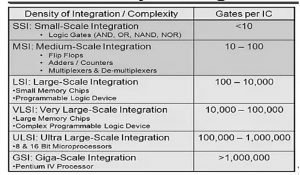
1. What is the range of integration can be designed using VLSI technology?
Ans: VLSI technology can incorporate ICs in a range of 2000 to 20,000.
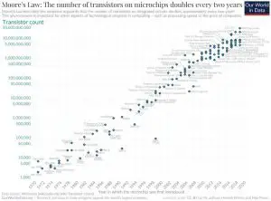
2. What is Moore’s law?
Ans: Moor’s law is one of the most significant statements that describes large-scale integration technology growth. Gordon Moor, the co-founder of Intel, predicted that the number of transistors inside an integrated cheap would be doubled every 1.5 years.
3. What is BiCMOS?
Ans: BiCMOS is one of the kinds of integrated circuits that use Bipolar Junction Transistors and CMOS to design models.
4. What is Y- Chart?
Ans: Y chart is an illustration for the representation of IC design domains. Gajski-Kuhn introduced it.
5. Name the components of FPGA architectures.
Ans: FPGA or Field programmable gate array is a specially designed integrated circuit. The interconnections are programmable to design different logics. FPGA architecture consists of –
- Logic block array (CLBs)
- Input-Output Buffers
- Programmable Interconnections
6. What is PLA and PAL? Write some differences between PAL and PLA.
Ans: PLA is acronym of Programmable Logic Array, and PAL is acronym of Programmable Array Logic. They are kinds of programmable logic devices.

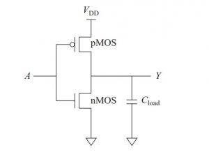
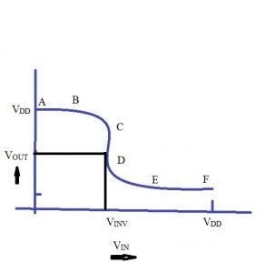
7. What is the condition for a CMOS inverter to be a symmetric CMOS inverter?
Ans: The logic voltage for a symmetric CMOS inverter will be equal to half of the supplied voltage (VDD).
VINV = VDD / 2
8. Name and explain the design rules of VLSI technology.
Ans: There are two types of design rules – Micron rules and Lambda rules.
Micron Rules: This rule deals with some of the important parameters like – min. sizes of features, permissible feature separations, etc.
Lambda Rules: The Lambda is the primary length unit.
Check this article for more!
9. What is Antenna Effect regarding VLSI technology?
Ans: While the fabrication of interconnection is under process, some of the metal lines may be partially processed. Those metal lines further gather static charges inside the clot surroundings. Later, if those lines get interconnected with transistors, the previously stored charges may start discharging during operation in progress. That discharging may affect the gate oxide. This effect is known as Antenna Effect.
10. What is PLL?
Ans: PLL is Phase Locked Loop, which can track the frequency- coming inside. PLL can also work as a clock generator.
11. What is PDN and PUN?
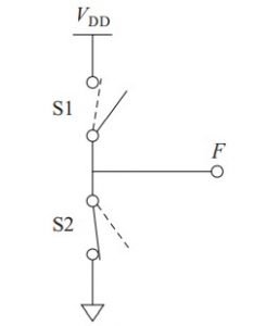
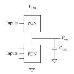
Ans: PDN is Pull Down Network, and PUN is Pull Up Network. They are used to design desired CMOS logic.
12. Which type of transistors are used in Pass Transistor Logic?
Ans: Pass transistor logic uses NMOS transistors to design models.
13. What is Domino CMOS logic?
Ans: Domino CMOS logic is implemented by connecting a static CMOS inverter at each dynamic CMOS logic’s output.
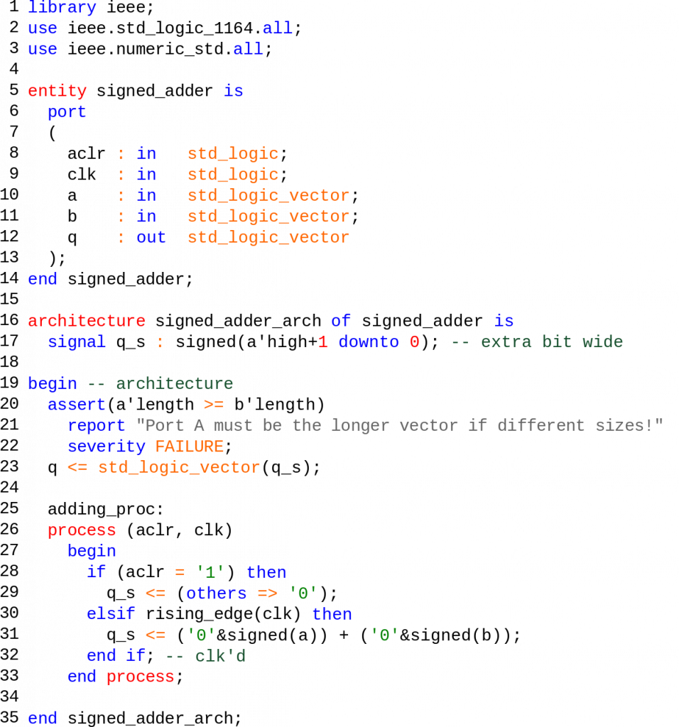
14. What is the full form of VHDL?
Ans: VHDL stands for – Very High Speed Integrated Circuit Hardware Description Language or VHSICHDL.
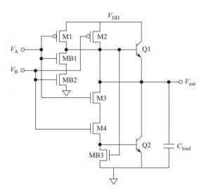
15. How many MOSFETs and BJTs are required to design a BiCMOS two-input NAND gate? Draw the circuit diagram of a two-input BiCMOS NAND gate.
Ans: To build a BiCMOS two-input NAND gate, we need 7 MOSFETs and 2 BJTs.
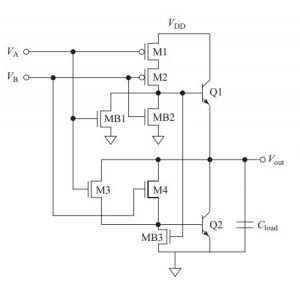
16. How many MOSFETs and BJTs are required to design a BiCMOS two-input NOR gate? Draw the circuit diagram of a BiCMOS NOR gate.
Ans: To build a BiCMOS two-input NOR gate, we need 7 MOSFETs and 2 BJTs.
17. What is ROBDD and OBDD?
Ans: OBDD is an Ordered Binary Decision Diagram, and ROBDD is Reduced Ordered Decision Diagram. These are Boolean space methodology for handling a large number of input signals.
18. Give some examples of Logic Synthesis Techniques of VLSI design.
Ans: Some of the logic synthesis techniques are – Instantiation, Macro expansion/ substitution, Inference, logic optimization, and structural reorganization.
19. What do you mean by Local-skew, Global Skew?
Ans:
Local Skew: Local skew is the change of clock to reach the launching flip-flop to reach the destination flip-flop.
Global Skew: Global skew is the alteration of first reaching flip-flop to the last reaching flip-flop.
20. What is FSM or Finite State Machines? Discuss the types of FSM.
Ans: FSM or Finite State Machines are devices consists of both combinational and sequential logic circuits. Input signals and current states help the machine to change its state.
The two kinds of Machines are –
- Moore Machine: The FSM whose outcome is contingent upon the present state of the machine.
- Mealy Machine: The FSM whose outcome is contingent upon the present state of the machine as well as upon the input signals.
21. What is HBM or Human body model regards to VLSI?
Ans: HBM or Human Body Module is a corresponding course to describe the electrostatic discharge models when the IC is in direct contact with the human figure.
22. What is Soft Error? What is SER?
Ans: Soft error occurs due to the striking of charged particles against the semiconductor devices. It can be described as a type of noise r glitch.
SER or Soft Error Rate is the prediction rate of a device to face a soft error.
23. Compare between FPGA and ASIC.
Ans: The comparative study between FPGA and ASIC is given in the below table.
| Subject of Comparison | FPGA | ASIC |
| NAME | Field Programmable Gate Array | Application Specific Integrated Circuit |
| Application | The user designs the program on his own | The user gives the description of the need; the vendor provides the required model. |
| Production Set-up Costs | Minimal production set up cost. | Relatively costlier |
| Turnaround Time | Faster Turnaround Time | Slower turnaround time |
| Capability | Lower Capability | Higher capability and efficiency for a higher volume of production. |
24. What are the modes of SFF or Scan Flip Flop?
Ans: SFF or scan flip-flop has two types of operation modes. In the general model, the flip-flop function as conventional flip-flops. In the next mode or the scan mode, the flip-flops are connected so that they will work as a series of registers.
24. What is AD HOC testing?
Ans: AD HOC testing is a strategy or process to condense the number of trials from a huge set of test outlines. It is most useful for small models where ATPG, BIST are not available.
25. What is BIST?
Ans: BIST is a Built-in self-test. It is a testing logic circuit that is placed inside a chip. BIST consists of – PRSG or pseudo-random sequence generator and signature analyser.
26. Describe Slew Balancing.
Ans: Slew is a basic term related to the rise and fallen time of the input and output waveforms. Rise time is known as rising slew, whereas fall time is known as fall slew. Slew balancing is the process of making the rise slew and fall slew equal. To do so, the corresponding resistances of the transistors are kept equal.
27. Why CMOS is preferred over BJT in VLSI designs?
Ans: CMOS technology is preferred over BJTs for VLSI designs. Some of the reasons are –
- CMOS has lower power indulgence.
- CMOS uses lower area
- Scaling of CMOS is easier than that of BJTs.
- CMOS has a lower fabrication cost.
28. State some of the DSM issues.
Ans: Some of the DSM or deep sub-micron issues are – interconnect RC delays, IR drop, induction effects, antenna effects, capacitive and inductive coupling, etc.
29. What is the package of VLSI design?
Ans: Package: It is basically the storage of various datas. VHDL packages typically made up of Declaration and Body of the packages.
30. What are the future technologies of VLSI?
Ans: Future technologies of VLSI are – ULSI (Ultra Large Scale Integration) and GSI (Giga- Scale Integration). ULSI has a range of – 100,000 gates to 1,000,000 gates per IC, and GSI has a range greater than 1,000,000 gates per IC.
For more Electronics related article click here


