Sequential Logic: 17 Important Facts You Should Know

Sequential Circuits 300x177 1

Content: Sequential Logic

Sequential logic definition:

A type of logic in which the previous sequence state of inputs as well as current input can affect the present output state.

What is sequential logic circuit?

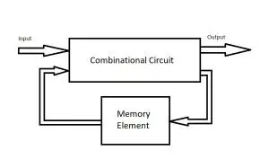
The sequential logic circuit is a combined form of the combinational circuit with a basic memory element. With the presence of a memory element, the circuit can store previous input and output states. At the same time, the sequential logic circuit is generally known as a two-state or bistable device because it has only two stable states, ‘0’ and ‘1’, one state at a time. The memory element in the circuit can store one bit at a time.

This type of circuit has a finite number of inputs with a finite number of outputs. Due to the memory element, this circuit provides the solution to our many problems. A sequential logic circuit is mainly used as a register, counter, analog to digital converter (ADC), etc.

Sequential Logic Diagram | Sequential Logic Architecture :
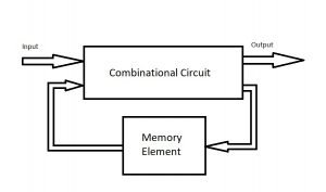
Sequential Logic Circuit
Fig.  Sequential Logic Circuit

Types of sequential logic circuits:

Generally, we can differentiate the sequential logic circuit into two basic types:

  • A. Asynchronous sequential logic circuit.
  • B. Synchronous sequential logic circuit.

Synchronous sequential logic circuits:

The output of this logic circuit depends upon the input pulse and the clock pulse of the circuit. The circuit is synchronized with the clock, i. e. the output can change only after a finite interval of time. Here memory element and the clock is a necessity. Without any clock pulse, there will be no change in output. For a change in one state output to another, this circuit waits for the next change in clock pulse.

This type of circuit may be used to synchronize all the elements present in the circuit, practically for responding to a change in input. There is a need for a finite amount of time for the processed output to occur mainly, known as propagation delay. The propagation delay can vary from element to element. So for a properly working circuit, we need a definite time interval so that all elements can get their time to respond properly. Example of the synchronous logic circuits is flip-flops, synchronous counter, etc.

Asynchronous Sequential logic circuits:

The output of this logic circuit only depends on the input pulse and the sequence of previous input data, This circuit doesn’t have any clock and doesn’t need any synchronization, so the circuit is independent of the clock, which makes it faster than the synchronous sequential logic circuit because the output can change concerning change in input with minimum time required can be affected regardless of time. The only hindrance to the speed of this circuit is the propagation delay of the circuit elements. It consumes less power, low electromagnetic interference.

Asynchronous sequential logic circuits usually perform operations in following cases :

 These circuits are mainly used when the speed of operation is a priority, such as in microprocessors, digital signal processing, for internet access, etc. Because of the asynchronous behaviour, the output sometimes may be uncertain, limting the application of the asynchronous sequential logic circuit. Forming this type of circuit is also difficult.

Difference between synchronous and asynchronous sequential logic circuits:

Synchronous sequential logic circuitAsynchronous Sequential logic circuit
The output of this logic circuit depends upon the input pulse as well as the clock pulse of the circuit.The output of this logic circuit only depends on the input pulse and the sequence of previous input data.
The clock is present in this circuit.No clock is present in the circuit.
The circuit is simple for designing.The design of this circuit is complex.
Relatively slower than that of an asynchronous sequential logic circuit.Relatively faster working than that of the synchronous sequential logic circuit.
State output is always predictableState output sometimes unpredictable
This circuit consumes somewhat high power.It consumes relatively more minor  power.

Sequential Logic State diagrams:

Sequence logic state diagram is a characteristic diagram of the circuit, in which we can determine the transition between the states concerning the input. In this type of diagram that state is mainly represented as a circle and the change from one state to another is denoted by an arrow, along with that arrow the input pulse is represented, which causing the transition between the state. When there is pulse output the arrow can be represented with the output related to the input pulse. Here the arrow starts with one circle and goes to another circle and sometimes it can come back to the same circle depending upon the condition.

Sequential logic circuit design | Sequential logic design principles

We already know that a sequential logic circuit combines the combinational circuit with a memory element. And for the memory element, we need a static memory element to store data in circuitry. So for creating a static memory cell in the circuit, we use inverters.

Steps of Sequential logic circuit design:

  1.  Create a state diagram for the required sequential circuit with the desired output states.
  2. Convert the state diagram into a state table.
  3. Chose the flip-flop as your requirement and which is satisfying all the needed conditions, use the characteristic table or excitation table for selection of the flip flop.
  4. Minimize the input functions to the flip flop with the help of a K- map or required Boolean algorithms.
  5. Use the simplified function to design the sequential circuit and if the combinational circuit is needed for the required output add it accordingly.
  6. Finally, check for the required output through the circuit.

By following the above step we can design any sequential circuit required.

Sequential MOS logic circuits:

As we know that a sequential logic circuit is a combination of the combinational circuit with a memory element. And for the memory element, we need a static memory element so that it can store data, in circuitry. So for creating a static memory cell in circuitry we use inverters.
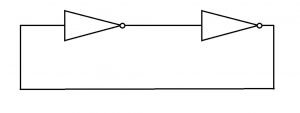
inverter
Fig.  In this figure, two inverters are connected in feedback to each other.

A static memory cell can be created by two or any even number of inverters connected in series with feedback. It has two stable states, but one stable state at a time, and the stable output state is concerning the input. When a noise (as a voltage or other form) adds up to the output, which can make the circuitry unstable, and the output may not be stable at a definite state, but as the noise crosses through either of the inverters, it gets eliminated as this circuit is regenerating always trying to return to a definite stable state, which helps us to create an active and regenerative memory cell.
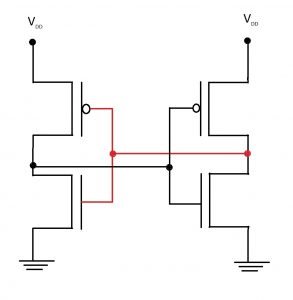
Circutits
Fig. In this figure a CMOS circuit of the two inverters connected in feedback.

The above diagram is the CMOS circuit is of the memory cell (two inverters connected in the feedback). Where this circuit will be stable at ‘0’ or ‘1’ considering the input supplied (voltage) through the input, this memory cell in CMOS is a static memory cell. And by combining the CMOS circuit of this memory cell with the combinational CMOS circuit, we can design the sequential circuit CMOS circuit.

Combinational logic vs Sequential Logic:

Combinational LogicSequential Logic
It is a type of digital logic that is composed of numerous Boolean circuits, and its output only depends on current inputs.It is also a type of digital logic composed of a combinational as well as a memory element, its output not only dependent on the current input but can also be manipulated by the sequence of previous inputs.
Its circuit is relatively costly.Its circuit is relatively cheap.
The clock is not there in its circuitry.The clock is a necessary element in the synchronous sequential circuit.
There is no memory element in its circuitry.There must be a memory element in the circuitry of this logic.
There is no feedback circuitry is present.For manipulation through past inputs, feedback circuitry is needed.
Designing the circuit through logic gates is easy.Here we can face complications in designing the circuitry due to the requirement of memory elements and feedback.
Processing of results is comparatively faster.After considering every aspect, the output processing can be relatively slower.
We can define the input-output relationship through the truth table.The input-output relationship can be defined through a characteristic table, excitation table, and state diagrams.
The requirement of this logic is mainly to perform Boolean operationsRequirement of this logic for storing data, creating counter, registers, etc.

Sequential logic circuits Applications:

With the finite number of inputs and outputs, the sequential logic circuit is used to construct a finite state machine. It can act as a register, counter, etc. With the help of a combinational circuit, many basic devices can be created like RAM (Random Access Memory), as sequential logic circuit provides us with the facility to store data it opens the door to the microprocessor and Arithmetic logic Circuit.

Sequential Logic Devices:

The output of a sequential logic device can be manipulated by the current input and by the previous input or clock pulses. Sequential devices store the last data with a memory element. With this capability of storing data these devices, open new ways to solve a problem.

Sequential devices are like counter, register, etc.

Sequential Logic chips
Sequential logic chip 3
image credit : Konstantin Lanzet, KL CHIPS F8680 SoCCC BY-SA 3.0

Advantages and disadvantages of sequential logic:

Advantages of sequential logic:

A significant advantage of sequential logic is that its circuit contains a memory element that enables storing data and creating a register, counter, and microprocessors. With the use of clock pulse, it can synchronize all the circuitry elements regardless of different propagation delays and provide proper output.  Output can be manipulated through current input, past sequence of inputs, and through clock pulse also.

Disadvantages of sequential logic:

Presence of a clock and feedback in the circuitry, the processing of the output can be slower. Complications of the circuit may increase, which can cause difficulty in building the circuitry. The output is sometimes can be uncertain.

Sequential logic history :

Sequential logic is utilized for the development of finite state machine, which is a basic building block of all digital circuitry. For more information click here.

Sequential logic circuits questions and answers | solved problems on sequential logic circuits | FAQ

Q.  How does computer ram use sequential logic ?

Q. Is ROM/RAM a combinational or sequential circuit?

Answer: – ROM (Read Only Memory) consists of Encoder, Decoder, Multiplexer, Adder Circuitry, Subtractor Circuitry, etc. The encoder is a combinational circuit that mainly converts one form of data to another format, such as decimal data to binary data. The decoder here is also a combinational circuit. The same goes for Multiplexer, Adder, and Subtractor. All are here is a combinational circuit.

 In ROM, we cannot alter the content of the memory. Therefore the output of the ROM is only dependent on the input. So there is no requirement of the past value of input or output. So, ROM has only a combinational circuit in its circuitry.

 Whereas for RAM (Random Access Memory), PROM (Programmable read-only memory), EPROM (Erasable Programmable read-only memory), EEPROM (Electrically Erasable programmable read-only memory) has a memory that can alter. In the case of PROM, it can be programmed once after manufactured. RAM, EPROM, EEPROM, where can change the state.  In this type of memory, we always need the sequential circuit for proper operation, as here, there is a need for past input and output values. The current output can be altered with the previous sequence of data. Therefore this type of memory needs a sequential circuit.

Q. Is ripple carry adder an example of sequential circuit Why?

  Answer: – A ripple carry adder is a digital circuitry which performs addition arithmetic of two different binary number. It can be designed with the cascading of a full adder connecter to the carry output, where the carry output of a full adder is connected to the input of the next full adder. As we see here, one full adder is connected to the next adder as feedback, here the output of one full adder can manipulate the output of another full adder. So here we see that past output can manipulate the present output of the circuit. Therefore ripple carry adder can be considered a sequential circuit.

Q. Why are non blocking assignments used in sequential circuits in Verilog ?

 Answer: – In non-blocking assignments when the first-time step takes place, the evaluation of the right-hand side expression of the non-blocking statement takes place after that revision of the left-hand side of the non-blocking statement takes place, and at the end of the time step, the evaluation of left-hand statement takes place.

 As non-blocking assignments do not block the evaluation of any sequential statements, the execution of these assignments simultaneously or parallelly occurs. So, for creating a sequential logic circuit in Verilog we always have to consider clocked block and non-blocking assignments. With the help of non-blocking assignments, we can eliminate the race around condition in the sequential circuitry.

Q. Define asynchronous sequential logic circuits ?

Answer : explained in asynchronous sequential logic circuits section.

Q. How many flip flops are required to build a sequential circuit which has 20 states.

Answer: – Flip Flops is a basic memory element in the sequential digital circuit, which has two stable states, and those two states can be represented as ’0’ and ‘1’, but It can store a single bit at a time.

 According to binary encoding, n number of flip flops can represent maximum 2n

Here we need 20 states of a sequential circuit

So   2n = 20

After solving the above equation, we get n = 4.322

As for,  24 there are only 16 states, but we need 20 states. Here we are 4 more states for working so we have to choose a number higher than 4. So, we will be using n=5 where  25 has 32 states, which is sufficient enough for 20 states.

Whereas in one-hot encoding there the number of flip flops required for n states is n. so there we need 20 flip flops for 20 states.

Q. How can a sequential chip be made from combinational chips alone

Answer: – When a combinational logic circuit is connected with a feedback path, the resulting circuit is a sequential logic circuit.

If we go to the diagram of essential memory elements like a flip flop, latches, we can see that the flip-flop can be created with the help of AND gate, NAND gate, NOR gate, etc., when they are connected with feedback to each other.
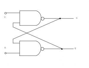
SR FF
Fig. This is a Diagram of the S-R flip flop. 

 The diagram shows two NAND gates connected with a feedback path that forms the S-R flip flop circuit. In this way, a combinational circuit can be converted into a sequential circuit.

Q. Working principle of astable sequential logic circuits

Answer:-  An astable sequential logic circuit does not have any stable state as output i.e it is not stable in any state. The output continuously transits from one state to another. This type of circuit can be used as an oscillator, such oscillator for generating clock pulse in a circuit. An example of an astable circuit is a ring oscillator.

For more articles click here
What is PIN Photodiode ? | It’s 5+ Important use and characteristics

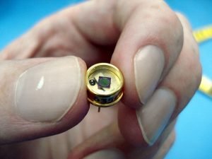
photod 300x225 1

Topic of Discussion : PIN Photodiode

What is PIN Photodiode ?

A Photodiode is a PN junction diode that operates in reverse bias. As the name suggests, PIN photodiode is a particular type of photodiode in which an intrinsic layer is placed in between a heavily doped p-type and a heavily doped n-type layer. As resistivity decreases with an increase in impurity and vice-versa, p and n layers have very low resistivity , while resistivity in the I layer is very high. PIN-Photodiode has a large depletion region which is used in the reception of light.

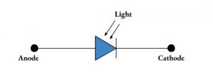
PIN Photodiode Symbol

PIN Photodiode symbol

Symbolic representation of the PIN-photodiode is the same as that of the standard p-n junction diode except for the downward arrows over the diode , which indicate light.

PIN Photodiode Structure

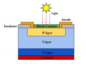
Structure of PIN Photodiode

PIN-Photodiode comprises three layers- p-layer, I or intrinsic layer , and n-layer. P-layer is doped with a trivalent impurity , and N-layer is doped with a pentavalent impurity. The I-layer is undoped or very lightly doped. P terminal acts like anode , and N terminal acts like cathode. Unlike the general PN junction diode, the width of the intrinsic layer in the PIN-Photodiode is larger.

It can be constructed in two ways:

  • Planar Structure: In this type of structure, a thin epitaxial film is fabricated on p-layer.
  • Mesa Structure: In this type of structure, already doped semiconductor layers are grown on the intrinsic layer.

PIN Photodiode Circuit Diagram

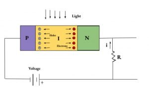
Circuit diagram of PIN Photodiode

The PIN-photodiode works as a photodetector only when it is functioning in reverse bias. The Anode is connected with the negative terminal of the battery. The positive side of the battery is connected to the cathode through a resistor.

Operation of pin photodiode | Working principle of PIN Photodiode

  • When reverse bias is applied to the device, the depletion region starts expanding in the intrinsic layer. The width goes on increasing until it reaches the thickness of the I layer.
  • As a result, the depletion region becomes free of any mobile charge carriers. So no current flows. At this point, no electron-hole recombination takes place in the depletion region.
  • When the light of sufficient energy ( h? ≥ bandgap energy of the semiconductor) enters the I region, each photon absorbed generates one electron-hole pair. These pairs experience a strong force due to the barrier electric field present in the depletion region. This force separates the pairs , and charge carriers move in opposite directions , and current is generated. Thus optical energy gets converted into electrical energy.
  • As the current is generated from the light energy, it is called photocurrent and written as Ip.

PIN Photodiode Characteristics

  • Resistivity: It offers low resistivity in P , and N layers ( less than 1kΩ/cm) and high resistivity in I layer ( up to 100 kΩ/cm)
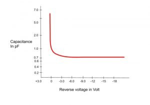
  • Capacitance: As capacitance is inversely proportional with the gap between P and N layers, capacitance in this photodiode is lower than the standard diode.    

CodeCogsEqn 39 convert.io

Where ?0= dielectric value of free space

             ?r= dielectric constant of the semiconductor

             A= area of the intrinsic layer

             d= width of depletion region

  • Breakdown Voltage: The intrinsic layer widens the depletion region , due to which breakdown voltage is very high.
  • The flow of current: The current flow is directly proportional to the amount of light incident on the detector.
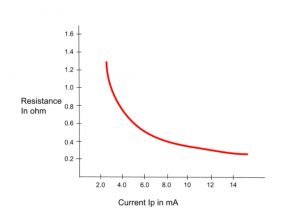
  • Forward bias condition: If it is operated in forward bias mode, the width of depletion layer reduces and current flows. In this case, the diode behaves like a variable resistor.
  • Quantum efficiency(?): It is referred to the number of electron-hole pairs generated per photon having energy h?
  • Responsivity: It measures the output gain per input (photon).

Modes of operation in PIN Photodiode

It has primarily two modes of operation-

  • Unbiased Photovoltaic Mode 
  • Reverse Biased Photoconductive Mode 

PIN Photodiode IV curves

graph1
graph 2

Photodiode pin diagram

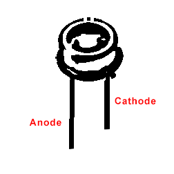
Pin configuration

Photodiode pin configuration

               Name of the pin              Identification
                  Cathode             Shorter in length
                   Anode              Longer in length

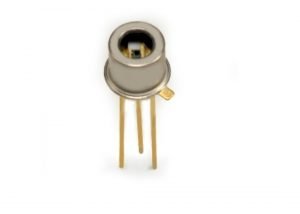
3 pin photodiode

3-pin-photodiode
Si PIN photodiode
image credit : HAMAMATSU Instruments

Three-pin photodiodes are high-speed Silicon PIN-photodiodes especially designed to detect nearby infrared light. At low bias, these devices provide the facility of wideband characteristics,  which makes them usable for optical communication and other photometry.

Noise in PIN Photodiode

Noise refers to any undesirable occurrence or an error in the received information signal. It is the amalgamation of disturbing energies coming from different sources.

Following are the noises that attribute to the total noise of a photodiode:

  • Quantum or shot noise
  • Dark current noise
  • Thermal noise

While the first two types of noises are generated from the statistical nature of photon to electron conversion procedure, thermal noise is associated with the amplifier circuitry.

Quantum or shot noise: 

It happens due to the proton to the electron conversion process. The Poisson process is followed here.  Mean square value of Shot noise iq on photocurrent ip is,

CodeCogsEqn 40 convert.io

Where, q= charge of an electron

             B= bandwidth

Dark current noise:

Dark current is the current that flows through the circuit when no light is incident on the photodetector. It has two major components- bulk dark current noise and surface leakage current noise. Bulk dark current is the result of thermally generated holes and electrons in the PN junction.

Mean square value of bulk dark current noise idb on dark current id is,

CodeCogsEqn 41 convert.io

Mean square value of surface leakage current noise ids on surface leakage current iL is,

CodeCogsEqn 42 convert.io

Thermal Noise:

It is also called Johnson noise. The thermal noise of the load resistor is much higher than the thermal noise of the amplifier as load resistance has a smaller value than amplifier resistance.

Therefore, mean square value of thermal noise ir due to the load resistance RL

CodeCogsEqn 43 convert.io

 Where KB= Boltzmann constant

             T= absolute temperature

             B= bandwidth

InGaAs PIN Photodiode

InGaAs( indium gallium arsenide) is an alloy of indium arsenide and gallium arsenide. Gallium arsenide can efficiently convert electricity into coherent light.

InGaAs PIN-Photodiode or photodetectors are optoelectronic devices capable of providing very high quantum efficiency that can range from 800 to 1700 nm. They exhibit low capacitance in extended bandwidth, high linearity, high sensitivity due to increased resistance, low dark current, and uniformity across the detector’s active area. All of these characteristics help to increase flexibility and offer a wide range of applications.

GaAs PIN Photodiode

GaAs( Gallium arsenide) is a semiconductor that has high electron mobility and high electron velocity than silicon. It can function at very high frequencies.

GaAs PIN photodiodes are used in detecting optical signals at 850 nm. It has a large activation area that ensures a stable and sensitive response. This can also be used in optical telecommunications as optical receivers, in testing machines, etc. GaAs photodiodes provide fast response, low dark current, and high reliability.

PIN Photodiode detector

The photodetector is used to convert light signal to electrical signal, their amplification, and further processing. In optical fiber systems, the photodetector is an essential element. Semiconductor photodiodes are amongst the most widely used detectors as they offer excellent performance, are small in size, and low in cost.

Example:  Gallium arsenide photodiode, Indium gallium arsenide photodiode, etc

PIN Photodiode in optical communication

 Photodetectors are vividly used in the automobile sector, medical purpose, Safety equipment, cameras, industry, astronomy, and most importantly, in communications. There are two distinct photoelectric mechanisms available for photodetection:

  1. External effect: PMT or photomultiplier tubes
  2. Internal effect: PN junction photodiodes, PIN-photodiodes, avalanche photodiodes         

Photodetection principle:       

  • Electron-hole pair photogeneration occurs
  • The PIN junction is reverse biased
  • The depletion region sees carrier drift
  • Electron-hole pair moves in the opposite direction and causes photocurrent

PIN Photodiode radiation detector | PIN photodiode gamma detector

PIN photodiodes are able to detect individual photons in gamma radiation. A PIN photodiode, a comparator, and four low noise operational amplifiers are together used in this process.  

 In reverse bias condition, when photons strike the depletion region, they produce a small charge directly proportional to the energy of photons. The resultant signal gets amplified and filtered by the op-amps. Comparator distinguishes the signal and the noise. The final output of the comparator shows a high pulse every time a gamma photon with minimum required energy strikes the PIN photodiode.

PIN Photodiode receiver

Optical receivers are responsible for the optical to electrical energy conversion. The most crucial element of the optical receiver is the photodiode.

The receiver must detect distorted, weak signals first and then, based on the amplified version of that signal, decide which type of data was sent. Errors coming from various sources can be found associated with the signal. So signals should be controlled , and processed with utmost precision as noise consideration is a significant factor in the design of the receiver.

Silicon PIN Photodiode

Silicon or Si PIN-photodiodes can accommodate different applications. Due to the PIN structure, it produces fast response and high quantum frequency to detect photons. They are capable of light detection in the range of 250 nm to 1.1 μm. It detects high-energy radiation in high frequencies. The width of the depletion region varies from 0.5 to 0.7 mm.

Si PIN photodiode detector

In PIN photodiodes, the depletion region almost coincides with the intrinsic layer. Charge carrier generation happens due to the incident radiation.

 Along with the light radiation, Gamma radiation, X radiation, particles too can generate charge carriers.

When photons meet with the metal contact of the diode, it produces electron-hole pairs in large numbers. Electrodes collect these , and the signal is generated. Electron-hole pairs that are more mobile helps in receiving easily detectable signals. Those are subsequently processed through a low noise amplifier , and the analyzer detects the amount of radiation from the pulses.

PIN photodiode array

Photodiode arrays are generally used in X-ray machines by scanning the object in the image line by line. X-rays are transformed into light through the scintillator crystal. Then the photodiode measures light intensity.

High-speed PIN Photodiode

High-speed PIN-Photodiodes are preferred for their precise triggering against signal strength, enhanced sensitivity, low operating voltage, and high bandwidth.

PIN Photodiode Amplifier

Operational amplifiers are used with a feedback resistor to convert photocurrent to measurable voltage. It is also called a trans-impedance amplifier.

Application of pin photodiode

PIN-photodiodes are one of the most popular photodiodes that have varied characteristics , making them suitable for different applications. Besides photo-detection, it is used in DVD players, CD drives, switches, medical treatment, and many more.

  • ‌High voltage rectifier: The intrinsic layer provides a greater separation between the P and N region, allowing higher reverse voltages to be tolerated.
  • RF and DC-controlled microwave switches: The intrinsic layer increases the distance between the P and N layers. It also decreases the capacitance , thereby increasing the isolation in reverse biased condition.
  • Photodetector and photovoltaic cells: Light to current conversation occurs in the depletion region. As the width of the intrinsic layer is more, it improves the performance of capturing light.
  • RF and variable attenuators
  • ‌RF modulator circuit
  • ‌MRI machine

PIN Photodiode Advantages and Disadvantages

PIN photodiode Advantages

  • ‌It has high light sensitivity.
  • ‌The response speed is high.
  • ‌Its bandwidth is wide.
  • ‌Implementation cost is low.
  • ‌It generates low noise.
  • ‌Temperature sensitivity is low.
  • ‌It is small in size.
  • ‌Longevity better than standard diodes.

PIN photodiode Disadvantages

  • ‌It can only be operated in the reverse biased condition.
  • ‌The voltage applied must be low.
  • ‌It is sensitive to every kind of light.
  • ‌Temperature specifications have to be maintained.

FAQs

What is the use of polar capacitance in PIN photodetector?

Polar capacitance means the capacitor plates are electrodes having a positive and a negative polarity. In a PIN photodetector, the P and N layers act as electrodes, and as the width of the depletion layer is vast; the capacitance value is low. Due to low capacitance, the speed improves.

What is the advantage of PIN photodiode?

It has high sensitivity, low noise, wide bandwidth, low implementation cost. the detailed explanation is in top section .

What does I in PIN Photodiode stands for?

I in PIN photodiode stands for Intrinsic layer.

What is the difference between a regular photodiode and a PIN photodiode?

The increased intrinsic layer makes PIN photodiodes capable of carrying more current and also improves frequency response. The detailed explanation is in top section .

What are the drawbacks of PIN photodiode?

It is highly light-sensitive , and it can perform well only in reverse bias.

What is photodiode and its symbol?

A photodiode is a semiconductor that converts light energy in electrical energy.

Symbol

What is a photodiode array?

It is a sensor used in photodetection, spectrophotometry , etc.

What is photodiode most commonly used?

The PIN-photodiode is the most commonly used photodiode.

For more article click here

Op Amp: 7 Important Parameters

1280px Op amp symbol.svg 300x255 1

Points of Discussion

Structures, PIN outs & Schematic

Op amp diagram

The op-amp diagram marks the inputs, outputs, and saturation voltage connections. It is an open-loop system. The below image represents an op-amp diagram.

Op amp pinout

In-general typical op-amp ICs have eight pins. Seven are functional, while one pin is dedicated for output. It takes four inputs; 2 of them are for inverting terminal and non-inverting terminal, and the rest 2 are for positive and negative saturation voltage. The pinout of IC741 is given above.

Op amp schematic

The below image gives a schematic view of an op-amp.

Op amp
Schematic Diagram by: InductiveloadOp-Amp Internal, marked as public domain, more details on Wikimedia Commons

As we can see in the image, an op-amp consists of transistors and resistors. The input impedance is high because of the Darlington pair of the NPN transistors. There are two differential gain stages, and the output is taken from the single-ended emitter follower. The transistors T1 and T2 are identical, and so as the T3 and T4.


Types and Applications

Op amp applications | Op amp uses

Op-amps are one of the essential elements for circuit designing in electronics. They are used in various places. Some of the examples are –

Unity gain buffer, phase shift oscillator, current to voltage follower, the voltage to a current follower, summing amplifier, integrator, differentiator, half-wave rectifier, peak detector, etc. There are many more applications of the op-amp. Almost every electronic gadget is incorporated with an op-amp.

High pass filter op amp

A high pass filter can be built using an RC filter circuit and a typical op-amp. Combining a passive RC filter with op-amp functions like an active high pass filter. The inverting or non-inverting terminal operation of the op amp is required for the circuit. The below image represents a high pass filter op amp circuit.

Op amp bandpass filter

A bandpass filter allows a signal of the specified frequency range only. This filter filters out other components of frequencies. Op-amps are used to make such types of filters. The circuit is designed by cascading a high pass filter with an op-amp and then a low pass filter.

Subtractor op amp

Subtractor op-amp amplifies the difference between the two input voltages and provides that as output. It performs the subtraction operation, unlike a summing amplifier which adds up the input voltages. That is why it is known as subtractor op-amp.

Op amp adder

Op-amp adder or summing amplifier is the amplifier that amplifies the summation of the input voltages and provides as output. It performs summation or addition operation, unlike a differential amplifier which performs subtraction operations. The circuit diagram is given above.

Unity Gain op amp

A unity gain op-amp or a voltage follower circuit, or a buffer circuit is a specially designed non-inverting amplifier model. Observe the circuit of the non-inverting amplifier given above. If we made the feedback resistance zero and the inverting terminal infinite resistance, the amplifier’s gain would be unity. That is why this circuit is known as unity gain op-amp or unity gain buffer. This buffer is used for impedance matching.

Op amp oscillator

It is also possible to create an oscillator using an op-amp. The below-given image represents the circuit diagram of a phase shift RC oscillator.

Op amp
Oscillator, By: Jontse at English WikipediaOpAmpHystereticOscillator, marked as public domain, more details on Wikimedia Commons

After some general calculations, we have found out that oscillation frequency is f = 1/ (2πRC -/6) and the voltage gain Av = -29 for sustained oscillation.

Audio op amp

Operational amplifiers are heavily used in audio processing and audio mixers. An op-amp can amplify weak voice signals. Several types of audio op-amps are available in the market. Some of them are – LT1115, UA741, etc.

Op amp level shifter

In a single supply op-amp, the op-amp can level shift a ground-referenced signal. A level shifter can translate logic signals from one level to another. Sometimes there is a need for converting a positive to negative signal into an acceptable range for a single supply analog to digital converter.

Op amp voltage divider

Op-amps are also used as a voltage divider. Op-amp is used to make voltage dividers as using op-amp can increase the system’s gain.

Single supply op amp

Single supply op amp is such a special op-amp with only one supply terminal. The supply terminal is typically the +Vcc. So, the output lies between the range of +Vcc and the ground (GND) for an input signal.

High Voltage op amp

A high voltage amplifier is typically used to amplify the input signal to a high voltage output signal. It can provide the power gain at the voltage and current combinations. Some of the high voltage op-amps applications are – inkjet printers, ultrasound transducer, Geiger counters, biomedical tests, etc.

For Detail Circuit Analysis of Circuits… Click Here!

Various kinds of IC

45588 op amp

It is another integrated circuit that operates op-amp. It is a high-performance eight-pin IC that doesn’t need any external frequency compensator components. Some of the other models are – CF158MT, AN45588, LA6458, etc.

lm358 op amp

lm358 is another type of IC that consists of a couple of op-amps. It is a low-power IC, which National Semiconductor first developed.

ua741 op amp

This is another type of IC that includes an operational amplifier. It has eight pins. The maximum supply voltage is +18V, and the maximum differential input voltage is +15V. The CMMR is 90 dB. UA 741 is used in audio applications, music players.

Lm324 op amp

Lm324 is a specially built IC, which can function as an amplifier, comparator, rectifier, etc. This IC has 14 pins, representing four op-amps. It has a wide bandwidth of around 1 MHz and a gain of 100 dB. They are applied in various fields of robotics, oscillators, etc.

Ne5532 op amp

Another IC of the op-amp is ne5532. It is a high-performance amplifier that has excellent DC and AC voltages. It has low noise, maximum output swing bandwidth, and a high slew rate. Different variations of this type of ICs are – NE5532A, SA55332, etc.

Important Parameters, Rules, Equations

Op amp circuit analysis

The op-amp circuit analysis reveals the functionality of each part of an op-amp and how they are connected or interconnected to provide the output path. Circuit analysis of op-amp can be classified into two types –

  1. open-loop circuit analysis
  2. closed-loop circuit analysis.

The open-loop circuit analysis analyzes the system without the feedback system, and the closed-loop circuit analysis is the analysis of a circuit with a feedback system.

The concept of virtual ground, high input impedance, and infinite gain are necessary for the op-amp circuit analysis.

Op amp golden rules

One op-amp designer should always keep in mind some essential rules. They are –

  1. Op amp provides infinite gain.
  2. The input impedances are high.
  3. No current flows through the op-amp at the beginning.
  4. The offset voltage is adjusted to make it zero.

Op amp formulas

There are no hard and fast formulas for the op-amp. There are several types of op-amps, and they have their specific equations and formulas. Like – formulas for output of Non inverting op amp: V0 = [ 1 + (Rf/R1)] * Vin and formulas for output of Inverting op amp: V0 = – (Rf/R1) * Vin

Input impedance of op amp

The input impedance is high because of the Darlington pair of the NPN transistors. For an ideal op-amp, the input impedance is infinite. Due to the high input impedance, we can assume that the current flows through the feedback at the beginning stage. Typically, the values are in between 1 megaohm to 10 tera ohms.

Output impedance of an op amp

Output impedance of op-amp referrers to the impedance provided by an op-amp at the output stage. An ideal has an output impedance of 0 ohms. The output driver circuit causes the output impedance of an op-amp.

Open loop gain of op amp

Open loop gain of an op-amp is the device’s gain when there is no feedback associated with it. For an ideal op-amp, the open-loop gain is infinite. A typical open-loop gain of the typical op-amp is around 100 dB.

Op amp offset voltage

An op-amp’s offset voltage is defined as the differential DC voltage between the input terminals. For an ideal op-amp, the offset voltage is zero. But for the practical op-amp, the external voltage is given to the op-amp.

Slew rate of op amp

Slew rate of the op-amp is the rate of change of the output signal if there is a step-change in the input signal. It is a parameter for the measurement of performance. The unit of slew rate is V/ ms. For an ideal op-amp, the slew rate is zero. It means that the input change will be reflected immediately in the output. For a typical practical op-amp, the slew rate value is 10 V / μs.

Op amp bandwidth

The bandwidth of an amplifier is referred to as the range of frequency above which the gain of the amplifier is higher than 3 dB. For a 741 MHz amplifier, the closed-loop amplifier is 1 MHz.

Op amp current source

An external current source with an op-amp provides a load resistance independent current. And as we have previously grounded the circuit, there is no chance of exposing two connections.

Op amp transfer functions

It is possible to obtain transfer functions of op-amp if the op-amps are represented in a classical feedback block diagram. Using the process of superposition, the transfer function can be obtained. The transfer function for the non-inverting terminal can be written as R1 / (R1 +Rf).

Op amp saturation

There is two input terminals, which takes positive and negative saturation voltages. Now, when an op-amp is in saturation, it means that the op-amp’s output is any of the saturation voltage provided from the supply.

How does an op amp work?

An op-amp typically goes through three stages of operations. The first one – differential input stage with higher input impedance, the gain stage in the second stage, and the push-pull output stage of lower output impedance.

What does an op amp do?

An op-amp or operational amplifier is an electronics device that performs certain mathematical operations and amplifies the input signal.

Silicon Controlled Rectifier: 19 Facts You Should Know

SCR

What is SCR ?

SCR | Silicon Controlled Rectifier Definition

  • A SCR, sometimes also called Semiconductor Controlled Rectifier is a three-terminal solid state power device and is widely used for various power electronic applications. It is also sometimes called as a thyristor.
  • An Silicon Controlled Rectifier has three terminals namely anode, cathode and gate.
  • The SCR can be turned on by passing a small current through the gate terminal to the cathode, provided the anode terminal is at a higher potential than the cathode.

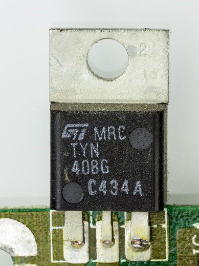
A typical Silicon Controlled Rectifier looks as follows:

Silicon Controlled Rectifier
Reference : © Raimond Spekking / CC BY-SA 4.0 (via Wikimedia Commons), Laptop Acrobat Model NBD 486C, Type DXh2 – STMicroelectronics TYN408G on Power Supply Unit-4439CC BY-SA 4.0

Silicon control rectifier symbol

An Silicon Controlled Rectifier is denoted by the following symbol for all its uses in circuit diagrams and other representation purposes.

SCR Symbol

Types of Silicon Controlled Rectifier

The thyristors are categorized as follows:

  • The Force-commutated thyristor.
  • Line-commutated thyristor.
  • The Gate-turn-off thyristor (GTO).
  • Reverse-conducting thyristor (RCT),
  • Static induction thyristor (SITH)
  • Gate-assisted turn-off thyristor (GATT)
  • Light activated silicon-controlled rectifier (LASCR).
  • MOS turn-off (MTO) thyristors emitter turn-off (ETO) thyristors,
  • Integrated gate-commutated thyristor (IGCT).
  • MOS-controlled thyristor (MCTs).

Why SCR is called silicon controlled rectifier ?

  • Generally, rectifiers can be classified as controlled rectifiers and uncontrolled rectifiers.
  • Diodes come under the category of uncontrolled rectifiers as they conduct without any control, as long as the anode voltage is greater than cathode voltage (also called forward-bias condition)
  • SCRs, on the other hand, are called controlled rectifiers as they conduct only when the gate terminal is triggered. Thus, by providing a triggering pulse to the gate, we can control the working of the thyristor, as long as it is in the forward bias condition

Thyristor vs SCR

SCRs and Thyristors are essentially the same and can be used interchangeably. In this article also, both the terms will denote the same device.

High Power Silicon Controlled Rectifier

SCRs are known for their high power-handling capability. Natural or line-commutated thyristors having rating of 6000V, 4500A are also available. On an application level, these are huge values and therein lies the importance of SCRs. SCRs can handle such huge amounts of voltages and currents without damaging itself. The characteristics of the SCRs ensures that they will always have important power electronic applications.

Operation of Silicon Controlled Rectifier

  • An SCR can be ON state by forward-biasing the anode-cathode junction and applying a pulse of positive gate current for a short duration. Once the device begins to conduct, we can remove this gate pulse and the Silicon Controlled Rectifier is latched on, though it is not possible to turn off the SCR by any gate pulse.
  • If the anode current attempts to go to -ve, on account of the circuit onto which the SCR is connected, SCR may turn-off and the current will be 0.
  • In its OFF-state, the thyristor will halts a forward polarized voltage and will not be in conducting stage.
  • The I-V characteristics of an SCR can be studied to understand these points in further detail.

It is interesting to note that an SCR can be used for both AC and DC, Once the conditions for turning on are met – forward bias voltage and positive gate pulse – it conducts all currents, regardless of whether it is AC or DC.

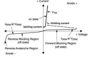
Silicon Controlled Rectifier Characteristics

  • Till the thyristor is triggered by a gate pulse, if a positive voltage is applied across the anode-cathode junction, the element is said to be in forward blocking state
  • Once the device starts to conduct, the SCR is ON and can be said to be in forward conducting state
  • If the voltage applied is negative, the device is said to be in reverse blocking region. In reverse blocking state, only a negligibly small leakage current flows in the thyristor.
  • Once the negative voltage increases beyond a value called reverse breakdown voltage, the thyristor will start conducting in the negative direction. This voltage is also called peak reverse voltage. This is also called Zener breakdown or avalanche region.

We may study the following graph of Silicon Controlled Rectifier (SCR) characteristics to get a better idea.

Latching Current

Once the gate pulse is removed, the current flowing from anode to cathode must be more than a minimum vale, called latching current, to keep the device in the ON state. Otherwise, the device goes back it the blocking state.

Holding Current

  • Small anode current is essential to keep the thyristor in the ON-state, That is known as holding current.
  • The holding current is less than the latching current.

Silicon Controlled Rectifier Applications

Due to the controllable nature of the Silicon Controlled Rectifier and their availability in very wide range of voltage and current ratings, SCRs find their use in a wide variety of applications.

Some of them are

  • Variable Speed Motor Drives
  • AC motors, lights, welding machines
  • Fault Current Limiters
  • Circuit Breakers
  • Light Dimmer Circuits
  • Electric Fan Speed Control
  • High Power Electrical Applications

Silicon Controlled Rectifier Dimmer

  • As, SCR is a controllable device, it can be used in dimming circuits.
  • The basic idea behind this process is that the point on the waveform where the device is turned on is changed. Essentially, it is also a form of phase control. It is also called forward phase dimming.
  • Generally, sinusoidal supply is given to the lights. So, as opposed to turning on at the point of zero crossing, we turn on at different instants, thereby controlling the power.
  • Some of the drawbacks of SCR Dimmer circuits are hum/noise, electrical noise(harmonics) and inefficiency.

SCR Heater Control

  • The general idea behind working of SCR Heater is same as that of in SCR Dimmer, i.e we control the power given to resistor loads by changing the instant of turn-on.
  • The SCR heater works by varying the time the electric heater is turned-on & therefore modulating the amount of heat supplied.
  • The SCR control can deliver electrical power in mainly 2 ways, phase angle fired and zero voltage switched modes.

Phase Angle Fired Mode

In this mode, the control is such that a percentage of power is turned on in each cycle (i.e one cycle of an alternating current). This can give smooth & variable power delivery to the heaters. Essentially, the time instant at which a gate pulse is given to the SCR is varied. This is what the term “phase angle” in the title corresponds to.

Zero Voltage Switched

Here, the switches turn and off full cycles of the sinusoidal waveforms proportionately so that   by varying the number of AC cycles, we can get the required power at the output.

SCR Power Controllers

  • The principle behind SCR power controllers are basically what we have discussed before; control the flow of electricity(and hence power) from the supply to the heater.
  • The find uses in industries and manufacturing processes for temperature regulation for different applications.
  • It basically adjusts the firing angle(phase angle from zero-point crossing of sine wave to the instant where gate pulse is applied) to maintain a constant voltage output, which is set.

SCR Motor Controller

  • SCRs can be employed to control the speed of a DC motor using the following electrical circuit.
  • Two SCRs are used to convert the input AC voltage into a pulsating dc voltage.
  • This pulsating dc voltage can be varied by controlling the output of the SCR rectifier circuit, which in turn is controlled by the timing of firing of gate pulses. Essentially, output voltage is varied.
  • In this way, SCR can operate at different levels & apply various voltages to the motor armature, thereby controlling the speed of the DC motor. If the thyristor conductors for shorter durations, its output voltage(of the rectifier circuit) becomes lower, lower voltage is applied to the DC motor and therefore the speed of the DC motor is reduced.

SCR vs TRIAC

  • The main difference between an SCR and a TRIAC is that SCR is a unidirectional device, which means it allows current flow in only one direction, whereas a TRIAC is a bidirectional device i.e it allows current flow in both the directions.
  • For triggering an SCR, a positive gate pulse is required whereas most TRIACs can be triggered by applying either a negative or a positive voltage to the gate terminal.
  • TRIACs are mainly used to control AC power

3 Phase SCR

  • Three-phase SCRs are circuits in which SCRs are used in each phase leg i.e for the 3 phases. The functioning and application of the SCRs are same as before, with only difference being that they are used for 3-phase supplies now.
  • As before, SCRs are used in two control modes, zero-crossing mode and phase angle control mode. Their working is same as that explained before

Frequently Asked Questions

Q. In an SCR silicon controlled rectifier why is the holding current less than the latching current ?

  • Latching current, as defined before, is the minimum current that must be present at the point of gate pulse removal to maintain conduction, whereas Holding Current is the minimum current that is required to be maintained to keep the device in the ON state.
  • The latching current limit is purposely kept greater than holding current so as to avoid misfiring of SCRs and provide smooth operation.

Q. How an SCR is triggered ?

Operation of Silicon Controlled Rectifier

Q. Why SCR is called a controlled rectifier ?

An SCR is called a controlled rectifier because as opposed to a diode, the turn-on time can be controlled for the device. Hence, the voltages at the out of the Silicon Controlled Rectifier are controllable depending on the instant of turn-on.

Q. What is SCR and its types?

Types of Silicon Controlled Rectifier

For more details on SCR, click here

For more articles, click here

Magnetron Microwave: 5 Complete Quick Facts

Magnetron2 300x204 1

Points of Discussion: Magnetron Microwave

Introduction to Magnetic Microwave | What is Magnetron?

A magnetron is a kind of Microwave Tube. Before discussing magnetron and its related topics, let us find out some of the basic definitions.

Microwave Tubes: Microwave tubes are devices which generate microwaves. They are the electron guns which produces linear beam tubes.

Now, the definition of Magnetron is given as –

Magnetron: Magnetron is a type of vacuum tube which generates signals of the microwave frequency range, with the help of interactions of a magnetic field and electron beams.

Magnetron tube consumes high-power, and its frequency depends on the physical dimension of the tubes’ cavities. There is a primary difference between a Magnetron and other types of Microwave Tubes. A magnetron works only as an Oscillator but not an amplifier, but a Klystron (a Microwave Tube) can work as an amplifier and as an Oscillator.

Magnetron Microwave
A typical Magnetron Microwave, Image Credit: HCRS Home Labor Page, Magnetron1CC BY-SA 2.0 AT

A Brief History of Magnetron Microwave

The Siemens Corporation developed the very first magnetron in the year 1910 with the guidance from scientist Hans Gerdien. Swiss physicist Heinrich Greinacher finds out the idea of electrons’ motion in the crossed electric and magnetic field from his own failed experiments of calculation of the mass of electrons. He developed the mathematical model around the year 1912.

In the United States, Albert Hull started working to control electrons’ motions using a magnetic field rather than using the conventional electrostatic field. The experiment was initiated to bypass the patent of ‘triode’ of Western’s Electric.

Hull developed a device almost like a Magnetron, but it had no intention to generate signals of microwave frequencies. Czech physicist August Žáček and German physicist Erich Habann independently discovered that Magnetron could generate signals having frequencies of Microwave range.

The invention and increased popularity of RADAR increased the demand for devices which can produce microwave at shorter wavelengths.

In the year 1940, Sir John Randall and Harry Boot of University of Birmingham developed a working prototype of a cavity magnetron. In the beginning, the device produced around 400 Watts of power. Further development like water cooling and several other improvements hiked the produced power from 400 W to 1 kW and then up to 25 kW.

There was a problem related to the frequency instability in the magnetron developed by British scientists. In 1941, James Sayers solved that problem.

Magnetron Microwave
The cavity magnetron developed by Sir John Randall and Harry Boot of University of Birmingham, Magnetron Microwave, Image Credit: Elektrik FanneR&B MagnetronCC BY-SA 4.0

Applications of Magnetron

A magnetron is a beneficial device, has several applications in various fields. Let us discuss some of them.

  • Magnetrons in Radar: The use of Magnetron for a Radar used to generate short pulses of high-power Microwave frequencies. A magnetron’s waveguide is attached with any of the antennae inside a Radar.
    • There are several factors of Magnetron which causes complexity to the Radar. One of them is the problem related to the frequency instability. This factor generates the problem of frequency shifts.
    • The second characteristics are that a magnetron produces signals with the power of broader bandwidth. So, the receiver should have a broader bandwidth to accept them. Now, having a wider bandwidth, the receiver also receives some sort of noise which is not desired.
Magnetron Microwave
An early commercial radar for airport, Magnetron Microwave, Image by: Unknown authorUnknown author, Magnetron radar assembly 1947, marked as public domain, more details on Wikimedia Commons
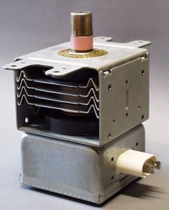
  • Magnetron Heating | Magnetron Microwave Ovens: Magnetrons are used to generate microwaves that are further used for heating. Inside a microwave oven, at first, the magnetron produces the microwave signals. Then, the waveguide transmits the signals to an RF transparent port into the food chamber. The chamber is of a fixed dimension, and also close to the magnetron.  That is why standing wave patterns are randomized by the revolving motor, which rotates the food inside the chamber.
Magnetron Microwave
Microwave Oven, Magnetron Microwave applications, Image Credit: The original uploader was 吉恩 at Chinese Wikipedia., WeiboluCC BY-SA 3.0
  • Magnetron Lighting: There are plenty of devices available which lights up using the Magnetron excitation. Devices like the sulfur lamp is a prime example of such light. Inside the devices, magnetron generates the microwave field, which is carried out by a waveguide. Then the signal is passed through the light-emitting cavity. These types of devices are complex. Nowadays, they are not used instead of more superficial elements like Gallium Nitride (GaN), or HEMTs are used.

Construction of Magnetron

In this section, we will discuss the physical construction and components of a Magnetron.

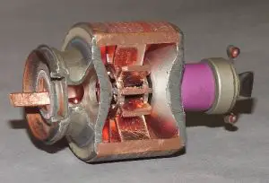
The magnetron is grouped as a diode as it is deployed on grid. The anode of the magnetron is set into a cylindrical shaped block which is made up of copper. There are filaments with filament lead and the cathode at the centre of the tube—the filaments-leads help keep the cathode and filament attached with it at the centre. The cathode is made up of high-emission material, and it is heated for the operation.

Magnetron Microwave
A Magnetron with its parts, Magnetron Microwave, Image Credit: HCRS Home Labor Page, Magnetron2CC BY-SA 2.0 AT

The tube has 8 to 20 resonant cavities which are cylindrical holes around its circumference. The internal structure is divided into several parts: the number of cavities present in the tube. The division of tube is done by the narrow slots connecting the cavities to the centre.

Each cavity functions like a parallel resonant circuit where the anode copper block’s far-wall works as an inductor. The vane tip region is considered the capacitor. Now, the resonant frequency of the circuit is dependent on the physical dimensions of the resonator circuit.  

It is evident that if a resonant cavity starts oscillation, it excites other resonant cavities and they start oscillation too. But there is one property that every cavity follows. If a cavity starts oscillation, the next cavity starts oscillation with 180 degrees delay in phase. This applies to every cavity. Now, the series of oscillation creates a slow-wave structure which is self-contained. That is why this type of Magnetron construction is also known as “Multi-Cavity Travelling Wave Magnetron”.

Magnetron Microwave
Central cathode in the middle of the magnetron microwave, Image Credit: Pingu Is SumerianMagnetron section transverse to axisCC BY-SA 3.0

The cathode supplies the electrons necessary for the energy transfer mechanism. As mentioned earlier, the cathode is in the centre of the tube, further set up by the filament leads. There is a particular open space between the cathode and anode which needs to be maintained; otherwise, it will cause malfunction to the device.

There are four types of cavity arrangement available. They are –

  • Slot-type
  • Vane-type
  • Rising Sun type
  • Hole and slot type

Operation of a Magnetron Microwave

Magnetron goes under some phases to generate signals of microwave frequency ranges. The phases are listed below.

Though the name of the phases is indicative enough to let us discuss the incidents, those occur in each phase.

Phase 1: Electron Beam generation and acceleration

The cathode inside the cavity posses the negative polarity of the voltage. The anode is kept in a radial direction from the cathode. Now, indirect heating of cathode causes the flow of electron towards the anode. At the time of generation, there is no magnetic field present in the cavity. But after the generation of the electron, a weak magnetic field bends the path of the electrons. The path of the electron gets a sharp bend if the strength of the magnetic field increases further. Now, if the velocity of the electrons gets increased, the bend becomes sharper again.

Phase 2: Velocity control and changes of Electron beam

This phase occurs inside the ac field of the cavity. The AC field is located from adjacent anode segments to the cathode region. This field accelerates the flow of the electron beam, which is flowing towards the anode segments. The electrons which flow toward the segments gets slowed down.

Phase 3: Generation of “Space Charge Wheel”

The flows of electrons in two different directions with separate velocities causes a motion known as “space charge wheel”. This helps increase the electrons’ concentration, which further delivers enough power for the radio frequency oscillations.

Phase 4: Transformation of energy

Now, after the generation of the electron beam and its acceleration, the field acquires energies. The electrons also dispense some energy to the field. While travelling from cathode electrons dispenses energy at every cavity it passes through. Loss in energy causes a decrease in speed and eventually deceleration. Now, this happens multiple times. The released energy is efficiently used, and up to 80% efficiency is reached.

Health Related Concerns from Magnetron Microwave

A magnetron microwave produces microwave signals which may cause issue to human bodies. Some magnetrons consist of thorium in their filament, which is a radioactive element and not good for humans. Elements like beryllium oxides and insulators made with ceramics are also dangerous if they are crushed and inhaled. This can affect the lungs.

There are also chances of damages from overheating of magnetron microwave ovens. Magnetrons require high voltage power supplies. So, there is a chance of electrical hazards as well.

Time Domain Reflectometer: 3 Important Facts

Megger Time Domain Reflectometer MTDR1 1

Cover By: https://giphy.com/embed/vNNkcmf2sx6TF6maey

via GIPHY

Points of Discussion

Introduction to Time Domain Reflectometer

Before we start learning about the time domain reflectometer – TDR, let us know a reflectometer.

Reflectometer: A reflectometer is a type of circuit that isolates and samples the incident and reflected powers from a load using a directional coupler.

Reflectometers are prime applications of passive microwave components. A reflectometer is used in a vector network analyzer as it can measure various parameters like – reflection coefficient for the one-port network, scattering parameters for the two-port network. It can also be used in replacement of an SWR Meter or also as a power monitor.

Time Domain Reflectometer: A time-domain reflector or TDR is an electronic device based on a reflectometer’s property that finds out characteristics of electrical lines from the reflected waves.

TDRs are used for finding out faults in cables like twisted pairs of cables or coaxial cables. This article will learn more about the device, the uses of the time-domain reflector, and explanations about it.

Time Domain Reflectometer
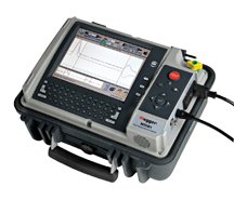
A typical Time Domain Reflectometer, Image Credit: By Megger Ltd. – Megger Ltd, CC BY 3.0, Link

Know about 7+ Applications of Microwave Engineering and Overview. Click Here!

Description of Time Domain Reflectometer

Working Principle

A TDR analyzes the reflected signals sent by itself. To analyze the reflections, it first transmits a signal along the cable and waits for the reflection. If there are some defects or mismatches in the transmission line or the cable, the part of the incident wave is reflected. TDR receives the reflected wave and then analyzes it to locate and measure the faults. But if there are no defects or everything is fine, then the signal reaches the far end without reflection, and the cable is considered acceptable. The working principle of a Time Domain Reflectometer is almost similar to the working principle of a RADR.

Analysis

The TDR analyzes the reflected wave. It is interpreted that the amplitude of the reflected wave determines the impedance of discontinuity. The reflected pulses also determine the distance of the reflected wave, which further determines the fault’s location.

Time Domain Reflectometer
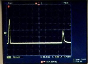
Readings from a TDR, Image Credit: Constant314TDR trace of cable with open terminationCC0 1.0

Method

Time Domain Reflectometer starts its operation by sending impulse or step signals or energies. Then it observes the reflected energy or the signals subsequently. The discontinuity of impedance is measured and analyzed by the reflected pulses of energies as the amplitude, magnitude, and waveforms help in analyzing.

For example, suppose an impulse function is sent from TDR towards a connected load. In that case, the reflectometer shows an impulse signal on its display, and the amplitude indicates the impedance of discontinuity. The following expression gives the relation between the load impedance and the magnitude of the reflected wave.

P = (RL – Z0) / (RL + Z0)

Z0 is the characteristic impedance of the transmission line or the coaxial cable. RL is the connected load resistance.

Any impedance discontinuity is observed as the termination impedance, and the termination impedance replaces it. The process consists of rapid changes in the characteristic impedance of the transmission lines.

Transmitted signals of TDRs

Time-domain reflectometers use various kinds of signals as incident signals. Some of the transmitters use pulse signals. Some of them use fast rise time step signals. Some of them also use impulse functions of signals.

TDRs using pulse signals send the pulse through the cable. Their firmness depends on the width of the pulse sent by them. That is why narrow pulse signals are preferred. But there is a shortcoming for the narrow width pulses as they are of high frequencies. High-frequency signals get distorted inside large cables.

Reflected Signals of TDR

Typically, the waves reflected from the load impedance or due to the impedance of discontinuity are similar to the incident waves in their shapes. Still, the magnitude and other properties get varied. If there is some change in the load impedance, the reflected wave does the exact change in its parameters to indicate the changes. For example, if the load impedance gets a step increased, the reflected wave will also have an increased step in it.

This property of reflected wave finds applications in many fields for Time Domain Reflectometer. TDRs are used to ensure the cable’s characteristic impedances, other impedance parameters, no mismatch at connectors or joints.

Time Domain Reflectometer
Signal transmission and reflection from load discontinuity, Image Credit: Oleg AlexandrovPartial transmittance, marked as public domain, more details on Wikimedia Commons

Applications of Time Domain Reflector

Time Domain Reflectors are mainly used for testing purposes of the very long cables. If any fault arises in very long cables, it is practically impossible to locate the fault after digging up the kilometers-long cable. That is when a TD reflectometer comes into action. The time-domain reflectometer is capable of measuring the resistances on connectors and can sense (detects) the faults way before the catastrophic failures.

TDRs also find applications in communication lines as they can catch any minute change of line impedance due to the introduction of any tap or splice.

Time-domain reflectometer devices are crucial for PCBs. Printed circuit boards designed for high frequencies need TDRs for their fault analysis. Some of the major applications are listed below in detail.

> Analysis of Semiconductor Devices

TDRs are useful for locating defects in a semiconductor package. Using the property of domain reflectometry, a TDR provides marks for each conductive trace. It is beneficial for finding out the exact location of the opening and shorts.

> Level Measurement using TDR

As mentioned earlier, TDRs are beneficial and essential devices for finding out and locating faults for long wire cables. A more advanced device – a TDR-based level measurement device can find out the level of a fluid using that ancient and fundamental property.

For measurement purposes, the device sends a signal through the cable or the waveguide. A part of the signal gets reflected after the signal incident or hits the medium’s target surface. Now, the device calculates the period by calculating the difference between the send time and the reflected wave’s receive time. The period now helps to determine the level of the fluid. As the device measures the fluid level, that is why it is called the Level Measurement Device.

The internal sensors of the device process the analyzed output using analog signals. But there are also some difficulties while the propagation of the signal gets varied by the medium’s permittivity. The moisture content also varies the propagation greatly.

> Applications of TDRs in Geotechnical Engineering

TDRs are extensively involved in the Geotechnical Engineering domain. They are used to observe the slopes’ movements using various tools like highway cuts, rail beds, and open-pit mines.

TDRs are also used for stability observation. In the process of observation, a cable is set up close to the concerning region. Any mismatch of insulators between conductors affects the electrical impedance of the coaxial cable. A hardcover surrounds the coaxial cable. It helps to interpret the earth’s movement via a rapid cable distortion. The deformation causes a peak in the monitor of the reflectometer device. Nowadays, signal processing techniques are doing the same job more efficiently.

> Determination of Soil’s Moisture

Time-domain reflectometers are used for determining the moisture level of soils. The process of measurement is quite a simple one. A TDR is placed inside different soil layers, and then the start time of precipitation and the time when the soil moisture increased is noted. TDRs are useful to measure the speed of water infiltration.

> Applications in Agricultural Engineering

As mentioned earlier, TDRs can measure the soil content. It is beneficial and crucial for the study of agriculture engineering and science. Researches and advanced studies have made time domain reflectometers more technically advance to measure the moisture content for soil and grain, foodstuff, and sediments. However, the primary building block remained the same. TDRs are very much renowned because of their accuracy in measurements.

> Applications in Aviation maintenance

The property of reflectometers has found applications in aviation wiring maintenance. The more specific property is the “Spread Spectrum Time Domain Reflectometry,” which is used to locate the fault and preventive maintenance. There are two main reasons behind using the property. The first one is the precision in the measurement, as the device gives accurate measurements. The second one is the TDR’s ability to locate defects in an extensive range that’s too in live.

Some other types of Time Domain Reflectometers

Time Domain Reflectometer
Optical Time Domain Reflectometer, Image By:
Optical time-domain reflectometer” (CC BY-NC-SA 2.0) by sjeemz

Time Domain Reflectometers get modified and advanced with time. The optical time-domain Reflectometer is one of the advanced types of TDR. It is an equivalent device for optical fiber. There is also a device like Time Domain Transmissometry, which analyses transmissions of optical fibers. Two more variations are: “Spread Spectrum Time Domain Reflectometry (SSTDR)” and “Coherent Time Domain Reflectometry (COTDR)”.  

CRO And Digital Oscilloscope: 7 Answers You Should Know

Digital oscilloscope in use 260x300 1

CONTENTS:CRO and Digital Oscilloscopes

  • What is a CRO?
  • Function of CRO
  • CRO dual beam vs CRO dual trace
  • Dual Trace CRO
  • Function of Aquadag
  • Digital Oscilloscope (DSO)
  • Working principle digital oscilloscope
  • Deflection Factor

What is a CRO?

“The cathode ray oscilloscope (CRO) is a type of electrical instrument which is used for showing the measurement and analysis of waveforms and others electronic and electrical phenomenon.”

Working principle of a CRO with Block Diagram:

The major block circuit of a general purpose CRO is as follows:

  • Cathode ray tube (CRT)
  • Horizontal Amplifier
  • Perpendicular Amplifier
  • Delay line
  • Time Base circuit
  • Power Supply circuit
  • Trigger Circuit

Cathode Ray Tube | CRT

– CRT is actually a cathode ray tube that mainly emits electrons which hits the phosphor search internally and then it provides a visual display at signal.

Horizontal Amplifier

The sawtooth voltage is amplified here at first place and then it is applied to the horizontal deflection plates.

Vertical Amplifier

the sensitivity and bandwidth of an oscilloscope is determined by the vertical amplifiers. The smallest signal of a vertical amplifier is calculated from the gain of that particular amplifier. Hence, the oscilloscope can successfully produce images e on the CRT screen.

The sensitivity of oscilloscope is directly proportional to gain of the vertical amplifier.

Delay Line

–  a delay line is used to delay any particular signal for a certain span of time in vertical sections. At what time the delay line is not in utilization, the portion of the signal will loss or distorted when delay not is operational. In case of the input signal the delay-line is not unswervingly applied to the vertical plate; instead it is delayed by a particular time while using a circuit. When the signal is delayed, the sweep generator output reaches to the horizontal plates as the time gets extended enough.

They are 2 types;

Distributed parameter delay line:

It is basically a transmission line constructed with a wound helical coil on a mandrel and extruded insulation between it.

Lamped parameter delay line:

The Lamped parameter delay line counts at no. of cascading symmetric L-C network.

Time Base

time base generates the sawtooth voltage required to reflect the beam to the horizontal section. Hence, the time is plotted in Y- axis, may be utilize to analyse time-varying signals.

Power Supply

a voltage is required by CRT to generate and accelerate on electron beam and voltage required by the other circuits at the oscilloscope like horizontal amplifier, vertical amplifier etc. The power supply block provides that.

There are two sections at a power supply block. The high voltage section and low voltage section. The high voltages of the order of 1000 volt to 1500 volt are required by CRT. Such high negative voltages are used for CRT.

The -ve high voltage has advantages such as:

  • Accelerating orders and the deflection plates are clean to ground potential. It’s good for operator safety from electrical incidents.
  • The deflection voltages calculated in respect to ground hence blocking of coupling capacitors are not necessary.
  • Insulation between controls and chains is less.

Trigger Circuit

to synchronize the input signal and the sweep frequency, trigger circuit is used. The incoming signals are changed into trigger pulse in this particular circuit.

Differences between Dual Time CRO and Dual Beam CRO:

DUAL TRACE CRO       DUAL BEAM CRO
1. Single beam is utilized for producing two different wave forms.  


2. It cannot capture two fast transient events.  


3. Signal loss in case of dual trace CRO about 50% of each signal.  

4. Two operating modes under this CRO a) alternate & b) chop.
1. Two separate electron beams are used for producing different wave forms.


2. It can capture two fast transient events as it can display two signals simultaneously.


3. No loss occurs during dual-beam display.  


4. Two operating modes under this CRO a) double gun tube & b) split beam

What is Digital Oscilloscope (DSO)?

Digital oscilloscope in use
Digital Oscilloscope (DSO) , Image Credit – RadarvectorDigital oscilloscope in useCC BY-SA 4.0

Explain the working principle of a dual trace CRO:

To compare two or more voltages in electronics experiments CRO is an essential and accurate instrument. Sometimes   multiple oscilloscopes might be utilized to trigger the sweep of each oscilloscope at an exact time.

To get rid from this problem a dual-trace oscilloscope is quite frequently employed as an economic but useful option. In this method, an electron beam is utilized to produce 2 traces signal, these are deflected from 2 perpendicular source.

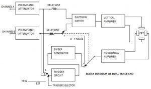
The block diagram of dual trace oscilloscope is shown below:

Digital Oscilloscope: Block diagram of dual trace CRO

For each of A and B signal, A separates preamp will pre-amplify and then it gets attenuated by an attenuator. The amplitudes of each i/p are precisely controlled. After preamplification, both of these signal feed to a switch and capability to pass single channel at a time thru a delay to the perpendicular amp. The time-based circuit utilizes the trigger select switch S2 and permits to be triggered by A or B individually by line freq. or by setting an exterior signal. The horizontal amp is feed via S1/ S3 /switch by the sweep generator.

Explain the function of Aquadag:

An aquadag is basically name used for trading as a water based colloidal graphite widely utilized in cathode ray tubes.

When electron beam strikes the phosphor screen, secondary electrons are emitted from the surface of the screen, and they get accumulated there unless they are removed. When their accumulation becomes quite large, they start repelling the electron beam away from the screen, which will create distorted images on the screen.

To prevent the above problem, in all modern CRO’s a conductive graphite coating called aquadag is deposited on the inner wall of the flared end of the CR tube. This coating is also kept at high positive potential as the accelerating anode. This will perform two functions;

  • The aquadag coating is positive and so it attracts the secondary electrons and keeps removing them eventually.
  • Since the aquadag is installed in front of the anode, it assist e- acceleration to the CRO screen.

What is Digital Storage Oscilloscope (DSO)?

Working principle digital oscilloscope:

In an oscilloscope, the i/p signal is applied to the amplifier and attenuator. The oscilloscope has an amplifier and attenuator circuitry as utilized same as conventional one. The attenuator signal is at that point go to the vertical amplifier part for further process.

A DSO has three modes of operation –

  1. Roll Mode – Here in this mode of operation very frequently changeable signals are displayed clearly in this mode.
  2. Store Mode – this is also termed as refresh mode. Here, input initiates trigger circuit.
  3. Hold or Save Mode – this is automatic refresh mode.

What is Deflection Factor or Deflection Sensitivity?

Deflection sensitivity:

For CRO, it is represented as the deflection of the screen per unit deflection-voltage.

Therefore, deflection sensitivity (S),

eq1

Deflection Factor:

Deflection factor of a CRT is expressed as the reciprocal of Deflection Sensitivity

Therefore, deflection factor (G)

eq2

Both of this parameter is used to characterize the CRT.

For more article click here

Klystron: 7 Important Factors Related To It

660px Klystron tube 1952

Cover By : DanielkuehlerTrain Tracks in ZuerichCC BY-SA 4.0

Points of Discussion

Introduction to Microwave Tubes and Klystron

Microwave Tubes: Microwave tubes are devices which generate microwaves. They are the electron guns which produces linear beam tubes.

660px Klystron tube 1952

Microwave Tube

Image Credit: Unknown authorUnknown author, Klystron tube 1952, marked as public domain, more details on Wikimedia Commons

Microwave tubes are generally divided into categories on the type of electron beam-field interaction. The types are –

  • Linear beam or “O” type
  • Crossed-field or “M” type

Linear-beam: In this type of tube, the electron beam traverses through the tube’s length, and it is parallel to the electric field.

Crossed-field: In this type of tube, the focusing field is perpendicular to the accelerating electric field.

Microwave tubes can also be classified into amplifiers or oscillators.

Klystron: Klystron is a type of microwave tubes which can amplify the higher range of frequencies, especially from Radio Frequencies to Ultra High frequencies. Klystrons can also be used as Oscillator.

Know about Transmission Lines and waveguides. Click Here!

Klystron Amplifier

In an amplifier, the electron beam is sent through two or more resonant cavities. The very first cavity receives the RF input and bunches it into high- and low-density regions to modulate the signal. The bunched beam then goes to the next cavity, which accentuates the bunching effect. In the following or final cavity, the RF’s power is extracted at a highly amplified level.

The two cavities generate about 20 dB of gain, and using four cavities may produce up to 80-90 dB of gain. Klystron amplifiers can peak powers in the range of megawatt. It has power conversion efficiencies of about 30% to 50%.

Operation of Klystron Amplifier

Klystron amplifiers amplify the Rf signal. It converts the kinetic energy of the signal in a DC electron beam into the RF power. Inside a vacuum, an electron gun emits a beam of electrons, and the high-voltage electrodes accelerate the electron beam.

Then, an input cavity resonator accepts the beam. Here some series of operation occurs. At first, the input cavity is fed with RF energy. It creates standing waves. The standing wave further produces oscillating voltages which function on the beam of an electron. The electric field bunched the electrons.

Every bunch enters into the output cavity when the electric field decelerates the beam by opposing the electron’s motion. That is how the conversion of kinetic energy to the potential energy of the electrons occurs.

Reflex klystron and Working of Reflex klystron

Reflex Klystron: Reflex klystron is a klystron with a single-cavity which acts as an oscillator by using a reflector electrode next to the cavity to deliver positive feedback through the electron beam. Reflex klystrons can be tuned mechanically to adjust the cavity size.

Klystron

Reflex Klystron

Image Credit: ErbadeVarian V-260 modelCC BY-SA 3.0

A reflex klystron is often called “Sutton Tube” after the name of scientist Robert Sutton, one of the Reflex klystron inventors. It is a low power klystron with applications as a local oscillator in some of the radar receivers.

Know about 7+ Applications of Microwave Engineering and Overview. Click Here!

Working of Reflex Klystron

Klystron
A Diagrammatic structure, Image Credit: Reflex.sch.enpCC BY-SA 3.0

In a reflex klystron, the electron beam is passed through the only cavity present in the klystron. After the pass, they get reflected by a reflector of a negatively charged electrode. They make another pass through the cavity. Then they are collected. When the electron beam has their first pass, they are velocity modulated. The electron bunches are formed inside the drift space of the reflector electrode and the cavity.

The reflector voltage is tuned to ensure the maximum branching. The electron beam gets reflected by the reflector and re-enters into the cavity. The maximum branching makes sure that the maximum amount of energy is transferred from the beam of an electron to the radio frequency oscillation. The electronic range of tuning of a reflex klystron is typically referred to as the change in frequency between two half PowerPoint.

Applications of Reflex Klystron

Some of the reflex klystrons are listed below.

  • One of the significant applications of reflex klystrons is in Radio and RADAR systems as the receivers.
  • They are also used as signal generators.
  • Reflex klystrons can be used as Frequency modulators.
  • Also, they can be used as pump oscillator and local oscillators.

Nowadays, most of the applications of reflex klystron has been replaced by semiconductor technologies.

Gyroklystron

Gyroklystron is one of the types of microwave amplifier whose working is almost the same as of a klystron.  But for a Gyroklystron, unlike a klystron, the bunching of an electron is not axial. Instead, the modulation forces change the cyclotron frequency, and thus the azimuthal part of the motion creates the phase branching.

At the last or the output cavity, the received electrons transfer their energies to the cavity electric field, and the amplified RF signal can be coupled off from the cavity. The cavity structure of a Gyroklystron is cylindrical or coaxial.  The main advantage of a Gyroklystron over a normal klystron is that a Gyroklystron is capable of delivering high power at high frequencies which is very difficult for a typical klystron.

Optical Klystron

Optical klystrons are the devices where the method of amplification inside is the same as of a klystron. The experiments are done primarily on lasers at optical frequencies, and they are known as Free Electron Laser. These types of devices use ‘undulators’ in the place of microwave cavities.

Two Cavity Klystron

Two cavity klystron is the simplest type of klystron available. As the name suggests, this type of klystron has two microwave cavities. They are known as ‘catcher’ and ‘buncher’. If the two cavities klystron is used as an amplifier, the buncher receives the weak microwave signal and couples out from the catcher, and it gets amplified.

Working of a Two Cavity Klystron

In this klystron, there is an electron gun which generates electrons. An anode is placed at a certain distance from them. Electron gets attracted by the anode and passes through them with high positive potential. An external magnetic field, outside the tubes, produces a longitudinal magnetic field along the beam axis. It helps to stop the beam from the spreading.

The electron beam first goes through the ‘buncher’ cavity. There are grids on both sides of the cavity. The electron beam produces excitation to the standing wave oscillations, which further causes an oscillating AC potential across the grids. The field’s direction varies two times for a single cycle. Electrons enter the cavity when the entrance grid is negative and exits when the exit grid is positive. The field affects the motion as it accelerates them. After the change of direction of the field, the motion of the electrons gets decelerated.

After the ‘buncher’ cavity there, coms the drift space’. The bunching of electrons occurs here as the accelerated electrons get bunched with the decelerated electrons. The length is made precisely so that the maximum branching occurs.
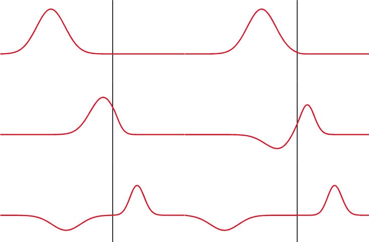
Then comes the ‘catcher’ cavity. It has similar grids on each side. The grids

absorbs the energy from the electron beams. Like the ‘buncher’ here, the electron moves due to the electric field’s change of direction and thus the electrons work. Here the kinetic energy produced by their movement is converted into potential energies. The amplitude of the oscillating electric field is increased to do so. That is how the signal of the ‘buncher’ cavity is get amplified in the ‘catcher’ cavity. Specified types of waveguides and transmission lines are used to couple out from the catcher cavity.

Klystron vs Magnetron (Difference between the Klystron and Magnetron)

To find out the differences between the Klystron and Magnetron, we have to know about the Magnetron.

Magnetron: Magnetron is a type of vacuum tube which generates signals of the microwave frequency range, with the help of interactions of a magnetic field and electron beams.

Points of DiscussionKlystronMagnetron
DefinitionKlystron is a type of microwave tubes which can amplify the higher range of frequencies, especially from Radio Frequencies to Ultra High frequencies.The magnetron is a type of vacuum tube which generates signals of the microwave frequency range, with the help of interactions of a magnetic field and electron beams.
Frequency of operationThe operating frequency range for Klystron is 1 GHz to 25 GHz.Working frequency range is 500 MHz to 12 GHz.
EfficiencyThe efficiency is around 10% to 20%.The efficiency of the magnetron is relatively high, and it is around 40% to 70%.
Output PowerOutput power ranges between 1 milli-watt to 2.5 watts.Output power ranges between 2 mW to 250kW.
Injection of ElectronsElectrons usually are injected from outside.Electrons are injected forcefully from the outside.
Traversing path of the ElectronsElectrons traverse linearly along the axis.Electrons traverse spirally along the axis.
UsabilityCan be used as an amplifier as well as an oscillator.Can be used as Oscillator only.
ApplicationsKlystrons are used in RADARS, like particle accelerators, transmitters, etc.Magnetrons are used in many types of home appliances, including microwave ovens, special heaters.

SWR Meter: 9 Important Explanations

swr meter

Cover Image BY: Theonlysilentbob at English Wikipedia, CC BY-SA 3.0, Link

Points of Discussion

Introduction to SWR Meter | What is an SWR meter?

To know about Standing Wave Ratio Meters, we should know what is SWR at first. SWR is an Acronym of “Standing Wave Ratio”, and it is defined as follow.

SWR or Standing Wave Ratio: Standing Wave ratio is defined as the ratio of the maximum RF voltage to the minimum RF voltage of a transmission line.

When the ratio is calculated with respect to the AC voltage, then the parameter will be called voltage SWR, and if the ratio is calculated with respect to current, then the SWR will be known as current SWR.

Standing waves are physically stationary waves but not like typical ones as the amplitude doesn’t change with respect to time. SWR is necessary for the measurement of impedance matching for loads of transmission lines in Microwave Engineering.

What is an SWR Meter?

SWR Meter: SWR Meter or Standing Wave Ratio meter or Wave Ratio Meter or VSWR Meter (Voltage Wave Standing Ratio Meter) measures the value of Standing Wave ratio of a transmission line.

330px Para dynamics swrmeter dec07
A typical Standing Wave Ratio Meter, Image BY: Theonlysilentbob at English Wikipedia, CC BY-SA 3.0, Link

The Standing Wave Ratio Meter actually measures the amount of mismatch present between the load and the transmission line associated with it. It also determines the amount of RF energy reflected by the transmitter.

The most common type of standing wave ratio meter contains a dual directional coupler which other samples out some amount of power in a direction. After that, a diode does some rectifications and applies to the meter.

This method of operation finds out a comparison between the minimum and maximum level of voltages. The standing wave ratio meters is applicable and useful for signal ranging from very high frequencies and above. It cannot be used for low-frequency signals.

VSWR meters measures voltage Standing Wave Ratio and ISWR meters measure current standing wave ratio.

Methods of Measurement of SWR

There many different methods available for measurement of SWR. The simplest method is the method of using a slotted line. The slotted line is a part or component of transmission lines with an uncluttered slot through which a probe gets passed. The probe does the main thing by allowing to measure voltages at various points.
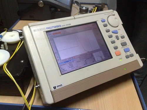
Real World Applications of SWR Meter

Standing Wave Ratio Meter is one of the most critical and crucial devices for Microwave Engineering. SWR meters are widely used for setting up Antennas and connecting the antennas with their transmission lines. SWR Meters are also used for medical applications which are based on microwave engineering.

Know about Transmission Lines and waveguides. Click Here!

Working of an SWR Meter | How does an SWR work?

Let us discuss how an SWR Meter works or how a directional SWR works. A directional SWR meter is necessary to measure the amplitude of the transmitted wave as well as the amplitude of the reflected wave.

Directional SWR Meter
Directional SWR , Image Credit: InductiveloadSWR Meter, marked as public domain, more details on Wikimedia Commons

As the image shows, there is a transmitter (Tx) and an antenna (ANT) terminal connected with the help of a transmission line. Here, the significant line electromagnetically couples with the directional couplers. Resistors terminate the lines at one of the ends and diodes are connected at another end for rectification purposes.
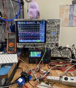
The resistors help to match the characteristic impedance of the transmission lines, and the diodes allow the conversion of the amplitudes of waves to their equivalent DC voltage. At last, capacitors smoothen the final DC voltage. There are also connected amplifiers with the forward and reverse terminals. They function as the needed drain resistor and help to determine the Dwell Time.

Know about Rectangular waveguides. Click Here!

How to use an SWR meter?

VSWR meters or typical Standing Wave Ratio meters are easy to use and measure the standing wave ratio. The process of using an Standing Wave Ratio meter while doing an experiment or applying for other purposes are listed below. The steps will help to interpret the result from the meters.

An important point to be noted before using VSWR is that: VSWR should be used at low power and in the clear channel, primarily if the experiment aims to measure an antenna’s performance.

  • Step 1: Find a clear frequency channel – The frequency channel should be clear enough or noiseless enough so that the transmitted signal from both ends could be interpreted from both sides.
  • Step 2: Reduction of Power – The transmitted power should not exceed a specific power range so that the signal causes distortion at the output devices.
  • Step 3: Set up the Mode – The mode of operation should be set using the options available on the meter. Like – Amplitude Modulation, Frequency Modulation etc.
  • Step 4: Set up of Meter – Now we need to set the Standing Wave Ratio meter to the forward mode. To do so, check the front panel. Also, switch the adjustment knob downwards. It will help to restrict overloading.
  • Step 5: Adjustment of the Forward Reading – After the transmitter starts its transmitting job, keep adjusting the CAL knob to ensure a full-scale reading of the experiment.
  • Step 6: Set up of Meter – Now the Standing Wave Ratio Meter is set up again. This time the knob on the front panel is changed to ‘Reverse’ direction. This is done after the meter is set for forwarding power.
  • Step 7: Restrict the transmission – The transmission is stopped as soon as possible to restrict the VSWR meter’s overloading.
  • Step 8: Repeat the above steps for various frequencies – Took the readings for several other frequencies by following the same steps.

SWR Bridge

Impedance bridge is also capable of measuring Standing wave ratio. Impedance bridge is an LCR meter. When the given impedance gets matched with the reference impedance, the bridge gets balanced. If a transmission line gets mismatched, there is some deviation of input impedance, and that could lose the bridge’s balance. That is how a bridge can measure if there is some amount of SWR present in the connection.

Know about 7+ Applications of Microwave Engineering and Overview. Click Here!

SWR Meter Reading Explanations

Let us discuss the reading collected by Standing Wave Ratio Meters. Different values of Standing Wave Ratio meters describe different conditions.

Range of valueExplanation
SWR 1 to 1.5It is considered as the ideal range of value. The reading can be decreased to 1 from 1.5 by doing some additional tuning.
SWR 1.5 to 1.9It is not the best range, but fair enough. Such readings come from vehicle variables or installations faults. It is an acceptable range.
SWR 2.0 to 2.4It is not a good range of value. There are scopes for improvement. This range of values come from poor antenna mounting location. Fixing that problem might improve your meter’s SWR value.
SWR 2.5 to 2.9This range of value affects performance and lead to wrong impressions. The transmitter may also get a damaged—poor quality of equipment and needy mounting causes this range of values.
SWR >  3Operation with this range of values is risky. The device will be damaged within a few moments. The transmission should be stopped at this range. The reason behind such worse values is major installation problems. Attach a proper ground with the device. This range can also indicate poor quality of antenna and faulty coaxial cables.

Point to be noted: Do not transmit a signal if the SWR range exceeds the range of 1.5 to 2. It will damage the transmitter. If you observe the reading is more than 2.5, shut down the transmitter as soon as possible.

Essential Formulas For calculation of SWR using SWR Meter

The formula for calculating VSWR is Vmax / Vmin.

Also, the expression for VSWR using the forward and reverse wave voltages can be written as: VSWR = (VFWD + VREV) / (VFWD – VREV)

There is another formula for calculation of SWR.

SWR = | 1 + Г| / | 1 – Г|

Digital SWR Meter

Nowadays, most of the analogue SWR meters are replaced by Digital SWR Meters. Digital SWR Meters are easier to use, take less time to get the result, smaller in size, and lower the maintenance cost than an analogue meter.

Limitations of Standing Wave Ratio (SWR) Meters

SWR Meters does not measure the physical impedance present for a load. Instead, it measures a ratio which gives us the idea of mismatch. The perfect impedance for the load can be measured using a separate device known as – “Antenna Analyzer”.  The measurement is only possible if the SWR meter is set perfectly with the transmission line itself. It is matched with the characteristic impedance of the transmission line (generally 50 to 70 ohms).

SWR meters must be set up as close as possible concerning the transmission line. Otherwise, SWR creates some false impression regarding the readings.

Rectangular Waveguide: 5 Important Facts

RW 1 1

Points of Discussion

Introduction to rectangular waveguide

Rectangular Waveguides are one of the primarily used transmission lines. The primary application of rectangular waveguides was the transmission of microwave signals. It has still some critical applications. Some of the components like – couplers, detectors, isolators, attenuators, and slotted lines are available in the market with their large variety for different waveguides band ranging from 1 to 22o GHz. Nowadays, modern devices are using planar transmission lines like stripline or microstrips rather than waveguides. It also helps the miniaturization of the devices. However, the waveguides still have significant applications, including high-power systems, millimetre wave applications, satellite systems, etc.

Rectangular waveguides of a hollow structure can propagate TE (transverse electrical) modes and TM (transverse magnetic) modes but not the TEM (transverse electromagnetic) modes. The reason behind such characteristics is the single conductor. This article will discuss the transmission of TE and TM modes and find out several properties of them.

Know about Transmission Lines and waveguides. Click Here!

TE Modes on Rectangular Waveguide

As we know, TE modes of waveguides are specified by Ez = 0 and hz will satisfy the reduced wave equation. The reduced wave equation is given below.

RW 1 1

Here, the cut off number is the kc. It is given as: kc = √ (k2 − β2) and Hz (x, y, z) = hz (x,y) e – jβz.

Now, the above equation can be solved using the method of separation of variables. Let, hz (x,y) = X (x) Y(y)

Substituting the hz in the equation, we get:

RW 2 1

Following the usual separation of variables, as each of the terms must be equal to a constant, we provide separation constant kx and ky. Now, the equations are:

RW 3 1

The constants also satisfy another condition. That is: kx2 + ky2 = kc2

The typical solution for hz comes as:

hz (x, y) = (A coskxx +B sinkxx) (C coskyy + D sinkyy).

To determine the constant value, boundary conditions have to apply on the electric field components in tangential direction to the waveguide’s wall. They are given below.

ex (x, y) = 0 for y= 0 and b.

ey (x, y) = 0 for x= 0 and a.

The values of ex and ey from hz comes as below. They are calculated from some other wave equations.

RW 4 1

From the boundary conditions of ex and evaluated value of ex, D’s value comes as 0 and ky = nπ/b for n = 0, 1, 2…

Also, from the boundary conditions of ey and evaluated value of ey, B’s value comes as 0 and kx = mπ/a for m = 0, 1, 2…

At last, the solution of Hz comes as:

Hz (x, y, z) = Amn cos (mπx/a) cos (nπy/b) e – jβz

Here, Amn is an arbitrary amplitude constant which is made up of the constants A and C.

Now, the transverse field components of TEmn modes are specified below.

RW 5

The propagation constant is given by:

β = (k2 – kc2)1/2 = (k2 – (mπ/a)2 – (nπ/b)2)1/2

Now, in reality, k > kc,

β = [(mπ/a)2 + (nπ/b)2]1/2

Now each mode (for each combination of m and n) has a cutoff frequency. It is specified by fcmn.

fcmn = kc/ (2π√µe) = (1/(2π√µe) * [(mπ/a)2 + (nπ/b)2]1/2

The mode having the lowest cutoff frequency is known as dominant mode. In the dominant mode, we assume that a > b. the minimum cut off frequency happens for the TE10 mode and cutoff freq. expressed as:

 fc10 = 1 / (2a√µe)

TE10 is the overall dominant mode for TE mode. Now for m = n = 0, all the expression comes to 0. That is why there is no TE00 mode.

The wave impedance with the relation of the transverse magnetic field and transverse electric field comes as ZTE = Ex / Hy = Ey / Hx = kη / β

Here, η = √µ/e. It is the intrinsic impedance of the material present inside the waveguide.

There is another important parameter present known as guide wavelength. It is defined as the difference between two equal-phase along the waveguide. The difference here means the distance. Guide Wavelength can be calculated as

λg = 2π / β > 2π / k = λ

Wherever, λ is the wavelength of a plane wave which is present in between the guide.

The following expression gives the phase velocity.

υp = ω / β > ω / k = 1 / (√µe)

It is greater than the speed of light.

Know about 7+ Applications of Microwave Engineering and Overview. Click Here!

TM Modes on Rectangular waveguide

We know that TM modes are characterized by Hz = 0. And the Ez component must satisfy the reduced wave equation.

RW 1 2

Here, Ez (x, y, z) = ez (x, y) e -jβz. Here, the cut off number is the kc. It is given as kc = √ (k2 − β2).

The solution is achieved using the same process as that of TE mode. The typical solution of ez comes as:

ez (x, y) = (A coskxx +B sinkxx) (C coskyy + D sinkyy)

Now, applying the bounding conditions, which are listed below, we get –

ez (x, y) = 0 for x= o and x = a,

and, ez (x, y) = 0 for y = 0 and y = b.

Now, from the boundary conditions of ez and evaluated value of ez, the value of A comes as 0 and kx = mπ/a for m = 0, 1, 2…

Also. from the boundary conditions of ez and evaluated value of ez, the value of C comes as 0 and ky = nπ/b for n = 0, 1, 2…

At last, the solution of Ez comes as:

Ez (x, y, z) = Bmn sin (mπx/a) cos (nπy/b) e – jβz

Here, Bmn is an arbitrary amplitude constant which is made up of the constants B and D.

The calculated transverse components for the TMmn modes are listed below.

RW 6

The propagation constant is given by:

β = (k2 – kc2)1/2 = (k2 – (mπ/a)2 – (nπ/b)2)1/2

For TM modes, the dominant mode is TM11 as the other lower mode like TM00, TM01 or TM10 is not possible as the filed expressions become zero. The cutoff frequency for the dominant mode is given as: fcmn.

fc11 = (1/(2π√µe) * [(mπ/a)2 + (nπ/b)2]1/2

The wave impedance with the relation of transverse magnetic field and transverse electric field, comes as: ZTM = Ex / Hy = – Ey / Hx = ηβ / k

Solved Example on Rectangular Waveguide

1. A rectangular waveguide is filled up with Teflon, and it is copper K-band. The value of a = 1.07 cm and b = 0.43 cm. The operating frequency is 15 GHz. Answer the following queries.

A. Calculate the cut-off frequencies for the first five propagating nodes.

B. compute the attenuation because of dielectric and conductor loss.

Solution:

The permeability of Teflon is 2.08. tan delta = 0.0004

We know that the cutoff frequencies are:

fcmn = (c/(2π√µe) * [(mπ/a)2 + (nπ/b)2]1/2

Now, the values for different m and n values are calculated using the formula.

The below list shows the values.

value

The first five modes those will propagate through the rectangular waveguide are TE10, TE20, TE01, TE11 and TM 11.

At 15 GHz, k = 453.1 m-1.

The propagation constant for TE10 comes as:

β = [ (2πf√er/c)2 – (π/a)2] ½ = [k2 – (π/a)2]1/2 = 345.1 m-1

The attenuation from dielectric loss: αd = k2 tan δ / 2β = 0.119 Np/m

Or, αd =1.03 dB/m.

The surface resistivity of the copper (conductivity is 5.8 x 10⁷ S/m) walls are:

Rs = √(ωµ0/2σ) = 0.032 ohm.

The attenuation from the conductor loss:

αc = (Rs / a3bβkη) * (2bπ2 + a3k2) = 0.050 Np/m = 0.434 dB/m.

Characteristic Table of Rectangular Waveguide

characteristic table of rectangular waveguide
Characteristic table of rectangular waveguide

Cover GIF by: L’OFFICIEL MARTINIQUE