DC Circuits | 5+ Important methods of analysis

KCL

Points of Discussion : DC Circuits

  1. Introduction to DC Circuits
  2. Kirchhoff’s Laws
  3. Kirchhoff’s Current Law (KCL)
  4. Kirchhoff’s Voltage Law (KVL)
  5. Node Voltage Method
  6. Mesh Current Method
  7. Loop Current Method
  8. Some Important Questions related to DC Circuits

Introduction to DC Circuits

DC stands for Direct Current. If the energy source phase doesn’t change with time, then the circuit will be referred to as DC Circuits. Primary energy sources for DC Circuits are batteries or similar steady power suppliers. They have a range from 5 Volts to 24 Volts. Seeing the energy symbol of a circuit, one can understand whether it is AC Circuit or DC Circuits. The symbols are given below.

Kirchhoff’s Laws

Gustav Robert Kirchhoff was an eminent physicist of German origin. His research related to electrical circuits gave us two primaries yet the most critical laws for circuit analysis. These laws are typically known as Kirchhoff’s laws. He had come up with laws for both current and voltage. They are popularly known as – Kirchhoff’s Current law and Kirchhoff’s Voltage Law. These laws are fundamental rules for DC circuits analysis.

Before studying Kirchhoff’s laws, one should have basic circuit properties of nodes, junctions, loops, mesh, branches, etc. Some definitions are given below; please check the circuit analysis article for more such primary terminologies.

  • Node / Junctions: Node or junction in a circuit is known as the connecting point of two or more numbers of components.
  • Loop: A loop in a circuit is defined as a closed path starting from a specific node, traveling through any part of the circuit, and ends at that specific point. There is a point to be remembered that the path can travel any circuit part only for once.  A loop can include or overlap with any other loop of the circuit.
  • Mesh: Mesh can be said as the smallest loop possible in a circuit that has no overlap and doesn’t include any other loop within it.
  • Kirchhoff’s Current Law is often interpreted as the First Law of Kirchhoff’s or Kirchhoff’s Junction law. It deals with the current equations of a node or junction.
  • Kirchhoff’s Voltage law is often interpreted as the Second Law of Kirchhoff’s or Kirchhoff’s loop law. It deals with the voltage equations of a loop.

Kirchhoff’s Current Law (KCL)

“Kirchhoff’s current law states that the summation of the incoming current to a node is equal to the summation of the outgoing current from the node.”

Mathematically it can be stated as the following equation.

∑Iin = ∑ Iout

DC Circuits, KCL
DC Circuits, Image – 1

From the above image, we can observe that the currents I1 and I4 are incoming to the node while I2 and I3 are outgoing currents. So, we can write according to Kirchhoff’s Current Law that –

I1 + I4 = I2 + I3

Or, I1 + I4 – I2 – I3 = 0

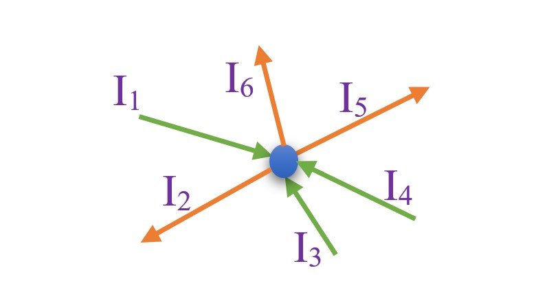
Concept Check: What will be the current value for the branch I5? Provided that I1= 2 mA, I2= 1 mA, I3= 4 mA, I4= 1 mA and I6= 2 mA.
DC Circuits, KCL
DC Circuits, Image – 2

Solution: To solve this type of problem of DC Circuits, first find out the desired node. Then separate the incoming and outgoing current components. Then apply Kirchhoff’s current law and find out the solution.

The incoming currents are I1, I3, I4.

The outgoing currents are I2, I5, I6.

The missing component is I5, which is outgoing.

Now, from KCL, we know that –∑Iin = ∑ Iout

So, we can write –

I1 + I3 + I4 = I2 + I5 + I6

Or, I5 = I1 + I3 + I4 – I2 – I6

Or, I5 = 2 mA + 4 mA + 1 mA – 1 mA – 2 mA

Or, I5 = 4 mA

Kirchhoff’s Voltage law (KVL)

Kirchhoff’s Voltage Law states that the voltage around a loop of the circuit equals zero, and the algebraic sum of voltage drop at each branch in that loop is equal zero also.

Mathematically it can be stated as the following equation.

Vn = 0

Vn represents the voltage around n elements or branch of the loop.

DC Circuits, KVL
DC Circuits,
Image Credit – KwinkunksKirchhoff voltage lawCC BY-SA 3.0

From the above image, we can write that,

VAB + VBC + VCD + VDA = 0

Kirchhoff’s voltage law has few characteristics. Some of them are –

  • While analyzing a circuit, if you start your path with a node, do not include any other loop in your path, and end your path in the same node, then the sum of voltage through that path will be zero.
  • The path can be in any direction; the Clockwise or anti-clockwise path does not affect Kirchhoff’s voltage law.
  • A typical complex circuit may have many loops. KVL is valid for each and every possible loop of the circuit.

Node Voltage method

The node voltage method is another useful method for the analysis of the DC circuit. It is derived from Kirchhoff’s current law. SPICE – a simulator software contains this method. Actually, this method is more comfortable to implement and analyze the whole circuit. Using the method helps us to get rid out of Kirchhoff’s voltage law if we want to.

  • Node Voltage: Node voltage is a concept needed for the Node Voltage Method. This can be defined as the potential difference between two nodes.

Steps to follow: The node Voltage method can be applied to the DC circuits by following the below-mentioned steps.

  • Select a reference node. In most cases, the ground node is elected.
  • Name all the other nodes of the circuit.
  • Start with the nodes, which seems to be easy. The energy source (preferably voltage source) node connected with the reference node would be more comfortable.
  • Now apply Kirchhoff’s current law for every node. Also, do the calculations of hm’s law.
  • Find out the solutions for all of the node voltages.
  • Find out any current of the circuit with the help of Ohm’s law.

Mesh Current Method

The mesh current method is another efficient method for DC circuit analysis. It is derived from Kirchhoff’s Voltage Law, and a new method named “Loop current method” is derived from this method. It has an added advantage over other circuit analysis methods as it does not require to solve a 2E number of circuit equations (E stands for the number of elements of the circuit). Studying this method needs an adequate level of understandings of the concept of loops and meshes.

  • Loop current: Loop current is a concept needed for this method. It is defined as the current through any loop or mesh of the circuit.
  • Superposition principle: Superposition stands for general addition. Here superposition principle states that loop currents can be added together to get the actual current element.
  • Linearity: Linearity characteristics help to use the principle of superposition. Linearity is multiplying voltage with a constant and getting the current as constant the multiplied product.

Steps to follow: Mesh current method can be applied by following the below-mentioned steps.

  • Mark the meshes (known as open windows of the circuit).
  • Choose a specific constant current direction (either clockwise or anti-clockwise), which all be applied for every mesh. Also, give current variables to each mesh.
  • Apply Kirchhoff’s Voltage law for each mesh and write down the equations.
  • Calculate the resulting system for all the mesh equations.
  • Using Ohm’s law, find out the desired current and voltage components.

Loop current Method

We can say that the Loop current method is an updated version of the Mesh Current method. This method is popular and helpful for non-planar circuits.

Steps to follow: loop current method can be used to analyse DC circuits using the below-mentioned steps.

  • Mark the meshes (known as an open window of the circuit). Also, identify the loops.
  • Choose a specific constant current direction (either clockwise or anti-clockwise), which all be applied for every mesh. Also, give current variables to each mesh or the loops.
  • Calculate the resulting system for all the mesh and loop current equations.
  • Using Ohm’s law, find out the desired voltage and current component.  

Some important questions related to DC Circuits

1. What is the main idea behind Kirchhoff’s current law?

Answer: The main idea behind Kirchhoff’s current law is the theory that charges cannot be accumulated at one point.

2. Write some limitations of Kirchhoff’s laws.

Answer: Kirchhoff’s both laws have some limitations. They are listed below.

  • Kirchhoff’s current law comes with the assumption that conductors and wires are the only media for the flow of current. In reality, in high-frequency circuits, we can observe the flow of current in open circuits as standard conductors work as transmission lines.
Transmission line animation3
KCL is violated in Transmission Lines, Dc circuits, image – 4 Image Credit – Sbyrnes321Transmission line animation3CC0 1.0
  • Kirchhoff’s Voltage law comes up with the assumption that every closed loop of the circuit will be free from the effect of the magnetic field, more specifically, the fluctuating magnetic field. But, in the high-frequency circuits, this condition doesn’t get satisfied.

3. Nodal analysis is based on the law of energy conservation—state whether the given sentence is true or false.

Answer: False. Nodal analysis is based on Kirchhoff’s current law, and also Kirchhoff’s first law supports the conservation of charges, not energy.

4. What is the effect on the circuit’s current if the energy sources are connected in parallel?

Answer: The current of the whole circuit gets increased.
MOS Transistor: 3 Important Facts You Should Know

1920px MOSFET functioning.svg 300x162 1

Topic of Discussion: MOS Transistor

What is MOS Transistor?

A Metal-Oxide-Semiconductor or ‘MOS’ transistor is recognized for its operation as an ideal switch operation.  A MOS transistor chip performs as a reliable current and capacitor of the transistors and its wires.

1920px MOSFET functioning.svg
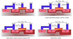
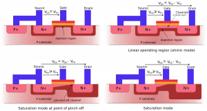
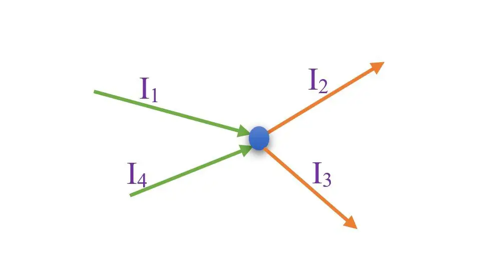
a MOS structure in Inversion, Saturation and Depletion region, Image credit – Olivier Deleage and Peter Scott, MOSFET functioningCC BY-SA 3.0

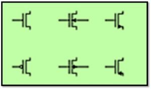
In the figure below, we can see some regular schematics of MOS transistors that are used commonly

MOS transistors
regular schematics of MOS transistors

We typically use the different terminal symbols i.e., figure when the body along with the substrate or the well-connection needs to be shown.

Working Principle of MOS Transistor:

For being a majority carrier device, a MOS transistor carries the current between its source and drain. This transistor gets regulated with a regular voltage applied to the gate of the respective MOS. In an n-MOS transistor, the electrons act as a the majority carrier while in a p-MOS type, Holes is acts as majority carriers. A MOS transistor is examined with an isolated MOS structure with a gate and body included to know about its properties or behavior’s figure below gives a simple structure of MOS. The top most layer of the MOS structure is made of a conductor.

This is very good for carrying currents for any charge; which is acknowledged as the gate. The transistors which were made at the very beginning, used metal gates; with the up growing time period, the transistor gates were changed and polysilicon is being used. The intermediate mid-layer of a MOS is made of a thin insulating film of silicon oxide which is usually identified as the gate oxide. The layer at the lower level is doped with silicone.

If we apply a negative voltage in the gate, a negative charge on the gate is produced. Beyond the gate, the holes are attracted toward the region as the mobility carriers are charged with positive energy. This is called the accumulation mode.

In figure (b), a A very minimal amount of voltage is supplied to the gate, which we get from a positive charge on the gate. To form a depletion region, the holes of the body which are generated from repulsion, get accumulated under the gate.

In figure (c), Threshold Voltage Vt is supplied and few electrons gets attached to that area.

Inversion Layer:

The conductive layer of the electrons in the p-type body is considered as an the ‘inversion layer’.

Here, the threshold voltage depends on two parameters, they are –  1. MOS’s dopants 2. Oxide layer’s thickness. It is regularly positive but they also can be made into negative ones. The nMOS transistor has piles of MOS between both the n-type regions called the source and the drain.

At this point, the gate-to-source voltage Vgs < the threshold voltage (Vt). The source and drain are having no of free electron in both sides. When the source is not working i.e., in ground state, the junctions are said to be reverse-biased, so no current flows. When the transistor is said to be OFF, this mode of operation is called cut-off.

the current is 0 if we compare it with an ON-transistor. The gate voltage is higher than the threshold voltage. Now if an inversion region of electrons which are the channel, makes a bridge between the source and drain and create a conductive path and turns the transistor ON. The increase in the number of total carriers and the conductivity increases are proportionate to each other with respect to the applied gate voltage.

The drain voltage – Source voltage is given as:

 VDS = Vgs – Vgd . When, VDS = 0 (i.e., Vgs = Vgd),

there is no such electric field exists to produce current from drain to source.

Threshold formation nowatermark 1
 Inversion channel and attainment of threshold vol­tage (IV), Image Credit – Saumitra R Mehrotra & Gerhard Klimeck, modified by ZephyrisThreshold formation nowatermark, marked as public domain, more details on Wikimedia Commons

When, The voltage (Vds ) is applied to the drain, and the current Ids carries through the channel of drain to the source. If Vds becomes larger than that Vgd < Vt, the channel doesn’t seem to have any change near the drain and hence it is in off state. Even after this, the conduction is being continued with the help of the drifted electron which is generated by the +ve voltage.

 When the electrons reached to the termination of the channel, the depletion region adjoining the drain gets accelerated in the direction of it. The injected electrons accelerate this process.

Saturation Mode:

In this mode, the current Ids is controlled by the gate voltage and gets terminated by the drain only when it reaches beyond the drain voltage.

V-I Characteristics of MOS Transistor

The V-I characteristics of MOS transistor has three regions of operation:

  • The Cut-off or sub-threshold region.
  • The Linear region.
  • The Saturation region.

The length of channel in an n-MOS transistor is lengthier and the electric field amongst the source to drain is comparatively low. The channel is generally identified as the ‘long-channel’, ideal, 1st order, or Shockley model while characterized as a figure.

The long-channel model represents a current that carries through an OFF transistor. It is very low or 0.  The gate attracts carriers to build a channel in its OFF state (Vgs> Vt). At the source to drain region, the electrons keep flowing at a uniform speed.

Charge of the capacitor plate is given by – Q = CV.

Thus, the charge in the channel Qchannel is

                                    Qchannel = Cg(Vgc – Vt)

1920px IvsV mosfet.svg
Image Credit – User:CyrilBIvsV mosfetCC BY-SA 3.0

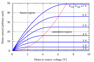
The above graph shows the I-V characteristics for the transistor.

 In the particular graph, the current which flows is ‘0’ for gate voltages underneath Vt. The current has increasing when the gate voltage increases accordingly linearly with V­ds for small Vds. As Vds approaches the saturation point Vdsat = VGT, current declines and eventually turn out to be independent.

 The pMOS transistors behave in a reverse way than the n-MOS transistor  so all voltages and currents are negative here.Here the current flows from source to drain and the fluidity of holes in a silicon is usually lower than that of the electrons.

 So, a p-MOS transistor produces less current than n-MOS transistor of same size and features. Here µn and µp = mobility of electrons and of holes in n-MOS and p-MOS transistors, respectively. The mobility ratio µnp lies between 2–3. The p-MOS transistors have the identical geometry like a nMOS.

For more about MOSFET and others electronics related article  click here

CMOS Amplifier: 5 Important Explanations

CMOS Amplifier 300x60 1

Topic of Discussion: CMOS Amplifier

  • What is CMOS ?
  • What is CMOS Amplifier ?
  • Input Offset voltage
  • Different parameters in CMOS amplifier
  • Applications of  CMOS  Amplifier

What is CMOS ?

CMOS:

CMOS is acronym of Complementary Metal Oxide Semiconductors. It is one of the types of Metal oxide Field Effect Transistor and it is a unipolar device unlike BJTs.

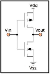
CMOS amplifier: CMOS inverter
CMOS inverter

What is a CMOS Amplifier ?

CMOS Amplifier:

CMOS amplifiers (complementary metal–oxide–semiconductor amplifiers) are universal analog circuits utilized in personal computer, laptops, audiovisual device, mobilephones, cameras, communication systems, different biomedical applications, to many more other applications. In high performing CMOS amplifier circuitry, transistors are generaly used. Transistor not only utilzed to amplify the signals but those are also utilized as active load to attain high gain and output swing in comparison to resistive loading blocks.

The above figure shows a two stage CMOS Amplifier.

Some of the critical parameters which represents the amplifiers are – 1. Range of the supplied voltage, 2. Response to frequencies, 3. Response to the Noises, etc.

Input Voltage Range:

The range designates a “permissible” I/P voltage that will generate a linear, non-distorted O/P signal.

                                          VDS>VGS – VT

VG is the input voltage, VD is VDD -VSAT for PMOS.

From the above explanation, the input voltage is able to swipe to some degree above the voltage VDD. The M15 and M16 are constructed to oppose to that current direction of M14. Nonetheless, VDM12 is not equal to VDM14.

Signal Path of CMOS Amplifier:

Signal-path represents the path through which the signal reaches to the output from the input. The signal path employed to investigate the freq-response, stability, and many more factors.

As the standard CS amplifier has high gain, the Miller effect will increase the total input capacitance. Any capacitance between output and input can be seen as capacitance at the input to the ground with the multiplication of (1 + Gain).

Load in CMOS Amplifier:

We can observe two varieties of active load in CMOS Amplifier: The diode connected MOS or current source MOS.

  1. It represents the output associated with a source of current. The current source acts as ‘Load’ for the output.
  2. By reason of Vgs of the active load is constant. Resistance value is r0 = 1/λId, where Id is drain current. The low frequency or direct current (DC) gain,

                        Av = gmn (roM16 // r0casp) gM17 (r0M18 // r0M17)

Typical load problem:

• Buffer configuration is a severe test for instability. It is found that a need of having a greater compensation capacitor for this purpose.

• It cannot drive a small load resistor.

CMOS Amplifier Parameters:

Input Offset:

The offset voltage is Vref – VI

The offset voltage of the amplifier has presented in above figure. This is measured from the disparities by taking considerations of paramter such as threshold voltage, load resistance, etc.

Common Mode Rejection Ratio (CMRR):

“CMRR is given by the ratio of the gain of the amplifier in differential mode to the gain of the amplifier in common mode.”

Power Supply Rejection Ratio(PSRR):

Power Supply Rejection Ratio or PSRR is given by the ratio of Output voltage to the input voltage. PSRR describe the noise rejection of CMOS amplifier.  Typical method to improves the power supply rejection ratio is generally by by means of a cascode current source or sink (this is because of high output resistance value).

Slew Rate and Settling Rate:

  • High slew rate
  • Small compensation capacitorIncrease the operating current

Settling time is equivalent to Tsettling parameter and

Slew Rate = Vidmax

Noise:

For 1 μA, 7.8 × 10¹² electrons passing every second will generate a noise of 7800 Giga Hertz.

1. The higher input transistor is required to reduce the noise level.

2. Increase in operating current is also required.

3. White and short noise  is mostly constant during the total operation

4. Flicker noise

Compensation in Amplifier:

Compensation is required to ensure stability in opamp. A CMOS Amplifier, loop-gain and phase are the prameter generally specify the Amplifier’s stability. The Op-Amp is generally constructed in a closed-looped for gain and phase analysis puropse. Suitable capacitance, resistance and biasing is also required for the compensation of amplifier.

Uses of CMOS Amplifier:

  • This complementary metal–oxide–semiconductor amplifiers are utilized in personal different electronics consumer products such as computer, laptops, audiovisual device, mobile phones, cameras etc.
  • These are one of the important component of telecom appliance
  • Different biomedical applications utilized these type of amplifier nowadays. There are many more other applications of CMOS amplifier and list is increasing.

For more about MOSFET basics and others electronics related article  click here

Read more about Log & Antilog Amplifier.

Parabolic Reflector Antenna: 7 Interesting Facts To Know

Erdfunkstelle Raisting 2 1024x923 1

Bildnachweis – “Freundschaft an Bord”(CC DURCH-NC-ND 2.0) durch Elf-8

Diskussionspunkte

Einführung in die Parabolreflektorantenne

Antenne oder Strahler ist ein Mittel zum Strahlen und Empfangen elektromagnetischer Informationen. Parabolreflektorantenne ist eine der weit verbreiteten Antennen. Es ist ein besonderer Typ von Reflektorantennen. Der Einsatz von Reflektorantennen begann mit dem Beginn des Zweiten Weltkriegs mit der Weiterentwicklung der Kommunikationstechnologien.

The most straight-forward reflector and more comfortable to implement the reflector antenna is ‘Plane Reflector’ antenna. There are some other types of reflectors also, like – corner reflector, parabolic reflector, Cassegrain reflectors, spherical reflectors. Parabolic reflectors have another type known as ‘Front fed parabolic reflector antenna’.

Was ist eine Hornantenne? Erkunden hier!

Übersicht der Parabolreflektorantenne

Die Strahlungsparameter einer Reflektorantenne können durch Verbesserung des Strukturmusters des Bodens verbessert werden. Auf diesem Gebiet kommt für diesen Parabolreflektor die optische Wissenschaft ins Spiel. Die optische Mathematik beweist, dass einfallende parallele Strahlen durch Reflexion an einer parabelförmigen Struktur zu einem bestimmten Punkt (bekannt als Brennpunkt) konvergiert werden können.

Die reflektierten Wellenformen treten als paralleler Strahl aus. Dies ist ein mathematisches Phänomen, das als “Reziprozitätsregel” bekannt ist. Der proportionierte Punkt wird als Scheitelpunkt bezeichnet. Die ausgehenden, reflektierten Strahlen werden als kollimiert bezeichnet (da sie parallel sind). Obwohl die praktischen Beobachtungen gezeigt haben, dass die austretenden Strahlen nicht als paralleler Strahl bezeichnet werden können, unterscheiden sie sich geringfügig von der richtigen Form.

Der Sender dieser Antenne befindet sich im Allgemeinen an den Brennpunkten der Schale oder des Reflektors. Diese Art der Einrichtung wird als “Front-Feed” bezeichnet. Wir werden im nächsten Teil dieses Artikels eine Analyse dieser Art von Parabolreflektoren diskutieren.

Was macht eine Übertragungsleitung? Erforschen!

Anwendungen der Parabolreflektorantenne

Parabolreflektorantenne

Eine der größten Reflektorantennen in Deutschland für Satellitenkommunikation, Image Credit – Richard Bartz, München aka Makro-FreakErdfunkstelle Raisting 2CC BY-SA 2.5

Parabolreflektoren sind eine der weit verbreiteten, hocheffizienten Antennen, deren Nachfrage von Tag zu Tag steigt. Vom Empfang des Signals für unser Fernsehgerät bis zur Übertragung des Signals für die Raumstationen findet dieser Antennentyp Anwendungen in nahezu allen Bereichen der Kommunikationstechnologie. Einige der bemerkenswerten sind – auf Flughäfen, in Satelliten, in Raumstationen, in Teleskopen usw.

Eigenschaften

Einige signifikante Eigenschaften des Parabolreflektors sind unten angegeben. Die Eigenschaften betreffen Aperturamplitude, Polarisationseigenschaften, Phasenwinkel usw.

  • Der Magnitudenanteil hängt vom Abstand der Einspeisung zur Reflektoroberfläche ab. Die Proportionalität variiert von Struktur zu Struktur. Wie bei einer parabelförmigen Form ist sie umgekehrt proportional zum Quadrat des Radius der Parabel, und bei einer zylindrischen Struktur ist die Beziehung umgekehrt proportional zu ρ.
  • Der Brennpunkt des Reflektors wirkt für verschiedene Arten von geometrischen Konfigurationen unterschiedlich. Die zylindrische Struktur hat eine Linienquelle und parabolische Strukturen haben eine Punktquelle.
  • Wenn der Vorschub lineare Polarisationen parallel zur Zylinderachse aufweist, besteht keine Möglichkeit von Kreuzpolarisationen. Parabolische Strukturen haben nicht die gleiche Eigenschaft.
Parabolic antenna types2
Arten von Parabolreflektor-Feeds, Bildnachweis – ChetvornoParabolantennentypen2, als gemeinfrei gekennzeichnet, weitere Details zu Wikimedia Commons

Überprüfen Sie das Strahlungsmuster von Yagi Uda Antenne!

Geometrische Analyse

     Wenn eine geometrisch perfekte Parabel um ihre Achse gedreht wird, entsteht eine andere Struktur. Diese Struktur ist als Parabolreflektor bekannt. So entsteht ein parabolisch geformter Reflektor. Es gibt einen bestimmten Grund für die Form dieses Reflektors. Die parabolische Form hilft, aus den austretenden Strahlen eine einfache und ebene Wellenform zu erzeugen.

435px Parabola with focus and arbitrary line.svg
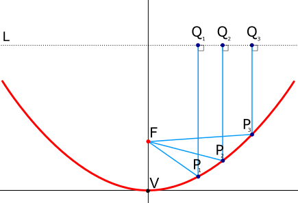
Geometrie des Paraboloids

     Aus dem Bild können wir ersehen, dass die geometrische Länge OP + PQ einen konstanten Wert für das Entwerfen ergibt.

Wir können schreiben, OP + PQ = 2f; 2f ist der konstante Term.

Nehmen wir das an OP = r und so kommt PQ als PQ = r * cosϴ.

Nun ist der Wert von OP + PQ nach dem Ersetzen der Werte,

OP + PQ = r + r * cosϴ = 2f

Oder r (1 + cosϴ) = 2f

Oder r = 2f / (1 + cosϴ) = f * sec2(ϴ / 2)

In der Antennentheorie müssen wir nun die Grundlagen des Koordinatensystems in Form von Sachleistungen halten. Die obige Gleichung kann in rechteckigen Koordinatensystemen unter Verwendung von x`, y`, z` geschrieben werden. Das ergibt die folgende Form.

r + r * cosϴ = √ [(x`) 2 + (y`) 2 + (z`) 2] + z` = 2f

Lassen Sie uns den Einheitsvektor herausfinden, der senkrecht zur Tangente des Reflexionspunktes ist.

f – r * cos2(ϴ / 2) = 0 = S.

Durch einige Rechenoperationen finden wir den Einheitsvektor. Es wird unten beschrieben.

n = N / | N | = – (a) `r cos (ϴ / 2) + – (a) `ϴ Sünde (ϴ / 2)

Mithilfe der geometrischen Analyse können wir nun einen Ausdruck für den Neigungswinkel finden. Es wird unten beschrieben.

tan (ϴ0) = (d / 2) Z.0

Das Z0 ist die Messung der Entfernung von der Achse zum Brennpunkt. Mathematische Ausdrücke können es auch darstellen.

Z0 = f – [(x02 + y02) / 4f]

Oder Z.0 = f – [(d / 2)2/ 4f]

Oder Z.0= f – d2 / 16f

Überprüfen wir den Wert von tan (ϴ0) nach dem Ersetzen des Wertes von Z0.

tan (ϴ0) = [(f / 2d) / {(f / d)2 – (1/16)}]

Entdecken Sie die Anwendungen der Helixantenne! Klick hier!

Richtwirkung der Parabolreflektorantenne

Bevor wir uns mit der Richtwirkung einer Parabolantenne befassen, informieren Sie uns über die Richtwirkung einer Antenne.

Die Richtwirkung einer Antenne ist definiert als das Verhältnis der Strahlungsintensität einer Antenne in einer bestimmten Richtung zur gemittelten Strahlungsintensität über alle Richtungen.

Die Richtwirkung wird als Parameter zur Berechnung der Gütezahl der Antenne betrachtet. Der folgende mathematische Ausdruck beschreibt die Richtwirkung.

D = U / U.0 = 4πU / P.rad

Wenn die Richtung nicht angegeben ist, ist die Standardrichtung die Richtung der maximalen Strahlungsintensität.

Dmax = D0 = U.max / U.0 = 4πUmax / Prad

Hier ist ‘D’ die Richtwirkung und hat keine Richtung, da es sich um ein Verhältnis handelt. U ist die Strahlungsintensität. U.max ist die maximale Strahlungsintensität. U.0 ist die Strahlungsintensität der isotropen Quelle. P.rad ist die gesamte abgestrahlte Leistung. Seine Einheit ist Watt (W).

U = ½ r2 * | E (r, ϴ = π) |2 * √ (ε / μ)

Für U (ϴ = π) und Ersetzen des Energiewerts E wird aus dem vorherigen Wert –

U (ϴ = π) = [16 π2 f2 * Pt * | ∫.0 ϴ tan (ϴ / 2) * √ (G.f (ϴ)) dϴ |2] / 4πλ2

Die Direktivität kommt als – D = U / U.0 = 4πU / P.rad

Oder D = [16 π2 f2 * | ∫.0 ϴ tan (ϴ / 2) * √ (G.f (ϴ)) dϴ |2] /2

Apertureffizienz der Parabolreflektorantenne

1083px Parabolic antennas on a telecommunications tower on Willans Hill

Mikrowellen-Relaisschalen, eine Art Reflektorantenne, Image Credit- BidgeeParabolantennen auf einem Telekommunikationsturm auf Willans HillCC BY-SA 2.5 AU

          Der mathematische Ausdruck für die Parabolreflektorantenne ist unten angegeben.

          εap =s * εt * εp * εx * εb * εr

Hier

εap repräsentiert die Apertureffizienz.

εs ist Spillover-Effizienz. Es kann als der Teil der Leistung definiert werden, der von der Einspeisung übertragen und von der Oberfläche der Reflexion parallel geschaltet wird.

εt repräsentiert die Effizienz der Verjüngung. Es kann als die Singularität der Streuung der Größe für das Feed-Design über die Oberfläche des Reflektors beschrieben werden.

εp gibt uns die Effizienz der Phase. Es kann als die Gleichmäßigkeit der praktischen Feldphase über die Ebene der Apertur beschrieben werden.

εx repräsentiert die Effizienz der Polarisation.

εb ist die Effizienz des Rückstands.

Und εr stellt die Fehlereffizienz dar, berechnet über die gesamte Reflektorfläche.

Mathematisches Problem

1. Eine Parabolreflektorantenne hat einen Durchmesser von 10 Metern. Das f / d-Verhältnis wird mit 0.5 angegeben. Die Betriebsfrequenz ist auf 3 GHz eingestellt. Die Antenne, die mit dem Reflektor gespeist wird, ist symmetrisch aufgebaut. Es ist auch gegeben, dass –

Gf (ϴ) = 6 cos2ϴ; wo ϴo ≤ ϴ ≤ 90o und null an jedem anderen Punkt.

Berechnen Sie nun i) die Apertureffizienz (εap). ii) Richtwirkung der Antenne. iii) Verjüngungseffizienz und Effizienz des Überlaufens. iv) Ermitteln Sie die Richtwirkung der Antenne, wenn die Aperturphasenabweichung auf π / 4 Radian eingestellt ist.

Lösung:

          Wir wissen, dass der Neigungswinkel durch den folgenden Ausdruck gegeben ist.

tan (ϴ0) = [(f / 2d) / {(f / d)2 – (1/16)}]

Oder tan (ϴ0) = [(0.5 · 0.5) / {(0.5 · 0.5) – (1/16)}]

Oder tan (ϴ0) = 0.25 / 0.0625

Oder ϴ0 = 53.13o

Die Apertureffizienz ist gegeben als –

εap = 24 [(Sünde2 (26.57o) + ln {cos (26.57o)}]2 * Kinderbett2(26.57o)

oder εap = 0.75

Der Öffnungswirkungsgrad beträgt also 75%.

Lassen Sie uns nun die Richtwirkung der Antenne herausfinden.

Es kann wie folgt berechnet werden.

D = 0.75 * [π * (100)]2

Oder D = 74022.03

Oder D = 48.69 dB.

Die Überlauffrequenz beträgt εs.

εs = 2 cos3 |0 53.13 / 2 cos3 |0 90 

oder εs = 0.784

Die Spillover-Effizienz der Antenne beträgt also 78.4%.

Jetzt Zeit für die Berechnung der Effizienz des Gewindeschneiders. Die Tapper-Effizienz wird als & epsi; dargestelltt.

εt = (2 · 0.75) / 1.568

oder εt = 0.9566

Der Tapper-Wirkungsgrad für die Parabolreflektorantenne beträgt also 95.66%.

Jetzt wird die Aperturphasenabweichung auf π / 4 Radian eingestellt.

Das heißt m = π / 4 = 0.7854

Wir wissen, dass D / D.0 ≥ [1 – m2/ 2]2

Oder D / D.0 ≥ [1 – (0.7854 * 0.7854) / 2]2

Oder D / D.0 ≥ 0.4782737

Oder D ≥ 0.4782737 * D.0.

Oder D = 0.4782737 * 74022.03

Oder D = 35402.8

Oder D = 45.5 dB.

Die Richtwirkung unter den gegebenen Bedingungen beträgt 45.5 dB.

Helical Antenna: 7 Important Facts You Should Know

Modes

Cover Image Credit – Service Depicted: Air Force
Camera Operator: SSGT LOUIS COMEGER, Hammer Ace SATCOM Antenna, marked as public domain, more details on Wikimedia Commons

Points of Discussions

Introduction to Helical Antenna

            To define a helical antenna, we must know the correct definition of the antenna previously. As per to IEEE standard definitions of antennas or radiators,

“An antenna is a medium for transmitting and receiving radio waves”.

There are several adaptations of antennas. Some of them are – dipole antennas, horn antennas, log-periodic antennas, patch antennas, broadband antennas etc.

Helical Antenna
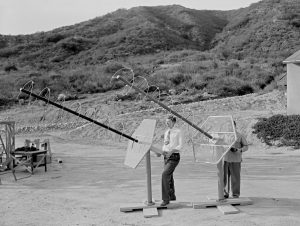
Helical Antenna, Image Credit –
Helical Beam Antennas, 1951” (CC BY-NC-ND 2.0) by NASAJPL

          The helical antennas or helix antennas are one of the categories of broadband antennas. It is one of the most straightforward, primary and realistic antennas with a helical structure, made up of conducting wire-wound.

What is a horn antenna? Explore here!

Geometrical analysis and configuration

          Helical antennas or helix antennas generally come with a ground plane which has the ability to accept distinct forms. To establish a typical helix connection with the ground plane, the ground plane’s diameter should be minimum of 3*λ/4. Although, the plane may be transfused into a cylindrical shaped crater. At the feed point, the transmission lines meet with the antenna.

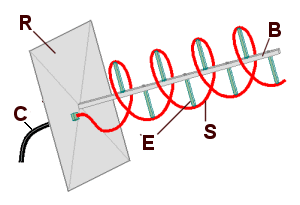
Helical antenna principle
Geometry Of Helical Antenna, Image Credit – UlfbastelHelical antenna principleCC BY-SA 3.0

          The geometrical description of a helix antenna typically consists of N number of turns, the diameter D and the distance between two helical loop S.

The whole length is given by –> L = N S.

The conductive wire’s whole length is given by –> Ln = N L0 (It carries the current primarily obviously!)

 Or, Ln = N √ (C2 + S2); L0 = √ (C2 + S2)

L0 represents the dimension of the wire between two helical loops. It actually gives the length.

C represents the whole circumference of a spiral loop, and it is given by -> π D.

There is another spiral or helix antenna’s parameter, which is also very important. It is represented by the Greek alphabet alpha(α) and termed as ‘pitch angle’. This angle is generally the measurement of the line’s angle – normal to the helix wire and a steep ground to the helix axis. The mathematical expression is given below.

α = tan-1 (S/C)

or, α = tan-1 (S/ π D)

By carefully observing the equation, it can be concluded that when the angle tends to 0 degrees, the winding gets trampled; as a result, the helix antenna gets reduced and becomes similar to a simple loop antenna. Again, when the angle becomes 90 degrees, the antenna becomes a linear wire. When the angle is less than 90 degrees and greater than 0 degrees, then a practical helix has a finite value of circumference.

The architectural parameters can change the radiation properties of the helix antennas. Controlling the geometrical parameters will vary the radiation properties associated with the wavelength. The input impedance has a relation with the pitch angle and conducting wire’s size, as a change in pitch angle values, and the size of the wire will change the input impedance values.

Helical antenna typically shows elliptical polarization, although they can be designed to show circular and linear polarization.

Operational Modes

Helix antennas have the capability to function in many types of operational modes. There are two significant and essential operational modes that we will discuss in detail in the latter part of this article. The two modes are –

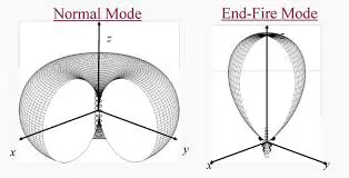
The three-dimensional figures of both the types of mode of operations are given below.

Modes
Radiation pattern of Normal And Axial Mode of helical antenna; Image credit – ocw.ump

As we can see in the standard figure, it has a maximum in an imaginary plane which is normal to the axis, and its null is along the axis. The power pattern has a close similarity to the shape of the circular loop.

Now, the maximum is along the helix’s length for the end-fire mode, and the power pattern is similar to the end-fire array. That is why the mode is named as ‘End Fire Mode’.

The axial mode of operation has more preference over the standard mode of operation because it is more realistic or practical, has better efficiency and can show circular polarization with a broader bandwidth. An elliptically polarized antenna can be described as the summation of the two extraneous lined mechanisms in phase-time quadrature.

What does a transmission line do? Explore!

Normal Mode of Helix Antennas

As discussed previously, the antenna’s helical mode has its maximum radiation is directed to a plane normal to the helix axis, and the null radiation is along its axis. The normal mode of operation of helix antenna or broadside mode operation is achievable by comparing the wavelength, that is N L0 << λ0.

The helix architecture comes down to a loop of a diameter D as the pitch angle comes to 0 to a lined wire with a length of S while approaching to 90 degrees. Nos, as the helix’s geometry, became a loop and a dipole, the far-field radiation in this mode of operation can be represented respectively by Eϕ and Eϴ components of the dipole and the spiral loop.

The helix can be described as N number of small loops and the same number of small dipoles. They are linked with each other in a series manner. The arenas are calculated by using the superposition of the other fields from the rudimentary parts. The loop’s axes and the dipole’s axes coincide with the helix’s axis.

As this model has small dimensions, the current is assumed to be constant. Its operation can be defined by the summation of the fields radiated by a smaller-loops, having a diameter of D and a short dipole having a length of S.

The far-field electric field is given as –

Eϴ = j * η * k * I0 * S * e-jkr Sinϴ / 4πr

The Eϕ part is given by –

Eϕ = η* k2 * (D/2)2 * I0 * e-jkr Sinϴ /4r

The ratio of Eϴ and Eϕ gives the axial ratio. The mathematical expression is given below.

AR = | Eϴ | / | Eϕ |

Or, AR = 4S / πkD2

Or, AR = 2λS/ (πD)2

The pitch angle is given as – α = tan-1 (π D/2λ0)

Axial Mode of operation for Helical Antenna

The axial mode of operation has more preference over the standard mode of operation because it is more realistic or practical, has better efficiency and can show circular polarization with a broader bandwidth.

          This mode is achieved by setting up large S and D. There are some requirements for achieving circular polarization. The range of the circumference of the helix should be in the below-given range.

4/3 > λ0/C > ¾

The pitch angle also has a limited range. The range of the pitch angle is given below.

12o ≤ α ≤ 14o

The terminal impedance range for this mode of operation is between one hundred ohms to two hundred ohms.

The following mathematical operation calculates the gain. For the following equation, S gives the distance between two turns, and N represents the total number of turns in a helical antenna.

G = 15 (C / λ) 2 * (NS / λ)

The half-power bandwidth of helical antenna for this mode of operation is given by following mathematical expression.

HPBW = 52 / [ (C/ λ) * √ {(NS / λ)}]

The full null bandwidth of helical antenna for this mode of operation is given by following mathematical expression.

FNBW = 115 λ3/2 / C * √ (NS)

Check out the radiation pattern of Yagi Uda Antenna!

Helical Antenna Design

  • The input impedance is represented as ‘R’. The mathematical equation for ‘R’ is – R = 140 (C / λ0).
  • The half-power bandwidth of helical antenna for this mode of operation is given by following mathematical expression. It has the accuracy of around plus-minus twenty percent. It is a measurement of angle and has a unit in degrees.

HPBW = 52 λ3/2 / C * √ (NS)

  • The full null bandwidth of helical antenna for this mode of operation is given by following mathematical expression. It represents the measure of beamwidth among the Nulls. It has also unit in degrees.

FNBW = 115 λ3/2 / C * √ (NS)

  • D0 represents the directivity of the antenna. The mathematical equation is –

D0 = 15 * N * C2S / λ03

  • The following mathematical term gives the Axial Ratio or the AR.

AR = 2N+1 / 2N

  • The following expressions give the generalized far-field pattern.

E = sin (π/ 2N) cosϴ sin [ (N/2) * Ψ] / sin (Ψ /2)

Ψ is given by another mathematical equation, and that is further given as Ψ = k0[S * cos ϴ – (L0/p)]

                    The value of ‘p’ for general end-fire array is

p = (L0/ λ0) * (S/ λ0 + 1)

                    The value of ‘p’ for Hansen-woodyard end-fire radiation is

                                        p = (L0/ λ0) * [S/ λ0 + {(2N+1)/2N)}]

Helical Antenna Applications

The helical antenna has several applications in modern communication technologies. It has some unique applications because of its design and radiation patterns. Some of the spiral antenna applications are listed below.

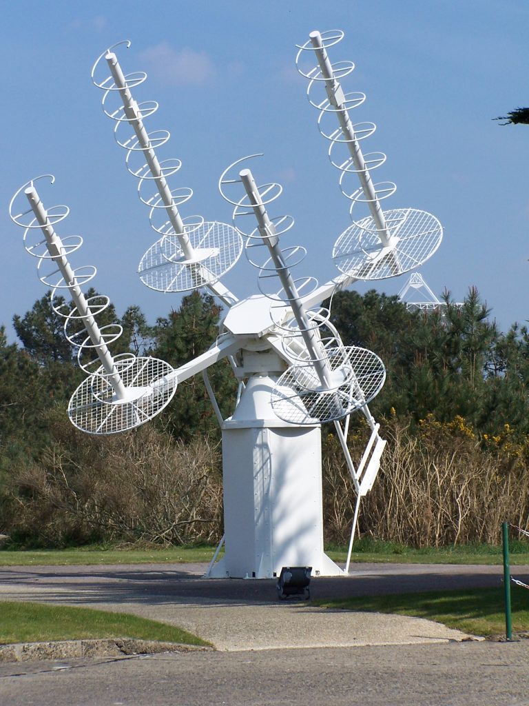
Traqueur acquisition

A satellite tracking helical antenna,

Image credit – KingbastardTraqueur acquisitionCC BY-SA 3.0

  • Helical antennas are efficient in radiating very high-frequency range signals.
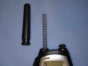
640px UHF CB with rubber ducky exposed
A very common form of helical antenna, Image Credit – Shootthedevgru at English WikipediaUHF CB with rubber ducky exposedCC BY-SA 3.0
  • Helical antennas are often used for space communications and satellites communications.
  • Communications between two planets are possible because of these types of antennas.

Introduction To MOSFET: 11 Important Explanations

MOSFET 1024x748 1 300x219 1

Topic of Discussion: MOSFET basics

What is MOSFET?

Definition of MOSFET:

The Metal-oxide-semiconductor field-effect-transistor (MOSFET), is a form of insulated gate field effect transistor that is made-up by the controllable oxidised silicon based semiconductors”.

Different types of MOS:

  • ·        P Channel MOSFET
  • ·        N Channel MOSFET

Different types of MOSFET devices:

  • ·        Enhancement Mode MOSFET
  • ·        Depletion Mode MOSFET

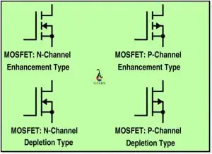
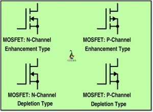
MOSFET Symbol

MOSFET 1024x748 1
MOSFET basics : MOSFET Symbol

Working Principle of MOSFET:

MOSFET Basics

A FET is worked as a conductive  semiconductor channel with 2 contacts – the ‘SOURCE ‘ and the DRAIN. The GATE juntion might be comprehended as a  2 -terminal circuitry as a MOS structure working as a rectifing reverse biasing mode. Usually, the GATE  impedance is higher in classic working situations.

The FETs as per these standards are typically MOSFET, JFET,  metal-semiconductor FET (MESFET), and heterostructure FET. Out of these FET, MOSFET is one of the significant one and commonly utilized for various applications.

In a silicon  based MOSFET, the GATE terminal is normally insulated by a specific SiO2 layer. The charge carriers of the conductive channel develop an opposite charge,  e-  in that case, p-type substrate for an n-channel and ‘holes’ for n-type substrate  for the p-channel. This will induced in the semiconductor at the silicon-insulator edge by the applied volt in GATE terminal. The e- will enter and depart the channel at n+ source and drain terminals cotacts for an n-channel metal-oxide-semiconductor field-effect-transistor.  This will be  p+ contacts during the  p-type Metal-oxide-semiconductor field-effect-transistor.

Mosfet chip
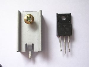
MOSFET basics : A typical MOSFET chip with heat sink
Image credit: WilltronTransistor y disipadorCC BY-SA 3.0

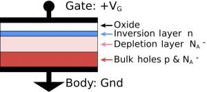
MOSFET layer

MOSFET layer 1
MOSFET basics : MOSFET layers in Metal–oxide–semiconductor structure on p-type silicon Image Credit :MOS_Capacitor.pngBrews ohare derivative work: Fred the Oyster (talk), MOS CapacitorCC BY-SA 3.0

Implementation of MOSFET:

Metal-oxide-semiconductor field-effect-transistors are working as discretized circuit and also as an active element. At the present time, these circuits are scaled down into the deep sub micro meter range. At the moment, the standard 0.13-µicro meter standard technology node CMOS is utilized for VLSI technology and, in future 0.1-µicro meter technology will be existing, with a certain upgradation of speed and integration range.

CMOS technology associates with the n-channel and p-channel Metal-oxide-semiconductor field-effect-transistor to consume very less power without constraining the performing speed. New SOI technology accomplish three dimentional integration with multiple layers, with a electrifying increase in integration stupidity. Novel and enriched structures and the combination of Bi-CMOS technology possibly will lead to further enhancements. One of the emerging areas of CMOS is across a variability of applications from audio device of  kHz range to modern wireless application operated at GHz range.

MOS
MOSFET basics : MOSFET Regions, Image Credit – Cyril BUTTAY, Lateral mosfetCC BY-SA 3.0

Short channel Effect in MOSFET:

Usually FET sizes are assessed by the device aspect ratio. This is the ratio of the gate length in respect of active vertical measurement of FET. The perpendicular dimension for the oxide breadth is measured as parameter di, the source and drain junction depths is considered as parameter rj.  The source and drain junction depletion depths are diefined by the parameter Ws and Wd respectively. The low aspect ratio is identical with short channel characteristics.

                 L<Lmin(µm) = 0.4[rj(µm)di(Å)(Wd + Ws)2(µm2)]1/3

When L is less than Lmin,.

The Metal-oxide-semiconductor field-effect-transistor threshold voltage is consederd as VT . This voltage will be impacted in a number of ways as a result of gate control. Generally, depletion charges near-source and drain are under the common control. The charge will develop a moderately higher portion of the GATE charge carrier. The depletion charge near drain inflates with increasing drain-source biasing voltage, causing in an additional VDS-dependent shift in threshold voltage .

The VT is a sort of barrier combined with carrier injected from the source to channel direction. This barrier is considerably adjusted by use of a drain biasing voltage. In n-channel Field effect transistors, the drain is dropping the threshold voltage and a concurrent rise in the threshold current with growing VDS.

High Field Effect of MOSFET:

In case of drain-source biasing of a Field effect transistor grow towards the drain saturation voltage which termed as ‘VSAT’ wherever a range of higher electric field  is created near by  drain. The  velocity of e-  in that region will saturates. In saturation region, the length considered as ∆L of the high-field  increases in the course of the source with growing VDS, and the performs as if the in effect channel length is decreased  by the parameter ∆L. This phenomenon is entitled as the Channel-length modulation  or  simply termed as CLM in the MOSFET basics. The subsequent simplified manifestation links of VDS to the length of the saturated region is as follows:

                                             VDS = VP + Vα [exp(l/l)-1]]

wherever Vp, Vα, and l are parameters interrelated to the e- saturation velocity. Here, Vp is the potential at the point of saturation in the channel, that is commonly estimated by the parameter VSAT.  Ths agreement is obtained amongst the potential summary which is acquired from the 2D simulation model of an N-channel MOSFET.

Hot Carrier Effects:

Hot-carrier effect is one of  the most important concerns when shrinking FET size into the deep sub micrometre.It decreases the channel length while maintaining high power supply levels. These are increased  to electric field strengths and reasons  of speed up and heating the charged carriers. A comprehensive model for the substrate current is very difficult for circuit-level modelling.

Temperature Dependence and Self-Heating:

The MOSFET basics circuitry is functional in different environs, including different temperatures ranges. Heat created from power dissipation in a circuitry is also significant and the increase in temperature for circuit design is also needed to be considered. The design turns out to be more and more difficult as the device size is becoming very small and power dissipation are increasing with different mode of operation. The thermal characteristics are extensively studied by various models.

For more about MOSFET basics and others electronics related article  click here

CMOS Image Sensor: 5 Complete Quick Facts

Picture1 300x252 1

CONTENTS

  • What is CMOS image sensor ?
  • Different types
  • Working principle
  • Designing
  • Architecture

Cover Image By – Zach DischnerNerd-Tographer Desk Ornament (9698639550)CC BY 2.0

What is CMOS image sensor ?

CMOS Image and Colour Sensor:

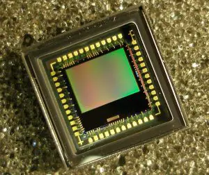
Complementary metal-oxide semiconductor (CMOS) image sensors is comprised of photodiodes with and mixed-signal circuits  ahving capability to amplify small photocurrents into digital signals. The CMOS image sensor is one of the best cricuitry for multiple photography related  applications, i.e digital video cameras, photo scanners, Xerox machine, printing and various others. CMOS are nowadays utilized because of its multiple usage and it’s simple fabrications technique even with constain of sensivity in comparison with CCD.

Three types of the topology of CMOS colour sensors are discussed, namely the transimpedance amplifier (TIA), light to frequency converter, and light integrating.

Picture1
CMOS image sensor
Image Credit : Filya1MatrixwCC BY-SA 3.0

Working Principle of CMOS Image Sensor:

In general, four types of procedures are available

  • Standard CMOS,
  • Analog-mixed-signal CMOS,
  • Digital CMOS, and
  • CMOS image sensor processes.

The most obvious difference between this process and the other processes is the availability of photo devices, such as a pinned photodiode. The advantages of smaller dimension technology are smaller pixel, high spatial resolution, and lower power consumption. A technology lower than 100 nm requires modification to the fabrication process (not following the digital road map) and pixel architecture.

Fundamental parameters such as leakage current (will affect the sensitivity to the light) and operation voltage (will affect dynamic range, i.e., the saturation, a pinned photodiode is most likely not going to work at a low voltage are very important when a process is selected for CIS development. Because of these limitations, a new circuit technique is introduced:

1.  An old circuit, such as a standard pixel circuit cannot be used when using 0.1 micron and lower. This is due to the topology which requires high voltage; because the maximum supply voltage is now lower.

2. Calibration circuit and cancellation circuit are normally employed to reduce noises.

In order to increase the resolution into multi-megapixel and hundreds of frame rate, lower dimension technology is normally chosen. Evidently, it has been reported that 0.13 micron and 0.18 micron are good enough to achieve good imaging performance.

These modifications of the CMOS process have started at 0.25 micron and below to improve their imaging characteristics. As process scaling is going to be much lower than 0.25 micron and below, several fundamental parameters are degraded, namely, photo responsivity and dark current. Therefore, the modifications are focused on mitigating these parameter degradations. System requirements (such as supply voltage and temperature) are also one of the criteria in selecting a suitable process.

The price of tool and development costs will also determine the process selection.

Photo Detetor Devices

The typical photo detector devices are photodiode and phototransistor. Typical photodiode devices are N+/Psub, P+/N_well, N_well/Psub, and P+/N_well/Psub (back-to-back diode) [9]. Phototransistor devices are P+/n_well/Psub (vertical transistor), P+/N_well/P+ (lateral transistor), and N_well/gate (tied phototransistor).

These standard photo devices still require a micro lens and colour filter array. The quantum efficiency of photodiodes in a standard CMOS is usually below 0.3.

The devices which are normally developed for the modified CMOS process are a photogate, pinned photodiode, and amorphous silicon diode. These devices will improve the sensitivity of the CIS. A pinned photodiode, which has a low dark current, offers good imaging characteristics for the CIS.

The photodevices exhibit the parasitic capacitance, which should be considered during the design process. An example of the parasitic capacitance of N_well/Psub is:

                       Cphoto = (capacitance per area) × photodevice area.

Design Methodology of CMOS Image Sensors:

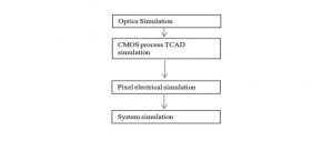
The typical design flow of the CMOS image sensor is shown below.

Typical design flow of the CMOS image sensor

A wave propagation simulation can be done for optics simulation. Commercially available technology computer-aided design tools, such as from Synopsys and Silvaco, can be used to simulate the process or technology of the photodevices. There is a work, (mixed-mode simulation) that combines the technology computer-aided design and pixel-level simulation.

There are many electronic design automation tools available for pixel electrical simulation, these electronic design automation tools are similar to any integrated circuit (IC) design tool, such as spectre, SPICE, Verilog-A, and Verilog. These tools may be time consuming  sometimes if the number of pixels is large.

Indeed, if large pixels together with the deep submicron process are required, more capital has to be provided (cost of tools are more expensive for very deep submicron, especially below 90 nm). Even though the CMOS foundry provides the models for supported design tools, sometimes designers still have to model the sub-block on their own to suit the CIS specification. This can speed up the pixel electrical simulation time, however, this will degrade the accuracy. For system simulation, VHDL-AMS, System-C, or MATLAB can be used to predict the overall function and performance.

CMOS Image Sensor Architecture:

Pixel Level ADC – A digital pixel sensor (DPS) offers a wide dynamic range. The DPS converts the analog values to a digital signa within the pixel range. The processing can also be done at the pixel level.

640px Digital Position Sensitive Device.svg
Digital positive Sensitive device, Image Credit – Georg Wiora (Dr. Schorsch), Digital Position Sensitive DeviceCC BY-SA 3.0

Chip Level ADC – Chip-level ADC or sometimes matrix-level ADC is depicted in Figure below.

chip level
Matrix-level ADC

The ADC for this topology has to be very fast, this topology would also consume a very high current. The ADC type suitable for the CIS topology is pipelined ADC. However, successive approximation register (SAR) and flash type ADC have also been reported in the CIS design. The balance of  necessary overall power intake and speed of operation is therefore essential.

Digital Pixel Sensor – The DPS concept is similar to the solution used in the CMOS neuron-stimulus chip. The DPS in number is found useful for on-chip compression. The photodiode is used to discharge the input capacitance of the comparator and photodiode itself. It will be discharged proportionally to the light intensity. When this reaches the threshold, the   comparator’s O/P will be triggered.

Low Power Technique in CMOS Image Sensor:

Biasing method: The subthreshold region or weak inversion biasing is one of the approaches to achieve low current consumption. This technique can be applied to an operational transconductance amplifier (OTA) or an amplifier for an ADC. Triode region biasing can also be used to further reduce power consumption.

Circuit technique: The regenerative latch can be used to reduce the digital power consumption. Reducing/scaling the capacitors in the pipeline stages (for ADC) can also reduce the power consumption.

Advanced power management technique: Another type of biasing or circuit technique, a “smart” approach, such as harvesting solar energy can also be employed to reduce the power consumption. We can also selectively ON only the required readout circuit. Pixels can also be periodically activated to reduce the power consumption further.

Low Noise Techniques in CMOS Image Sensor:

At pixel level: The thermal noise can be reduced by correlated double sampling and oversampling. The flicker noise is reduced by using a large device, periodically biasing the transistor, and proper PMOS substrate voltage biasing.

Column level: The off-chip calibration can be used to reduce fixed pattern noise. The calibration is done to select suitable capacitor weights in the SAR ADC.

ADC level: The kT/C noise is reduced by selecting a suitable value for Cf and Cs of the S/H circuit and buffer.

Photodiode level: The high conversion gain helps to reduce referred-to input noise.

For more electronics related article click here

What Is Yagi Uda Antenna: 7 Answers You Should Know

Drawing of Yagi Uda

Image Credit : Raysonho @ Open Grid Scheduler / Grid EngineYagiAntennaCC0 1.0

Points for Discussion

  • Introduction
  • Use of Yagi uda antenna
  • Elements of a typical Yagi Uda antenna
  • Yagi uda antenna construction
  • Yagi Uda Antenna Design
  • Yagi uda antenna radiation pattern
  • Few mathematical problems related to Yagi-Uda antenna

Introduction

To define a Yagi-Uda antenna, we should know the proper definition of the antenna. According to IEEE standard definitions of antennas, “An antenna is a means for radiating or receiving radio waves”.

A yagi-uda antenna is basically an array of rectilinear dipoles with a feed element and other parasitic elements. It can be described as an end-fire array which means the array is set of internally connected antennas and the total unit functions as a single antenna.

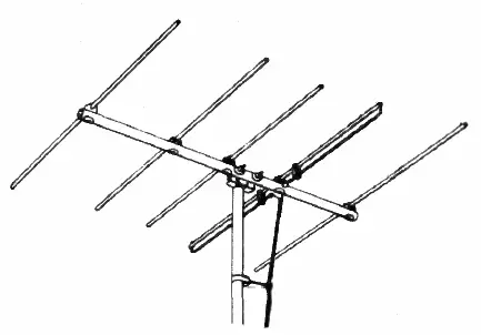
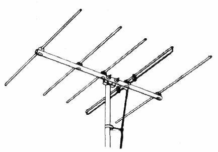
Yagi Uda Antenna

Drawing of a typical Yagi Antenna,

Image Credit- Unknown authorUnknown author, Yagi TV antenna 1954, marked as public domain, more details on Wikimedia Commons

Yagi Uda antenna is a very realistic antenna for the high-frequency domain as it operates in the high-frequency field to an ultra-high frequency domain.

Professor S. Uda and professor H. Yagi of Tohoku Imperial University, Japan, first described this type of antenna’s operation. The antenna is often interrupted as ‘Yagi Antenna’.

What is horn Antenna? Check out here!

Use of yagi uda antenna || Applications of yagi uda antenna

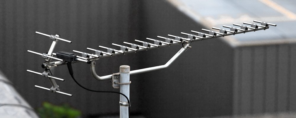
            Yagi antenna is one of the widely used antennae. It has been used as TV antennas at uncountable homes due to its high directivity. Many readers would recognize it just seeing the picture. It has application in amateur radios, in fields of RADARs, in satellites and RFID applications.

UHF TV Antenna 001

A modern High Frequency yagi-Uda antenna, used for television,

Image Source – Tennen-GasUHF TV Antenna 001CC BY-SA 3.0

Elements of a typical Yagi Uda antenna

As earlier said, a typical Yagi Uda antenna, is an array of small antennas and it has one element for energy feed and others are parasitic.

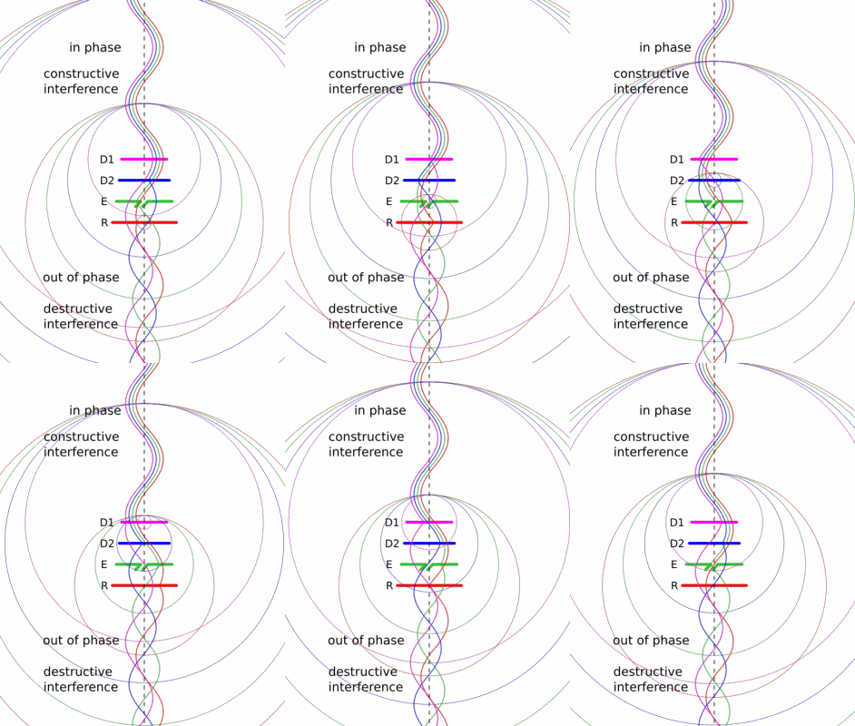
The most used feed element of a yagi uda antenna is a folded dipole. The radiator is specially constructed for operation of an end-fire array. Parasitic elements at the forward beam act as directors and the pieces at the rear beam act as reflectors. This completes the antenna.

The thin rods are aligned on a crossbar with their centres. There is one driven element, several parasitic elements, a reflector, and one or more directors. As the name suggests, the parasitic elements are not physically connected with the transceiver and work as passive radiators. They radiate radio waves which further affects the radiation pattern. The distance between the two rods depends on the wavelength of the signal. Typically, the distance changes from one-tenth to one-fourth of the wavelength.

The directors’ size is generally shorter than the driven element, which is also more concise than the reflector.

The gain of a yagi uda antenna depends upon the number of parasitic elements present. Increase in the number of parasitic elements increases the overall gain of the antenna. That is why there are numerous directors in a yagi-uda antenna. As the reflector has a negligible effect on the antenna gain, there is only one reflector in the antenna.

Yagi uda antenna construction

We will discuss the construction of a few parts of the yagi uda antenna. The stakes are – Driven element, Director, & the Reflector.

  • Director: It is the shortest element of the yagi uda antenna. This part is directed towards the receiving source. The length of the detectors depends upon the distance between the details and the wavelength of the signals. The gain of a yagi uda antenna has a relation with the length of the antenna. The antenna length also increases by increasing the number of directors.
  • Driven element: It is the element which has the feed point for energy. The transmitter is connected with this element through the feed point. The feed point typically lies at the centre of the component. The length of the part is half of the wavelength.
  • Reflectors: It is a single unit and constructed at the end of the antenna array just after the driven element. It has the highest length among the parasitic elements. The spacing of reflector depends on the wavelength, beamwidth and gain of the yagi uda antenna. The resonant frequency of reflector is generally lower.

How transmission lines are related with antennas? To know – click here!

Working of yagi uda antenna

Let us draw some attention towards the operation and working of a yagi uda antenna. Assume a typical yagi uda antenna with a reflector, with a driven element and a single director.

As discussed earlier, the driving element’s length is half of the dipole, and it is connected with electrical energy directly. It supplies power throughout the antenna as it has the feed point, and all other parasitic elements are internally associated with this element.

Now, assume the parasitic elements (both the reflectors and directors) as a general dipole element of a measurable diameter and fed at the middle via a short circuit. Transmission line theory says that a short circuit is enabled to reflect power at 180 degrees.

330px Yagi 3 element.svg

Parts of a typical yagi-uda antenna,

A – Driven Element, R – Reflector, D – Director,

Image Credit – SankeytmYagi 3 elementCC BY-SA 3.0

Thus, the operation can be designed as the mixing up of a power receiver dipole element that receives the power and sends to the matched load and a power transmitter dipole element that transmits the power to the array of the antenna.

Now, at an instant, if the received and sent power are in 180 degrees out of phase with each other, then the result will be zero voltage. That signifies the short circuit of the diode at the feed point. That is why the radiated power is in 180 degrees phase out with the incident waves.

The parasitic elements in the antenna are shorter than ½λ. The reflector is longer than ½λ, and it generally lags the phase of open-circuit voltage. The incoming signal generates the voltage. The director is also shorter than ½λ. It lags the voltage that of current.

Yagi Uda antenna design

Unlike the horn antenna, there are no hard and fast rules to design a yagi-uda antenna. There are some critical physical parameters which resist doing so. Some of the parameters are as follow –

  • ‘Length of element and distance between them.’
  • The measurement of the rods or the diameter of the rods.
  • Some critical parameters like – Gain and input resistance.

Though, there are some methods for analysis and calculation to find out the desired results. For an n-element yagi uda antenna, there are 2n-1 numbers of parameters to consider.

The analysis for current distribution is done by solving the ‘Hallen’s integral equation’. The assumption of a classical standing wave and condition of other conductors are also taken into account. The analysis method is complicated and requires accurate results though some vital approximations are necessary to complete it.

The designed antennas go through trial-and-error methods to modify further. Sometimes, the antenna starts with a design and ends up with another after certain modifications in the process. Nowadays, computer simulation helps designers/ engineers to check the result.

Yagi Uda antenna radiation pattern

Radiation Pattern is the angular dependence of the strength of the radio waves from any electromagnetic source. The below image shows the radiation pattern of a yagi uda antenna.

Yagi antenna animation 16 frame 1.6s
Yagi uda antenna radiation pattern, Image By – ChetvornoYagi antenna animation 16 frame 1.6sCC0 1.0

Advantages yagi uda Antenna || Disadvantages of yagi uda antenna

            Yagi uda antenna has both its advantages and disadvantages. But there is no doubt that this antenna has made some drastic changes in the field of commercial antennas. It has the highest ever popularity as TV antennas because of its large bandwidth. Let us discuss some of its advantages.

Advantages of yagi uda antenna

  • Yagi uda antenna has a decent gain of 7dB, which is sufficient for its applications.
  • Yagi uda antenna array is direction type of antenna.
  • This type of antennas is suitable for applications in high frequency to the ultra-high frequency range.
  • These antennas have adjustable from to ack ratio.

Let us discuss some drawbacks of yagi uda antenna.

Disadvantages of yagi uda antenna

  • Though the applications of yagi uda antennas are suitable for the antenna’s gain, the gain is not very high compared to any other types of antenna.
  • The designing has a requirement of a large number of elements.
  • Any damage to the parasitic elements leads to the dysfunctionality of the whole antenna.
  • The size is quite large, that is why nowadays the antennas are not used by peoples.

Few mathematical problems related to Yagi Uda Antenna

1. Design a yagi uda antenna with the following specifications. Directivity: Relative to ½λ dipole and situated at the same level. Magnitude: 9.2 dB. f0 = 50.1 MHz. The desired diameter of the parasitic rods: 2.54 cm. The desired diameter of the metal supporting boom: 5.1 cm. Find out the spacings between elements, lengths and length of the entire array.

Solution:

            The operating frequency is given as 50.1 MHz. The wavelength comes as λ = 5.988m.

The desired diameter of the parasitic rods is given as d = 2.54 cm.

Therefore, d /λ = 2.54/598.8

Or, d /λ = 4.24 x 10⁻³ 

The desired diameter of the metal supporting boom is given as D = 5.1cm.

Therefore, D /λ = 5.1 / 598.8

Or, D /λ = 8.52 x 10⁻³

            We need to use a chart that gives us ‘optimized uncompressed lengths of parasitic elements of a yagi-uda antenna’. Using this chart, we can understand that the desired antenna array would have a total of five elements (one driven element, one reflector and three directors).

The second column of the chart gives us the optimum uncompressed length for the value of d/λ = 0.0085.

l1 = 0.482λ

l3 = 0.428λ

l4 = 0.424λ

l5 = 0.428λ

The overall antenna length will be L = (0.6 + 0.2) λ = 0.8λ. The spacing or the distance between the directors parasitic will be 0.2λ and the spacing of the reflector will be same that is 0.2λ.

What Is Horn Antenna: 9 Important Concepts

ATM Horn Antennas 300x228 1

Image Credit: Schwarzbeck Mess-Elektronik, Schwarzbeck BBHA 9120 DCC BY-SA 3.0

Points for Discussion: Horn Antenna

  • Introduction
  • Use of horn antenna
  • Elements of a horn antenna and Types of horn antenna
  • Horn antenna design
  • Directivity of horn antenna
  • Horn antenna radiation pattern
  • Horn antenna gain
  • Horn antenna beamwidth
  • Few mathematical problems related to Horn Antenna

Introduction

To define a horn antenna, we should know the proper definition of the antenna. According to IEEE standard definitions of antennas,

“An antenna is a means for radiating or receiving radio waves”.

Horn antenna is the most popular type of Aperture antenna. Aperture antennas are specially designed for microwave frequencies. These types of aperture antennas are widely used and most unadorned other than any kinds.

Though horn antenna usage was started back in the 1800s, the rapid application was created in the 1930s. These antennas had also undergone drastic modification during this time. Numerous thesis and research were done to describe the horn-antenna’s design, find out the radiation pattern of horn-antenna, and applications in different sectors. The applications in microwave and waveguide transmission domain made horns antenna famous. That is why horn- antennas are often interpreted as a microwave horn-antenna.

What is Transmission Line? How it is related to antenna? Know here!

Use of Horn Antenna

Horn-antennas have found impactful applications as feed elements for hefty radio astronomy, satellite tracking, communication dishes, and many other places. It is used as a feed for reflector and lenses and also used in phased arrays. These antennas are preferred over different types of aperture antennas, because of its fair and straightforward design, better gain, versatility, and overall performance.

Elements of a horn antenna

Horn antenna is a resonating pipe of various designs which can be shaped for making a larger opening. The overall performance of the antenna is affected by the direction, taper’s amount, directivity.

Types of horn antenna

Horn-antennas have different forms for operations. They are –

·       Sectoral Horn Antenna

  • E-Plane
  • H-Plane

·       Pyramidal Horn Antenna

ATM Horn Antennas
A typical pyramidal horn -antenna, Credit – Tactron ElektronikATM Horn AntennasCC BY-SA 3.0

·       Conical Horn Antenna

BocinaLenteDielectrica
Conical Horn -Antenna and its radiation pattern; Image Credit – Mª Luisa BelloBocinaLenteDieléctricaCC BY-SA 4.0

·       Corrugated horn antenna

640px LNB 2
Corrugated horn- antenna; Image Credit: Laurent06LNB 2CC BY-SA 3.0

·       Diagonal horn antenna

NRAO Calibration Horn Antenna 1967
Diagonal Horn Antenna; Image Source – NRAO/AUI/NSF, NRAO Calibration Horn Antenna (1967)CC BY 3.0

·       Ridged horn antenna

640px Schwarzbeck BBHA 9120 D 1
Ridged horn Antenna; Image Credit –Schwarzbeck Mess-Elektronik, Schwarzbeck BBHA 9120 DCC BY-SA 3.0

·       Dual-mode conical horn antenna

·       Septum horn antenna

·       Aperture-limited horn antenna

Horn antenna design (Pyramidal Horn Antenna)

Pyramidal horn-antenna is the most used and popular types of the horn-antenna. It is known as a standard gain horn (that is why we choose pyramidal horn for describing). The pyramidal horn’s radiation pattern is the combination of E- and H- sectoral horn-antennas. Let us discuss the design of a pyramidal horn-antenna.

Design Procedure

  • The designer/ engineer should know the gain (G0). Also the measurements of ‘a’, ‘b’, of the quadrilateral waveguide (used as feed) should be known.  
  • The designing aims to derive dimensions such as – a1, b1, ρe, ρh, Pe, Ph. The calculation should lead the designer to the optimum gain of the horn- antenna.
  • The selection of a1 and b1 should also be in a guided way so that they will help to find the optimum gain, and we can derive the design equations.
  • The efficiency of a horn- antenna including the apertures is about 50%. Now, we know that –

a1 ≈ √ (3λρ2)

b1 ≈ √ (2λρ1)

The directivity is given as – D0

D0 = Aem [ 4π / λ2]

Aem is the maximum effective area and has a relationship with the physical area (abbreviated as Ap).

Aem = εap Ap

εap is the aperture efficiency, 0 ≤ εap ≤ 1

Gain = G0

G0 = (1/2) * (4π / λ2) * (a1 b1)

Or, G0 = (2π / λ2) * √ (3λρ2) * √ (2λρ1)

Or, G0 (2π / λ2) * √ (3λρh * 2λρe) — (1)

As we assume ρ2 ≈ ρh and ρ1 ≈ ρe for long horn-antennas.

Now, to realize the physical horn- antenna, Pe and Ph must be equal.

We know that,

Pe = (b1 – b) [ (ρe / b1)2 – ¼]1/2

Ph = (a1 – a) [ (ρh / a1)2 – ¼]1/2

Now, we can rewrite the equation (1) as below.

[√ (2χ) – b/ λ]2 (2χ -1) = [{(G0 /2π√χ) * √ (3/2π)} – (a/ λ)]2 * [(G02 / 6π3χ) – 1] — (2)

Where,

ρe / λ = χ and,

ρh / λ = G02 / 8π3χ

Equation (2) is known as the horn- antenna design equation.

  1. At first, we have to calculate the value of χ, which will gratify the value of gain. An iterative approach with a trial value is considered to find out the value χ.

χ (trail) = χ1 = G0 /2π√2π

  1. Once the correct value is calculated, the value of ρe and ρh are calculated.
  2. The a1 and b1 related to the designs are calculated after that.

a1 = √ (3λρ2) ≈ √ (3λρh) = (G0 /2π) * √ (3λ/2πχ)

b1 = √ (2λρ1) ≈ √ (2λρe) = √ (2λχ)

  1. The values of pe and ph are calculated at last.

Directivity of Horn Antenna

Before we step into finding out the directivity of a horn-antenna, let us know the directivity of an antenna? An antenna’s directivity is defined as the ratio of radiation intensity of an antenna in a particular direction to the averaged radiation intensity over all the directions. Directivity is considered as a parameter for calculating the figure of merit of the antenna.

The following mathematical expression describes the directivity.

D = U / U0 = 4πU / Prad

When the direction is not given, the default direction is the direction of maximum radiation intensity.

Dmax = D0 = Umax / U0 = 4πUmax / Prad

Here, ‘D’ is the directivity, and it has no direction as it is a ratio. U is the radiation intensity. Umax is the maximum radiation intensity. U0 is the radiation intensity of the isotropic source. Prad is the total radiated power. Its unit is Watt (W).

As earlier said, the horn-antenna is of three types. All the classes have different directivity. Let us discuss all of them.

E-Plane Sectoral Horn

The following expression gives the directivity of the E-Plane horn-antenna.

DE = 4πUmax /Prad = (64aρ1 * | F(t) | 2)/πλ b1

Where, | F(t) | = [C2b1 / √ (2λρ1) + S2b1 / √ (2λρ1)]

H-Plane Sectoral Horn

The following expression gives the directivity of the H-plane sectoral horn-antenna.

DH = 4πUmax /Prad = [4πbρ2 /a1 λ]* {[ C(u) – C(v)]2 + [S(u) – S(v)]2}

Where,

u = (1/√2) * [{√ (λρ2)/a1 + a1/ √ (λρ2)}]

v = (1/√2) * [{√ (λρ2)/a1 – a1/ √ (λρ2)}]

Pyramidal Horn Antenna

The directivity of pyramidal horn- antenna depends on both the directivity of E & H plane sectoral horn. The equation is given below.

DP = 4πUmax /Prad = [8πρ1ρ2 /a1b1] * {[ C(u) – C(v)]2 + [S(u) – S(v)]2} * {[C2b1 / √ (2λρ1) + S2b1 / √ (2λρ1)]}

It can be written as –

DP = [π λ2 / 32ab] * DEDH

Horn Antenna Radiation Pattern

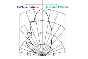
Radiation Pattern is the angular dependence of the strength of the radio waves from any electromagnetic source. The below image shows the radiation pattern of a pyramidal horn-antenna.

Pyramidal Horn Antenna Radiation Patterns 1

Image depicting Horn antenna radiation pattern

Horn Antenna Gain

An antenna’s gain would refer to as the ratio of the intensity in a particular direction to the radiation intensity if the antenna were radiated isotopically. It is an essential parameter for measuring an antenna’s performance and has a close relationship with the antenna’s directivity. The gain of a horn- antenna lies around 25 dBi and the range is typically 10 – 20 dBi.

Horn antenna beamwidth

Antenna bandwidth is the angular distance between two matching points on the reverse side of the outline supreme. The horn-antenna beamwidth gets decreased if the frequency of the process gets increased.
The bandwidth of a practical horn-antenna stays in a range of 10:1 to 20:1.

Few mathematical problems related to Horn Antenna

1. Find the directivity of the E-plane sectoral horn-antenna. The details for the antenna are given below. a = 0.5λ, b = 0.25λ, b1 = 6λ, ρ1 = 6λ

Solution:

b1 / √ (2λρ1) = 6λ / √ (2λ*6λ) = 6 / √12 = 1.73

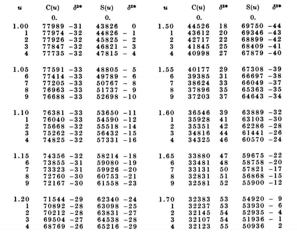
Frensel 1 1

A part of Fresnel Integral Chart; Image Credit – A. VAN WIJNGAARDEN and W. L. SCHEEN

Now, [C (1.73)]2 = (0.32)2 = 0.1024 [from the chart of Fresnel integrals]

And, [S (1.73)]2 = (0.54)2 = 0.2916 [from the chart of Fresnel integrals]

We know that, DE = 4πUmax /Prad = (64aρ1 * | F(t) | 2)/πλb1

Where, | F(t) | = [C2b1 / √ (2λρ1) + S2b1 / √ (2λρ1)]

DE = [{64 (0.5) * 6 * (0.1024 + 0.2916)} / 6π]

Or, DE = 4.01 dB.

So, the directivity of the given E-Plane Sectoral Horn-Antenna is 4.01 dB.

2. Find the directivity of the H-plane sectoral horn-antenna. The details of the antenna are given below. a = 0.5λ, b = 0.25λ, a1 = 6λ, ρ2 = 6λ

Solution:

We know that,

u = (1/√2) * [{√ (λρ2)/a1 + a1/ √ (λρ2)}]

v = (1/√2) * [{√ (λρ2)/a1 – a1/ √ (λρ2)}]

Now, u = (1/√2) * [{√ (6)/6 + 6/ √ (6)}] = 2.02

And, v = (1/√2) * [{√ (6)/6 – 6/ √ (6)}] = – 1.44

Using Fresnel integrals,

C (u) = C (2.02) = 0.48825

C (v) = C (-1.44) = -C (1.44) = – 0.54310

S (u) = S (2.02) = 0.3434

S (v) = S (-1.44) = -S (1.44) = – 0.71353

We know that directivity of H-plane sectoral horn- antenna is 

DH = 4πUmax /Prad = [4πbρ2 /a1 λ]* {[C(u) – C(v)]2 + [S(u) – S(v)]2}

Or, DH = [4π (0.25)6/6] * [ (0.488 + 0.543)2 + (0.343 + 0.713)2]

Or, DH = (3.141) * (1.0629 + 1.1151)

Or, DH = 6.84 dB

So, the directivity of the given H-plane Sectoral Horn-Antenna is 6.84 dB.

3. Designing details of a pyramidal horn-antenna is given below. ρ2 = 6λ = ρ1 = 6λ; a = 0.5λ, b = 0.25λ; a1 = 6λ = b1 = 6λ; Check if a practical horn-antenna can be designed with those details. Also, find out the directivity of the pyramidal horn- antenna.

Solution:

            Now, ρe = λ √ ([62+ (6 / 2)2] = 6.708λ

            And, ρh = λ √ ([62+ (6 / 2)2] = 6.708λ

We know that,

Pe = (b1 – b) [ (ρe / b1)2 – ¼]1/2

Ph = (a1 – a) [ (ρh / a1)2 – ¼]1/2

Now, Pe = (6λ– 0.25λ) [ (6.708 / 6)2 – ¼]1/2 = 5.74λ

And, Ph = (6λ– 0.5λ) [ (6.708 / 6)2 – ¼]1/2 = 5.12λ

As we can see, Pe is not equal to Ph, so the design is not possible to implement.

            We know that the directivity of a pyramidal horn-antenna is 

DP = [π λ2 / 32ab] * DEDH

            Now, DP = [π / 32 * (0.5) * (0.25)] * 6.84 * 4.01]

            [The value of DEDH is has been calculated previously]

            Or, DP = 21.54

            Converting it to the dB value, DP = 10log21.54 = 13.33 dB

So, the directivity of the given Pyramidal Horn-antenna is 13.33 dB.

Transmission Line: 5 Facts You Should Know

TINE

Cover Image Credit – Sajad-HasanAhmadiTV antenna connectorsCC BY-SA 4.0

Points of Discussion: Transmission Line

  • Introduction
  • Purpose of transmission line
  • Analysis of transmission line
  • Types of transmission line
  • Applications of transmission lines

Introduction to Transmission Line

A transmission line is a specially designed cable for transmission of power. It conducts only electromagnetic waves to the load at low frequencies in a guided way.

            Transmission line operates at microwave frequency domain and radio frequency domain where power is assumed as an electromagnetic wave. That is why if any cable can guide an electromagnet signal, then it will be called a Transmission line.

            The transmission line is the result of researches of James Maxwell, Lord Kelvin, and Oliver Heaviside. The fault and drawbacks of the ‘Atlantic telegraph cable’ and invention of telegrapher’s equation made the way out for the line.

Purpose of transmission line

Regular cables which transfer electrical energy are designed to conduct power at lower frequency AC. They cannot carry power in FR range or above 30 kilo hertz as the energy gets disconnected at joints and connectors, and some time does not reach the destination. This lines resolve these problems. They are constructed specially to minimize the reflections and loss of power and also uses the impedance matching to carry power.

            This lines are constructed with a uniform cross-sectional area. That is why they provide uniform impedance which is in terms known as characteristic impedance.

Transmission Line

Use of Transmission Line in antenna

            The wavelength of the electromagnetic waves gets shorter as the frequency gets higher of the electromagnetic waves.  Transmission lines are crucial because when the wavelength is short enough, the length of the wire contributes to the past of the wavelength.

What is a Yagi Uda Antenna? Click here for details!

Analysis of Transmission line

            We assume a four-terminal model of the transmission lines to analyze the construction and working of lines. It is equivalent to a typical two-port circuit. 

            We assume that the circuit is linear, which means that the complex voltage at any port is relational to the complex current for the reflectionless condition. Also, we assume that two of its ports are transposable.

Characteristics impedance of transmission line

Characteristic impedance or (Z0) is an essential parameter of the line. It can be defined as the ratio of the magnitude of the voltage to the magnitude of the current of a wave, travelling along a reflection less line.

Characteristics impedance controls the behaviors of the line only if the line is uniform in length. Generally, for co-axial cables, characteristic impedance has a value of fifty to seventy ohms, and for warped pair of wires, the value is 100 ohms. For untwisted pair, the value is 300 ohms.

Transmission line reflection coefficient

The line’s reflection coefficient is given by the ratio of the complex magnitude of the reflected signal to the incoming signal. It is represented by the Greek alphabet – Г and expressed as –

Transmission line reflection coefficient

where V+ is the complex voltage of the incoming voltage and  V- is the complex voltage of the reflected wave.

It has a relation with the load impedance and characteristic impedance. The expression is given below.

Transmission line

Here ZL is the load impedance, and Z0 is the characteristic impedance.

The standing wave ratio also has a relation with this line reflection coefficient. The connection is given as –

Transmission line

The relation between Standing Wave Ratio and transmission line reflection coefficient.

Matched condition of transmission line:

The aim of a transmission line is to deliver the maximum power from the source to destination load and to minimize the reflection and loss of the power. The ‘matched’ condition can fulfil this desired. If the destination’s load impedance is made same or equal to the value of the characteristic impedance of the line, then the line achieves ‘matched’ condition.
            Instead of the ‘matched’ condition, the transmission suffers some loss. Like, ohmic loss. There is also another substantial loss that occurs when this line works in high frequency ranges. The loss is known as dielectric loss. Here, the inside elements of this lines, grips the EM energy and produces heat.

            The aggregate loss of this line is measured by the unit dB/m. The losses are dependent on the frequency of the signal, as mentioned earlier. The constructor companies of this usually provide a chart of loss. It shows the loss of power at different frequencies. If any line suffers a loss of three decibel/meter, then the power received at the load will be half of the power supplied.
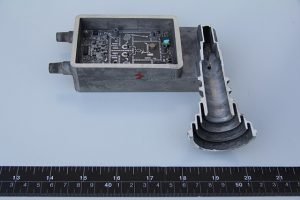
What is horn antenna? get an overview here!

Types of transmission lines

 These come with certain types depending upon its physical structure and according to the needs. Some of the essential and widely used types of transmission lines are listed below. Please go through it and discover them.
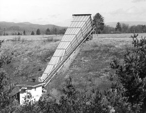
Co-axial cables:

It is one of the widely used forms of lines. It restricts the whole EM wave inside the cable. Thus, co-axial cables can be bent, strapped as well as twisted to an extent without affecting the operation.

Co axial cable

Cross-section of a Co-axial Cables, Image Credit: Tkgd2007Coaxial cable cutawayCC BY 3.0

EM waves promulgate in TEM or transverse electric and magnetic mode For the RF range applications. Here, both the electric and magnetic fields are perpendicular with the promulgate directions. The electric field becomes radiated, and the magnetic field becomes circumferential.

If the wavelength of the wave is shorter than the circumference of the co-axial cable, then the TEM gets divided into two. The modes are then known as TE or transverse electric and TM or transverse magnetic.

Co-axial cables have broad applications for televisions. It was primarily used for telephones in the middle of twenty century.

Microstrip transmission lines:

A microstrip network is basically a tiny conductive plane, placed parallelly to the ground surface. It can be designed by putting a thin and flat metallic plane on the side of a PCB. The opposite surface must be the ground plane. The characteristic impedance of the microstrip type line depends on that conductive strip. The height, width, dielectric coefficient of the conductive strip provides the characteristic impedance. A point to be remembered that the microstrip type line is an open structure while the co-axial cable is a closed one.

640px Electric and Magnetic Fields for Microstrip.svg

Electric & Magnetic field of Microstrip Transmission Line,

Image Credit: Dassault

Twisted pair transmission lines:

In this type of line where pairs of wire are assembled together to form a single chain or a cable is known as tangled pair transmission lines. These types of lines are used in global telephonic communications. Also, it has used in data circulation inside buildings. This type is not economical due to its properties.

640px Twisted pair.svg

Image of a Twisted Pair types. Image Credit – Spinningspark at en.wikipediaTwisted pairCC BY-SA 3.0

Star quad:

Star quad is another wire-combinational formation. It uses four cables, and all the conductors of the four cables are twisted and assembled along the axis of the cable. In this formation, each and every pairs uses a far pair to get connected.

The combinational form of twisted, balancing and quadrupole pattern of transmission lines has several benefits as it reduces noise, particularly for short signal level usage like – cables of the microphone.

Transmission line

Descriptive image of a star quad cable, Image Source – Spinningspark at en.wikipediaDM quadCC BY-SA 3.0

This type of line has applications in four-wire telephony, two-wire applications.

It also induces high capacitance which further causes distortion and losses.

Applications of transmission lines | Uses of transmission lines

Transmission lines have several benefits over regular electrical cables in specific domains. That is why it has several applications. Let us discuss some of them.

  • Electromagnetic powers are supplied in high frequency domains with minimum loss. Tv and radio cables for connecting the aerials is one of the most famous examples.
  • These are also used for the generation of pulses by charging and discharging this lines. A significant example of this type of line is – Blumlein Transmission Line. Radars have also multiple application of this kind.
  • These are also applied in stub filters. Stub filters are typically wired in a parallel connection and transfer power from the source to destinations.

Check out more on Electronics! Click Here!