Astable And Bistable Multivibrator:7 Facts You Should Know

image001 6

In this article we will study about the Schmitt trigger Comparator and Oscillator circuitry with different related parameters in detail. As we have seen till now that an op-amp is used in various fields of applications and being such a versatile device its importance as a part of analog circuits is immense. One of the most convenient applications of the op-amp is as a multivibrator circuit. We will be studying in detail about types and working of multivibrator circuit constructed using op-amps (op-amp multivibrators) and other passive devices such as capacitors, diodes, resistors etc.

Contents

  • Introduction of Multivibrators
  • Positive feedback usage in multivibrator
  • What is Schmitt trigger ?
  • Schmitt trigger comparator closed-loop circuit or bistable multivibrator
  • Voltage transfer characteristics of Bistable multivibrator
  • Astable multivibrator or Schmitt trigger oscillator
  • Oscillator’s duty cycle

Introduction of Multivibrator and Schmitt trigger Circuitry

Multivibrator circuits are sequential logic circuits and are of many types depending on how they are created. Some multivibrators can be made using transistors and logic gates, whereas there are even dedicated chips available as multivibrators such as NE555 timer. The op-amp multivibrator circuit has a few advantages over other multivibrator circuits as they require much fewer components for their working, less biasing, and produces better symmetrical rectangular wave signals using comparatively fewer components.

Types of Multivibrators

There are mainly three types of multivibrator circuits present:

  1. Astable multivibrator,
  2. Monostable multivibrator
  3. Bistable multivibrator.

The monostable multivibrator has single stable state, whereas the number of stable-states a bistable multivibrator has- is 2.

As we have learnt in the previous section about op-amp as a comparator, in the open-loop configuration the comparator can switch in an out of control manner between the positive saturation supply rail voltage and negative saturation supply rail voltage when an input voltage near to that of the reference voltage is applied. Hence, to have control on this uncontrollable switching between the two states, the op-amp is used in a feedback configuration (closed-loop circuit) which is particularly known as closed-loop Schmitt trigger circuit or bistable multivibrator.

Positive feedback usage in multivibrator and hysteresis effect

Till now, we have learnt about the negative feedback configuration in op-amps in the previous sections. There is also another type of feedback configuration known as positive feedback, which is also used for specific applications. In positive feedback configuration, the output voltage is fed back (connected) to the non-inverting (positive) input terminal unlike the negative feedback, where the output voltage was connected to the inverting (negative) input terminal.

An op-amp operated in a positive feedback configuration tends to stay in that particular output state in which it is present, i.e. either the saturated positive or saturated negative state. Technically, this latching behaviour in one of the two states is known as hysteresis.

If the input applied signal in the comparator consists of some additional harmonics or spikes (noise), then the output of the comparator might switch to the two saturated states unexpectedly and uncontrollably. In this case, we won’t get a regular symmetrical square wave output of the applied input sinusoidal waveform.

But if we add some positive feedback to the comparator input signal, i.e. use the comparator in a positive feedback configuration; we will be introducing a latching behaviour in the states, what we technically call as hysteresis into the output. Until and unless there is a major change in the magnitude of the input AC (sinusoidal) voltage signal, the hysteresis effect will continue to make the output of the circuit remain in its current state.

What is Schmitt trigger ?

The Schmitt trigger or bi-stable multi-vibrator operates in positive feedback configuration with a loop-gain greater than unity to perform as a bi-stable mode. Voltage V+ can be.

image001 6
Schmitt trigger comparator
Schmitt trigger comparator or bistable multivibrator
Voltage transfer Characteristics 1
The Voltage transfer characteristics of Schmitt trigger Comparator

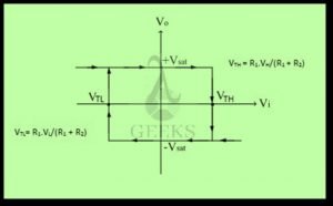
The above figure represents the output voltage versus the input voltage curve (which is also known as the voltage transfer characteristics), particularly showing the hysteresis effect. The transfer characteristic curve has two specific regions, the curve as the input voltage increases and the part of the curve in which the input voltage decreases. The voltage V+ does not have a constant value, but instead, it is a function of the output voltage V0.

Voltage transfer characteristics

In the voltage transfer characteristics, V= VH, or in high state. Then,

image007 10

Higher Cross-over voltage VTH

If signal is less than that of V+, the output stays at its high state. The cross-over voltage VTH occurs when V= V+ and expressed as follows:

image009 6

When Vi > VTH, the voltage at the inverting terminal is more than at the non-inverting terminal. Voltage V+ then turn out to be

image011 5

Lower Cross-over voltage VTL

Since V< VH the input voltage Vi is still more than V+, and the output rests in its low state as Vi carry on to increase; If Vi decreases, as long as the input voltage Vi is larger than V+, the output remains at saturation state. The cross-over voltage here and now occurs when V= V+ and this VTL expressed as

image013 10

As Vi continues to decrease, it remains less than V+; therefore, V0 remains in its high state. We can observe this transfer characteristic in the above figure. A hysteresis effect is shown in the net transfer characteristic diagram.

What is Schmitt trigger oscillator ?

Astable multivibrator or Schmitt trigger oscillator

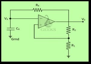
Astable multivibrator accomplished by fixing an RC network to the Schmitt trigger circuit in –ve feedback. As we will advance through the section, we will see that the circuit has no stable states and therefore, it also known as the astable multivibrator circuit.

Schmitt Trigger Oscillator
Astable Multivibrator circuit or Schmitt trigger Oscillator

As noticed in the figure, an RC network is set in the negative feedback path, and the inverting input terminal is connected to the ground through the capacitor while the non-inverting terminal is connected to the junction between the resistors R1 and R2 as shown in the figure.

At first, R1 and R2 is to be equal to R, and assume the output switches symmetrically about zero volts, with the high saturated output represented by V= VP and low saturated output indicated by V= -VP. If Vis low, or V= -VP, then V+ = -(1/2)VP.

When Vx drops just slightly below V+, the output switches to high so that V= +VP and V= +(1/2)VP. The equation for the voltage across the capacitor in an RC network can be expressed as:

image016

Where τx is the time constant which can be defined asτx= RxCx. The voltage Vx increases towards a final voltage VP in an exponential manner with respect to time. However, when Vx turn out to be slightly greater than V= +(1/2)VP, the output shifts to its low state of V0 = -VP and Vx = -(1/2)VP. The RxCx network gets triggered by a negative sharp transition of the voltages, and hence, the capacitor Cx start discharging, and the voltage Vx decreasing towards value of –VP. We can therefore express Vas

image022

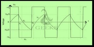
Where t1 refers to the time instant when the output of the circuit switches to its low state. The capacitor discharge exponentially V+ = -(1/2)VP, the output again shifts to high. The process repeats itself continuously over time, which means a square-wave output signal is produced by the oscillations of this positive feedback circuit. The figure below shows the output voltage V0 and the capacitor voltage Vx with respect to time.

Schmitt Trigger Oscillator Output voltage
The Schmitt Trigger Oscillator: Plot of Output voltage and Capacitor Voltage with respect to time

Time t1 can be found by substituting t=t1 and Vx = VP/2 in the general equation for the voltage across the capacitor.

image001 7

From the above equation when we solve for t1, we get

image003 7

For time t2 (as observed in the above figure), we approach in a similar way, and, from a similar analysis using the above equation, it is evident that the difference between t2 and t1 is also 1.1RxCx. From this, we can infer that the time period of oscillation T can be defined as T = 2.2 RxCx

And the frequency thus can be expressed as  

 image005 9

Duty cycle of Oscillator

The percentage of time the output voltage (V0) of the multi-vibrator is in its high state is particularly termed as the duty cycle of the oscillator.

The oscillator’s duty cycle is           

image007 11

As observed in the figure, depicting output voltage and capacitor voltage versus time, the duty cycle is 50%.

For more Electronics related article click here
Op-Amp As Integrator & Differentiator : Beginner’s Guide!

differentiator

Contents

  • What is Integrator?
  • Working principle of Integrator
  • Op-amp integrator circuit
  • Output of an integrator
  • Derivation of Op-amp as integrator
  • Practical op-amp integrator
  • Applications of integrator
  • What is Differentiator ?
  • Op-amp as Differentiator
  • Working Principle of Differentiator
  • Output waveform of a differentiator
  • Applications of Differentiator

What is Integrator?

Definition of Integrator

If the feedback path is made through a capacitor instead of a resistance , an RC Network has been established across the operational amplifiers’ negative feedback path. This kind of circuit configuration producing helps in implementing mathematical operation, specifically integration, and this operational amplifier circuit is known as an Operational amplifier Integrator circuit.

The output of the circuit is the integration of the applied input voltage with time.

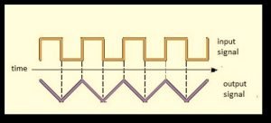
Integrator circuits are basically inverting operational amplifiers (they work in inverting op-amp configuration, with suitable capacitors and resistors), which generally produce a triangular wave output from a square wave input. Hence, they are also used for creating triangular pulses.

Op-amp as Integrator

Working principle of Integrator

Operational amplifiers can be used for mathematical applications such as Integration and Differentiation by implementing specific op-amp configurations.

When the feedback path is made through a capacitor instead of a resistance , an RC Network has been established across the operational amplifiers’ negative feedback path. This kind of circuit configuration producing helps in implementing mathematical operation, specifically integration, and this operational amplifier circuit is known as an Operational amplifier Integrator circuit. The output of the circuit is the integration of the applied input voltage with time.

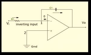
Op-amp integrator circuit

Integrator Circuit
Op-amp integrator circuit

Output of an integrator

Input Output of Integrator
input and output waveform of an integrator

Integrator circuits are basically inverting operational amplifiers (they work in inverting op-amp configuration, with suitable capacitors and resistors), which generally produce a triangular wave output from a square wave input. Hence, they are also used for creating triangular pulses.

The current in the feedback path is involved in the charging and discharging of the capacitor; therefore, the magnitude of the output signal is dependent on the amount of time a voltage is present (applied) at the input terminal of the circuit.

Derivation of Op-amp as integrator

As we know from the virtual ground concept, the voltage at point 1 is 0V. Hence, the capacitor is present between the terminals, one having zero potential and other at potential V0. When a constant voltage is applied at the input, it outcomes in a linearly increasing voltage (positive or negative as per the sign of the input signal) at the output whose rate of change is proportional to the value of the applied input voltage.

From the above circuitry it is observed, V1 = V2 = 0

The input current as:

aaa

Due to the op-amp characteristics (the input impedance of the op-amp is infinite) as the input current to the input of an op-amp is ideally zero. Therefore the current passing from the input resistor by applied input voltage Vi has flown along the feedback path into the capacitor C1.

Therefore the current from the output side can also be expressed as:

aaaa

Equating the above equations we get,

aaaaa

Therefore the op-amp output of this integrator circuit is:

b

As a consequence the circuit has a gain constant of -1/RC. The negative sign point toward an 180o phase shift.

Practical op-amp as aintegrator

If we apply a sine wave input signal to the integrator, the integrator allows low-frequency signals to pass while attenuates the high frequencies parts of the signal. Hence, it behaves like a low-pass filter rather than an integrator.

The practical integrator still has other limitations too. Unlike ideal op-amps, practical op-amps have a finite open-loop gain, finite input impedance, an input offset voltage, and an input bias current. This deviation from an ideal op-amp can affect working in several ways. For example, if Vin = 0, current passes through the capacitor due to the presence of both output offset voltage and input bias current. This causes the drifting of the output voltage over time till the op-amp saturates. If the input voltage current is zero in case of the ideal op-amp, then no drift should be present, but it is not true for the practical case.

To nullify the effect caused due to the input bias current, we have to modify the circuit such that Rom = R1||RF||RL

In this case, the error voltage will be 

bb

Therefore the same voltage drop appears at both the positive and negative terminals because of the input bias current.

For an ideal op-amp operating in the dc state, the capacitor performs as an open circuit, and hence, the gain of the circuit is infinite. To overcome this, a high resistance value resistor RF is connected in parallel with the capacitor in the feedback path. Because of this, the gain of the circuit is limited to a finite value (effectively small) and hence gets a small voltage error.

bbb
Practical Integrator
practical op-amp integrator
  • VIOS refers to the input offset voltage
  • IBI refers to the input bias current

What is Differentiator ?

Definition of Differentiator

If the input resistance in the inverting terminal is replaced by a capacitor, an RC Network has been established across the operational amplifiers’ negative feedback path. This kind of circuit configuration helps in implementing differentiation of the input voltage, and this operational amplifier circuit configuration is known as an Operational amplifier differentiator circuit.

An operational amplifier differentiator basically works as a high pass filter and, the amplitude of the output voltage produced by the differentiator is proportionate to the change of the applied input voltage.

Op-amp as a Differentiator

As we have studied earlier in the integrator circuit, op-amps can be used for implementing different mathematical applications. Here we will be studying the differential op-amp configuration in detail. The differentiator amplifier is also used for creating wave shapes and also in frequency modulators.

An operational amplifier differentiator basically works as a high pass filter and, the amplitude of the output voltage produced by the differentiator is proportionate to the change of the applied input voltage.

Working Principle of Differentiator

When the input resistance in the inverting terminal is replaced by a capacitor, an RC Network has been established across the operational amplifiers’ negative feedback path. This kind of circuit configuration helps in implementing differentiation of the input voltage, and this operational amplifier circuit configuration is known as an Operational amplifier differentiator circuit.

In a differentiating op-amp circuit, the output of the circuit is the differentiation of the input voltage applied to the op-amp with respect to time. Therefore the op-amp differentiator works in an inverting amplifier configuration, which causes the output to be 180 degrees out of phase with the input. Differentiating op-amp configuration generally responds to triangular or rectangular input waveforms.

A Differentiator Circuit

differentiators
Op-amp differentiator circuit

As shown in the figure, a connection of capacitor in series with the input voltage source has been made. The input capacitor C1 is initially uncharged and hence operate as an open-circuit. The non-inverting terminal of the amplifier is connected to the ground, whereas the inverting input terminal is through the negative feedback resistor Rf and connected to output terminal.

Due to the ideal op-amp characteristics (the input impedance of the op-amp is infinite) as the input current, I to the input of an op-amp is ideally zero. Therefore the current flowing through the capacitor (in this configuration, the input resistance is replaced by a capacitor) due to the applied input voltage Vin flows along the feedback path through the feedback resistor Rf.

As observed from the figure, point X is virtually grounded (according to the virtual ground concept) because the non-inverting input terminal is grounded (point Y is at ground potential i.e., 0V).

Consequently, Vx = Vy = 0

With respect to the input side capacitor, the current carrying through the capacitor can be written as:

cc

With respect to the output side feedback resistor, the current flowing through it can be represented as:

ccc

From the above equations when we equate the currents in both the results we get,

cccc
ccccc

The differentiating amplifier circuit requires a very small time constant for its application (differentiation), and hence it is one of its main advantages.

The product value C1Rf is known as differentiator’s time constant, and output of the differentiator is C1Rf times the differentiation of Vin signal. The -ve sign in the equation refers that the output is 180o difference in phase with reference to the input.

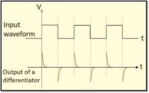
When we apply a constant voltage with one step change at t=0 like a step signal in the input terminal of the differentiator, the output should be ideally zero as the differentiation of constant is zero. But in practice, the output is not exactly zero because the constant input wave takes some amount of time to step from 0 volts to some Vmax volts. Therefore the output waveform appears to have a spike at time t=0.

Output Spike
Output waveform Containing spike

Therefore for a square wave input, we get something like shown in the below figure,

Output waveform
Output waveform of a differentiator for a square wave input

For more Electronics related article and their detail explanation  click here

.

7 Facts On Log & Antilog Amplifier:What,Working,Circuit,Use

log amplifier Symbol 300x154 1

The operational amplifier circuit configurations which can perform mathematical operations such as log and antilog (exponential), including an amplification of the input signal provided to the circuit, are known as Logarithmic amplifier and Antilogarithmic amplifier respectively. In this section, we are going to learn about the Logarithmic amplifier and Antilog in detail.

Contents:

  • Introduction
  • Logarithmic (Log) Amplifier
  • Log amplifier configuration
  • Diode based Log amplifier configuration
  • Transistor based Log amplifier configuration
  • Output and Working Principle of Log Amplifier
  • Applications of the log amplifier
  • What is Antilog?
  • Antilog Amplifier
  • Log amplifier configuration
  • Diode based antilog amplifier configuration
  • Transistor based antilog amplifier configuration
  • Output and Working Principle of Log Amplifier
  • Applications of the antilog amplifier

Logarithm (Log) Amplifier

An operational amplifier in which the output voltage of the amplifier (V0) is directly proportional to the natural logarithm of the input voltage (Vi) is known as a logarithmic amplifier. Basically, the natural logarithm of the input voltage is multiplied by a constant value and produced as output.

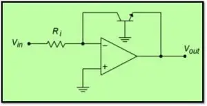
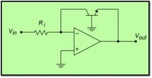
Log Amplifier Circuit

Log Amplifier Using Transistor

Log amplifier
Log amplifier using Transistor

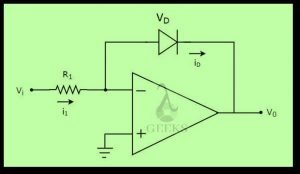
Log Amplifier using Diode

Log amplifier
Log amplifier using Diode

Output and Working Principle of Log Amplifier

This can be expressed as follows:

image002 2

Where K is the constant term, and Vref refers to a normalization constant, which we get to know in this section.

Generally, logarithm amplifiers may require more than one op-amp, in which case they are known as compensated logarithm amplifiers. They even require high performing op-amps for their proper functioning, such as LM1458, LM771, and LM714, are being some of the widely used logarithm amplifier.

The diode is connected in forward biasing. So, the diode current can be represented as:

image003 6

Where Is is the saturation current, VD is the voltage drop for the diode. The  VT is the thermal voltage. The diode current can be rewritten with high biasing condition,

image005 8

The i1 expressed by,

image007 9

Since the voltage at inverting terminal of the op-amp is at virtual ground, hence, the output voltage is given by V= -VD

Noting that i= iD, we can write

image010 3

But, as noted earlier, VD = -V0 and so,

image013 8

Taking natural logarithm on both sides of this equation, we found

image015 7

Or,  

image018 3                      

The equation of the output voltage (V0) of the logarithm amplifier contains a negative sign, which indicates that there is a phase difference of 180 o. Or, 

 image019 4                                                                       

A more advanced one utilize bipolar transistors to remove Is in the logarithmic term. In this type of logarithm amplifier configuration, the output voltage is given as:

image021 3

Applications of the logarithmic amplifier

Log amplifier is used for mathematical applications and also in different devices as per their need. Some of the applications of the log amplifier are as follows:

  • Log amplifiers are used for mathematical applications, mainly in multiplication. It is also used in the division and other exponential operations too. As it can perform multiplication operation, hence it is used in analog computers, in synthesizing audio effects, measuring instruments that require multiplication operation such as in calculating power (multiplication of current and voltage).
  • As we know that when we need to calculate the decibel equivalent of a given quantity, we require the use of a logarithmic operator, and hence, log amplifiers are used to calculate decibel (dB) value of a quantity.
  • Monolithic logarithmic amplifiers are used in certain situations, like in Radio Frequency domain, for efficient spacing (reducing components and space needed by them), and also to improve bandwidth and noise rejection.
  • It is also used in different ranges of applications such as rot mean square converter, an analog-to-digital converter, etc.

What is Antilog?

Antilog Amplifier

An Op-amp in which the output voltage of the amplifier (V0) is directly proportionate to the anti-log of the input voltage (Vi) is known as an anti-logarithmic amplifier or anti-log amplifier. Here, we are going to discuss the operational amplifier configuration that forms the anti-logarithmic amplifier in detail.

Antilog Amplifier Circuit

Antilog Amplifier Using Transistor

Antilog
Antilog Amplifier using Transistor

Antilog Amplifier using Diode

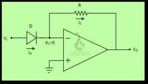
In the antilog amplifier, the input signal is at the inverting pin of the operational amplifier, which passes through a diode.

Antilog
Antilog Amplifier using Diode

Output and Working Principle of Antilog Amplifier

As observed in the circuit shown above, the negative feedback is achieved by connecting the output to the inverting input terminal. According to the concept of the virtual ground between the input terminals of an amplifier, the voltage V1 at the inverting terminal will be zero. Because of ideally infinite input impedance, the current flowing through the diode due to the applied input voltage in the inverting terminal will not enter the op-amp; instead, it will flow along the feedback path through the resistor R as shown in the figure.

The compliment or inverse function of the logarithmic amplifier is ‘exponential’,  anti-logarithmic or simply known as ‘antilog’. Consider the circuit given in the figure. The diode current is

image005 8

Where, VD is the diode voltage. According to the concept of virtual ground, V1=0 as the non-inverting terminal is grounded as shown in the figure. Therefore the voltage across the diode can be expressed as V= V– V1 or VD = Vi Hence, the current through the diode is

image025 2

Due to the ideal characteristics of an op-amp (infinite input impedance), the current flowing through the diode ( iD) flows along the feedback path through the resistor R, as we can observe in the figure.

Therefore i= i2

And, V0 = -i2R = -iDR

Replacing iD in the above equation we get 

image027 3

The parameters n, VT and Iare constants (they are only depend on the diode characteristics which are always constant for a particular diode). Therefore if the value of the feedback resistor R is fixed, then the output voltage V0 is directly proportional to the natural anti-logarithm (exponential) of the applied input voltage Vi. The above equation then can be simply represented as

 image031 3

Where K = – ISR and a = image033 1

Therefore we can notice that the anti-logarithmic op-amp produces its output signal as the exponential value of the input voltage signal applied.

The gain of the anti-log amplifier is given by the value of K that is equal to -ISR.

The –ve sign point out that there is a phase difference of 180degrees between the applied input s and the output of the anti-log amplifier.

For more Electronics related article click here
Inverting Operational Amplifier Trans Impedance Amp: A Comprehensive Guide

inverting operational amplifier trans impedance amp

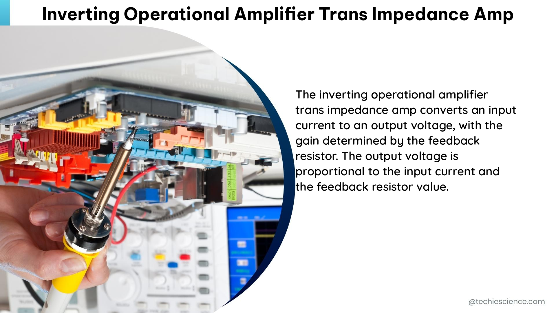
The inverting operational amplifier trans impedance amplifier (TIA) is a versatile circuit that converts a current input signal into a voltage output signal. This type of amplifier is commonly used with current-based sensors, such as photodiodes, due to its unique characteristics and performance advantages. In this comprehensive guide, we will delve into the technical details, design considerations, and practical applications of the inverting operational amplifier trans impedance amp.

Understanding the Inverting Operational Amplifier Trans Impedance Amp

The inverting operational amplifier trans impedance amplifier is a specialized circuit that leverages the properties of an operational amplifier (op-amp) to perform current-to-voltage conversion. The key feature of this circuit is its ability to maintain a high input impedance, which is crucial for accurately measuring and amplifying current-based signals.

Input Impedance Characteristics

One of the most interesting aspects of the inverting operational amplifier trans impedance amp is its input impedance behavior. Algebraically, the input impedance of this circuit is found to be proportional to the frequency and resembles the impedance of an inductor. The equivalent inductance can be calculated using the formula:

L_eq = R_f / (2 * π * f)

Where:
L_eq is the equivalent inductance
R_f is the feedback resistor
f is the frequency

This means that for low frequencies, the input impedance is high, while for high frequencies, the input impedance is low. This behavior can be attributed to the op-amp’s gain-bandwidth product, which determines the frequency range over which the amplifier maintains its desired characteristics.

Gain-Bandwidth Product

The gain-bandwidth product (GBW) of the op-amp used in the inverting operational amplifier trans impedance amp is a crucial parameter that affects the circuit’s performance. The gain at a given frequency is equal to the GBW divided by the frequency. This relationship is expressed as:

Gain = GBW / f

The GBW determines the frequency range over which the amplifier can maintain a stable and predictable gain. For frequencies much lower than the op-amp’s GBW, the input impedance is high, while for frequencies much higher than the GBW, the input impedance is low.

Input and Output Impedance Characteristics

The inverting operational amplifier trans impedance amp exhibits distinct input and output impedance characteristics:

  1. Input Impedance:
  2. At low frequencies (much lower than the op-amp’s GBW), the input impedance is high and proportional to the frequency, resembling the impedance of an inductor.
  3. At high frequencies (much higher than the op-amp’s GBW), the input impedance is low and looks like the impedance of a resistor with a value equal to the feedback resistor.

  4. Output Impedance:

  5. The output impedance of the inverting operational amplifier trans impedance amp is low, similar to other op-amp-based circuits.

These impedance characteristics make the TIA a superior choice for current-to-voltage conversion compared to using a simple resistor. The high input impedance at low frequencies allows for accurate measurement of current-based signals, while the low output impedance ensures efficient signal transfer to subsequent stages.

Design Considerations for Inverting Operational Amplifier Trans Impedance Amp

inverting operational amplifier trans impedance amp

When designing an inverting operational amplifier trans impedance amp, there are several key factors to consider to ensure optimal performance and meet the specific requirements of the application.
Feedback Resistor Selection

The feedback resistor, R_f, plays a crucial role in determining the overall gain and input impedance characteristics of the TIA. The value of R_f should be chosen carefully based on the following factors:

  1. Desired Transimpedance Gain: The transimpedance gain of the TIA is equal to the value of the feedback resistor, R_f. Higher values of R_f will result in higher transimpedance gain, but may also introduce stability issues and increase the equivalent inductance of the input impedance.

  2. Input Current Range: The maximum input current that the TIA can handle is limited by the maximum output voltage of the op-amp and the value of R_f. The maximum input current should be kept within the op-amp’s output voltage range to avoid saturation or clipping.

  3. Equivalent Inductance: As mentioned earlier, the equivalent inductance of the input impedance is inversely proportional to the frequency and directly proportional to the value of R_f. For slow op-amps and large transimpedances, the equivalent inductance can become quite significant, which may affect the circuit’s stability and frequency response.

Op-Amp Selection

The choice of the operational amplifier used in the TIA is critical, as it directly impacts the circuit’s performance and characteristics. Key parameters to consider when selecting an op-amp include:

  1. Gain-Bandwidth Product (GBW): The GBW of the op-amp determines the frequency range over which the amplifier maintains its desired characteristics. A higher GBW is generally preferred to extend the frequency range of the TIA.

  2. Input Offset Voltage: The input offset voltage of the op-amp can introduce errors in the current-to-voltage conversion, especially for low-level input currents. Op-amps with low input offset voltage are preferred for high-precision TIA designs.

  3. Input Bias Current: The input bias current of the op-amp can also contribute to errors in the current-to-voltage conversion. Op-amps with low input bias current are desirable for TIA applications.

  4. Slew Rate: The slew rate of the op-amp determines the maximum rate of change in the output voltage, which can be important for high-speed or high-frequency TIA applications.

  5. Noise Performance: The noise characteristics of the op-amp, such as input-referred voltage noise and current noise, can impact the signal-to-noise ratio of the TIA, especially for low-level input currents.

Stability Considerations

The inverting operational amplifier trans impedance amp can be susceptible to stability issues, particularly at high frequencies or with large values of R_f. To ensure stable operation, the following design considerations should be addressed:

  1. Compensation Capacitor: Adding a compensation capacitor, C_c, in parallel with the feedback resistor, R_f, can help stabilize the TIA by introducing a dominant pole and improving the phase margin.

  2. Bandwidth Limiting: Limiting the bandwidth of the TIA, either through the use of a low-pass filter or by selecting an op-amp with a lower GBW, can help improve the stability of the circuit.

  3. Feedback Resistor Value: As mentioned earlier, the value of R_f can significantly impact the equivalent inductance of the input impedance, which can lead to stability issues. Careful selection of R_f is crucial for maintaining stable operation.

  4. Parasitic Capacitances: Parasitic capacitances, such as those introduced by the op-amp, the feedback resistor, and the input wiring, can also affect the stability of the TIA. Minimizing these parasitic capacitances through proper layout and shielding techniques can help improve the circuit’s stability.

Applications of Inverting Operational Amplifier Trans Impedance Amp

The inverting operational amplifier trans impedance amp finds numerous applications in various fields, particularly in the realm of current-based sensor interfacing and signal conditioning.

Photodiode Amplifier

One of the most common applications of the TIA is as a photodiode amplifier. Photodiodes are current-based sensors that generate a current proportional to the incident light intensity. The TIA is an ideal choice for converting the photodiode’s current output into a voltage signal that can be further processed or measured.

Current Sensing

The TIA can also be used for general current sensing applications, where the input current is converted into a proportional voltage signal. This is useful in power management, motor control, and other systems where accurate current monitoring is required.

Electrochemical Sensor Interfaces

In the field of electrochemical sensing, the TIA is often employed to interface with current-based sensors, such as amperometric electrodes or ion-selective electrodes. The high input impedance of the TIA allows for accurate measurement of the small currents generated by these sensors.

Radiation Detection

In radiation detection systems, such as those used in medical imaging or nuclear instrumentation, the TIA is commonly used to amplify the current signals generated by radiation detectors, such as photodiodes or avalanche photodiodes (APDs).

Impedance Measurement

The unique input impedance characteristics of the TIA can be leveraged for impedance measurement applications. By monitoring the voltage output of the TIA, the input impedance of the circuit under test can be determined, which can be useful in various electrical and electronic characterization tasks.

Conclusion

The inverting operational amplifier trans impedance amplifier is a versatile and powerful circuit that plays a crucial role in a wide range of applications, particularly in the field of current-based sensor interfacing and signal conditioning. By understanding the technical details, design considerations, and practical applications of the TIA, electronics engineers and researchers can leverage this circuit to achieve accurate, stable, and efficient current-to-voltage conversion in their projects.

References:

  1. Operational Amplifier Circuits: Analysis and Design
  2. Analog Devices: Transimpedance Amplifier Design Guide
  3. Texas Instruments: Transimpedance Amplifier Basics
  4. Maxim Integrated: Transimpedance Amplifier Design Considerations
  5. Analog Devices: Op-Amp Stability Design and Compensation

Overview of Differential Amplifier Bridge Amplifier

overview differential amplifier bridge amplifier

A differential amplifier bridge amplifier is a specialized electronic circuit that combines the functionality of a differential amplifier and a bridge amplifier. It is widely used in applications that require high precision, noise immunity, and the ability to amplify small voltage differences, such as strain gauge measurements and data acquisition systems.

Technical Specifications

Gain

  • The gain of a differential amplifier bridge amplifier is typically high, ranging from 50 to 100. This high gain allows for the effective amplification of small voltage differences between the input signals.

Input Voltage Range

  • The input voltage range of a differential amplifier bridge amplifier depends on the specific operational amplifier (op-amp) used in the circuit. For example, the LM358 op-amp can handle input voltages up to 32V, while the TLV2772A op-amp can handle input voltages up to 36V.

Common-Mode Rejection Ratio (CMRR)

  • The CMRR of a differential amplifier bridge amplifier is typically high, often exceeding 80 dB. This high CMRR ensures that the amplifier effectively rejects common-mode noise and only amplifies the desired differential signal.

Noise Immunity

  • Differential amplifier bridge amplifiers are highly resistant to external noise sources due to their differential signaling architecture. This makes them suitable for use in noisy environments, where they can maintain high accuracy and reliability.

Output Voltage Swing

  • The output voltage swing of a differential amplifier bridge amplifier can be quite high, often up to 90% of the supply voltage. This large output voltage range allows the amplifier to be used in a variety of applications.

Physics and Theoretical Explanation

overview differential amplifier bridge amplifier

The operation of a differential amplifier bridge amplifier is based on the principles of differential signaling and amplification. The amplifier takes two input signals, V1 and V2, and amplifies their difference, Vdm = V1 - V2. This is achieved through a combination of resistors and op-amps that create a differential gain stage.

The output voltage of the amplifier can be expressed as:

Vout = KVdm + Vref

where K is the gain of the amplifier and Vref is the reference voltage.

Examples and Numerical Problems

Strain Gauge Measurement

Consider a strain gauge connected to a Wheatstone bridge, which is then connected to a differential amplifier bridge amplifier. If the strain gauge resistance changes from 350 Ohms to 351 Ohms, the output voltage of the bridge changes from -5.365 mV to -5.365 mV + 134 mV = 128.635 mV.

Differential Gain Calculation

Given a differential amplifier bridge amplifier with resistors R1 = R2 = 1 kΩ and R3 = R4 = 50 kΩ, calculate the differential gain K.

K = R3/R1 = 50 kΩ/1 kΩ = 50

Figures and Data Points

Circuit Diagram

A typical differential amplifier bridge amplifier circuit consists of a Wheatstone bridge connected to a differential amplifier stage, which is then followed by additional gain stages.

Output Voltage vs. Input Voltage

The output voltage of the amplifier increases linearly with the differential input voltage, with a slope determined by the gain of the amplifier.

Measurements and Applications

Strain Gauge Measurements

Differential amplifier bridge amplifiers are commonly used in strain gauge measurements to amplify the small voltage changes produced by the strain gauge. This allows for accurate monitoring and analysis of mechanical deformation in various structures and materials.

Data Acquisition Systems

These amplifiers are also used in data acquisition systems to amplify and condition signals from various sensors, ensuring high accuracy and noise immunity. This is particularly important in applications where the input signals are weak or susceptible to interference, such as in industrial automation, biomedical instrumentation, and environmental monitoring.

References

  1. Electronics Tutorials. (n.d.). Differential Amplifier – The Voltage Subtractor. Retrieved from https://www.electronics-tutorials.ws/opamp/opamp_5.html
  2. Texas Instruments. (2002). Fully-Differential Amplifiers (Rev. E). Retrieved from https://www.ti.com/lit/an/sloa054e/sloa054e.pdf
  3. Embedded Related. (2014). How to Analyze a Differential Amplifier. Retrieved from https://www.embeddedrelated.com/showarticle/557.php
  4. Curious Scientist. (2023). Strain gauge, Wheatstone bridge, differential amplifier – Educational device. Retrieved from https://curiousscientist.tech/blog/strain-gauge-wheatstone-bridge-differential-amplifier-educational-device
  5. NI Community. (2014). op amp differential amplifier measurements. Retrieved from https://forums.ni.com/t5/LabVIEW/op-amp-differential-amplifier-measurements/td-p/2861666

Faraday’s Law of Induction, Lenz’s Law, and Magnetic Flux: A Comprehensive Guide

faradays law of induction lenzs law

Faraday’s Law of Induction and Lenz’s Law are fundamental principles in electromagnetism that describe the relationship between changing magnetic fields and the induced electromotive forces (EMFs) they create. These laws are essential for understanding the behavior of various electromagnetic devices, from transformers and generators to induction motors and wireless charging systems. In this comprehensive guide, we will delve into the mathematical formulations, key concepts, practical applications, and numerical examples related to these important laws.

Faraday’s Law of Induction

Faraday’s Law of Induction states that the induced EMF in a circuit is proportional to the rate of change of the magnetic flux through the circuit. The mathematical expression for Faraday’s Law is:

[
\text{emf} = -N \frac{\Delta \Phi}{\Delta t}
]

Where:
emf: Electromotive force (volts, V)
N: Number of turns in the coil
ΔΦ: Change in magnetic flux (weber, Wb)
Δt: Time over which the flux changes (seconds, s)

The negative sign in the equation indicates that the induced EMF opposes the change in magnetic flux, as described by Lenz’s Law.

Magnetic Flux

Magnetic flux, denoted as Φ, is a measure of the total magnetic field passing through a given surface or area. The formula for magnetic flux is:

[
\Phi = B \cdot A \cdot \cos \theta
]

Where:
Φ: Magnetic flux (weber, Wb)
B: Magnetic field strength (tesla, T)
A: Area of the coil (square meters, m²)
θ: Angle between the magnetic field and the coil normal (degrees)

The magnetic flux is directly proportional to the magnetic field strength, the area of the coil, and the cosine of the angle between the magnetic field and the coil normal.

Lenz’s Law

faradays law of induction lenzs law flux

Lenz’s Law states that the direction of the induced current in a circuit is such that it opposes the change in the magnetic flux that caused it. In other words, the induced current will create a magnetic field that opposes the original change in the magnetic field.

To determine the direction of the induced current, you can use the right-hand rule:
1. Point your thumb in the direction of the magnetic field.
2. Curl your fingers around the coil or circuit.
3. The direction your fingers curl is the direction of the induced current.

This rule helps you visualize the direction of the induced current and ensures that it opposes the change in the magnetic flux, as described by Lenz’s Law.

Examples and Applications

Induction Cooker

  • Magnetic Field Strength: Typically around 100 mT (millitesla)
  • Frequency: 27 kHz (kilohertz)
  • Induced EMF: High values due to the high rate of change of the magnetic field

Induction cookers use the principles of electromagnetic induction to heat cookware. The rapidly changing magnetic field induces a high EMF in the metal cookware, which in turn generates heat through eddy currents.

Transformer

  • Mutual Inductance: The ability of two coils to induce EMFs in each other
  • Efficiency: Transformers can achieve high efficiency (up to 99%) due to the principles of electromagnetic induction

Transformers rely on the mutual inductance between two coils to step up or step down the voltage in an electrical system. The changing magnetic field in the primary coil induces a corresponding EMF in the secondary coil, allowing for efficient power transformation.

Electric Generator

  • EMF: Varies sinusoidally with time
  • Angular Velocity: The coil is rotated at a constant angular velocity to produce the EMF

Electric generators convert mechanical energy into electrical energy by using the principles of electromagnetic induction. As a coil is rotated in a magnetic field, the changing magnetic flux induces an EMF that varies sinusoidally with time.

Numerical Problems

Example 1

  • Change in Flux: 2 Wb to 0.2 Wb in 0.5 seconds
  • Induced EMF: Calculate the induced EMF using Faraday’s Law

Solution:
[
\Delta \Phi = 0.2 – 2 = -1.8 \text{ Wb}
]
[
\text{emf} = -N \frac{\Delta \Phi}{\Delta t} = -N \frac{-1.8}{0.5} = 3.6 N \text{ V}
]

Example 2

  • Coil Area: 0.1 m²
  • Magnetic Field Strength: 0.5 T
  • Angle: 30°
  • Number of Turns: 100
  • Time: 0.2 seconds
  • Change in Flux: Calculate the change in flux and the induced EMF

Solution:
[
\Phi = B \cdot A \cdot \cos \theta = 0.5 \cdot 0.1 \cdot \cos 30° = 0.043 \text{ Wb}
]
[
\Delta \Phi = 0.043 \text{ Wb}
]
[
\text{emf} = -N \frac{\Delta \Phi}{\Delta t} = -100 \frac{0.043}{0.2} = -21.5 \text{ V}
]

References

  1. Lumen Learning. (n.d.). Faraday’s Law of Induction: Lenz’s Law. Retrieved from https://courses.lumenlearning.com/suny-physics/chapter/23-2-faradays-law-of-induction-lenzs-law/
  2. Boundless Physics. (n.d.). Magnetic Flux, Induction, and Faraday’s Law. Retrieved from https://www.collegesidekick.com/study-guides/boundless-physics/magnetic-flux-induction-and-faradays-law
  3. ScienceDirect. (n.d.). Faraday’s Law. Retrieved from https://www.sciencedirect.com/topics/physics-and-astronomy/faradays-law
  4. GeeksforGeeks. (2022). Faraday’s Law of Electromagnetic Induction: Experiment & Formula. Retrieved from https://www.geeksforgeeks.org/faradays-law/
  5. Science in School. (2021). Faraday’s law of induction: from classroom to kitchen. Retrieved from https://www.scienceinschool.org/article/2021/faradays-law-induction-classroom-kitchen/

Transformer Equations Working Energy Loss: A Comprehensive Guide

transformer equations working energy loss

Transformer equations play a crucial role in understanding and quantifying the energy losses associated with transformer operations. This comprehensive guide delves into the technical details, data points, and research insights that shed light on the complex dynamics of transformer energy losses, equipping physics students with a robust understanding of this essential topic.

Transformer Losses Due to Harmonics

Harmonics, which are distortions in the sinusoidal waveform of the electrical supply, can significantly contribute to energy losses in transformers. Let’s explore the quantifiable data points that illustrate the impact of harmonics on transformer performance:

Transformer Losses

  1. Total Losses in Transformer Due to Harmonics: 3.7 kW
  2. Cable Losses Due to Harmonics: 0.74 kW
  3. Total Savings After Installation of Filter: 4.4 kW

These figures demonstrate the substantial energy losses that can be attributed to harmonics in the electrical system, highlighting the importance of implementing effective mitigation strategies.

Power Factor Improvement

  1. Power Factor Before Installation of Advanced Universal Passive Harmonic Filter: Not specified
  2. Power Factor After Installation of Advanced Universal Passive Harmonic Filter: 0.99

The significant improvement in power factor, from an unspecified value to 0.99, illustrates the positive impact of the harmonic filter on the overall power quality and efficiency of the transformer system.

KVA Reduction

  1. KVA Before Installation of Filter: 88.6 KVA
  2. KVA After Installation of Filter: 68.5 KVA
  3. Total KVA Savings: 20 KVA

The reduction in KVA, from 88.6 to 68.5, showcases the substantial capacity savings achieved through the installation of the harmonic filter, further enhancing the overall efficiency and performance of the transformer.

Return on Investment (ROI)

  1. Filter Cost: ₹2,10,000
  2. Total Savings Per Year: ₹3,62,112
  3. ROI: 7 months

The impressive return on investment, with a payback period of just 7 months, underscores the financial benefits of implementing effective harmonic mitigation strategies in transformer systems.

Loss Reduction Strategies

transformer equations working energy loss

Alongside the quantifiable data on the impact of harmonics, various loss reduction strategies have been explored in the research, offering valuable insights for physics students:

Line Loss Interval

  1. Line Loss Interval Estimation: A model can estimate the reasonable line loss interval based on transformer operation data.

This approach allows for a more accurate assessment of line losses, enabling better optimization and management of the transformer system.

Loss Modelling

  1. Accurate Loss Modelling: Static piecewise linear loss approximation based on line loading classification can achieve accurate loss modelling.

Precise loss modelling is crucial for understanding the energy dynamics within the transformer and developing effective strategies to minimize losses.

Line Loss Calculation

  1. Line Loss Calculation Method: A method based on big data and load curve can be used for line loss calculation.

The utilization of big data and load curve analysis provides a comprehensive approach to estimating and managing line losses, contributing to the overall efficiency of the transformer system.

Energy Conservation Standards

Regulatory bodies, such as the U.S. Department of Energy (DOE), have established guidelines and standards to promote energy efficiency in transformer systems. These standards offer valuable insights for physics students:

Energy Efficiency

  1. DOE Guidance: The U.S. Department of Energy (DOE) advises on analytical methods, data sources, and key assumptions for energy conservation standards in distribution transformers.

Understanding these energy conservation standards and the underlying analytical approaches can help physics students develop a deeper understanding of the regulatory landscape and its impact on transformer design and operation.

Research on Transformer Operation

The research landscape on transformer operation has yielded valuable insights that can enhance the understanding of physics students:

Fuzzy Comprehensive Evaluation

  1. Transformer Working State Evaluation: A multi-level evaluation method based on key performance indicators can be used to evaluate the working state of transformers.

This comprehensive evaluation approach provides a holistic assessment of transformer performance, enabling better monitoring and optimization of the system.

Transformer Losses and Temperature Rise

  1. Correlations in Transformer Operation: The heating temperature rise has correlations to the loading current, power losses, efficiency, and surface area.

Exploring these correlations between transformer parameters can help physics students develop a more nuanced understanding of the complex relationships that govern transformer energy losses and efficiency.

By delving into the technical details, data points, and research insights presented in this comprehensive guide, physics students can gain a deeper understanding of the intricate dynamics of transformer equations and their impact on energy losses. This knowledge will equip them with the necessary tools to tackle real-world challenges in the field of power systems and transformer design.

References

  1. https://www.linkedin.com/pulse/incredible-power-losses-caused-harmonics-measurable-waveforms
  2. https://www.sciencedirect.com/science/article/abs/pii/S0306261921014021
  3. https://www1.eere.energy.gov/buildings/appliance_standards/pdfs/dt_nopr_tsd_complete.pdf
  4. https://link.springer.com/chapter/10.1007/978-981-97-3940-0_6
  5. https://www.researchgate.net/publication/326317282_Investigation_of_transformer_losses_and_temperature_rise

Hall Effect Sensor Magnetic Sensors Applications: A Comprehensive Guide

hall effect sensor magnetic sensors applications

Hall effect sensors are versatile devices that have found widespread applications in various industries, from automotive to medical and industrial applications. These sensors leverage the Hall effect, a fundamental principle in physics, to detect and measure magnetic fields, enabling a wide range of functionalities. In this comprehensive guide, we will delve into the technical details, theoretical explanations, and practical applications of hall effect sensor magnetic sensors.

Automotive Applications

Seat and Safety Belt Position Sensing

Hall effect sensors are used in vehicles to detect the position of seats and safety belts, ensuring that the appropriate safety features are activated. These sensors monitor the position of the seat and safety belt, providing feedback to the vehicle’s control systems to optimize occupant protection.

Windshield Wiper Position Sensing

Hall effect sensors are employed to monitor the position of windshield wipers, enabling precise control and ensuring proper operation. By detecting the wiper’s position, the vehicle’s control systems can synchronize the wiper movement with other systems, such as the rain sensor, to enhance driving visibility and safety.

Brake and Gas Pedal Position Sensing

Hall effect sensors are utilized to detect the position and movement of brake and gas pedals in vehicles. This information is crucial for the vehicle’s safety and control systems, as it allows for the precise monitoring and regulation of the pedal inputs, enhancing overall driving performance and responsiveness.

Ignition System Position Sensing

Hall effect sensors play a vital role in the ignition system of vehicles, detecting the position of the ignition switch. This information is used to ensure proper engine operation, enabling the vehicle’s control systems to synchronize the ignition timing and other engine-related functions.

Industrial Applications

hall effect sensor magnetic sensors applications

Current Measurement

Hall effect sensors can be employed to measure current by detecting the magnetic field generated by the current flow. This capability is valuable for monitoring the performance and ensuring the safety of industrial equipment, as it allows for the continuous monitoring of current levels and the detection of any abnormalities.

Gear Tooth Sensing

Hall effect sensors are used to detect the presence or absence of gear teeth, enabling accurate gear position detection and control. This application is crucial in industrial machinery, where precise gear positioning is essential for efficient operation and performance.

Proximity Detection

Hall effect sensors are utilized in industrial settings for proximity detection, identifying the presence or absence of objects. This functionality is valuable in applications such as door sensors, object detection systems, and various automation processes.

Medical and Biomedical Applications

Magnetic Bead Detection

In biomedical applications, Hall effect sensors are employed to detect magnetic beads, which are commonly used in immunoassays and protein detection. These sensors can precisely identify the presence and location of the magnetic beads, enabling advanced diagnostic and research capabilities.

Magnetic Nanoparticle Detection

Hall effect sensors are also used to detect magnetic nanoparticles, which have numerous applications in biomedical research and diagnostics. These sensors can provide valuable insights into the behavior and distribution of magnetic nanoparticles, contributing to advancements in areas such as drug delivery, biosensing, and medical imaging.

Other Applications

Fluid Flow Sensing

Hall effect sensors can be used to detect changes in fluid flow by measuring the magnetic field generated by the fluid flow. This application is beneficial in various industries, including process control, automation, and environmental monitoring.

Pressure Sensing

Hall effect sensors can be employed to detect changes in pressure by measuring the magnetic field generated by the pressure changes. This capability is useful in applications such as industrial process control, automotive systems, and medical devices.

Building Automation

Hall effect sensors are utilized in building automation systems to detect the presence or absence of objects, such as in door sensors or object detection systems. This functionality contributes to the optimization of building operations, energy efficiency, and security.

Technical Specifications

Sensitivity

Hall effect sensors can detect magnetic fields as low as a few microtesla (μT), making them highly sensitive to even small changes in magnetic fields.

Resolution

Hall effect sensors can achieve a resolution as high as 1 microtesla (μT), enabling precise measurements of magnetic field variations.

Operating Frequency

Hall effect sensors can operate at frequencies up to 100 kilohertz (kHz), allowing for high-speed applications and real-time monitoring.

Power Consumption

Hall effect sensors typically consume low power, often in the range of milliwatts (mW), making them suitable for battery-powered or energy-efficient applications.

Theoretical Explanation

The Hall effect is a fundamental principle in physics that describes the generation of a voltage perpendicular to both the direction of current flow and the applied magnetic field. When a current-carrying conductor or semiconductor is placed in a magnetic field, the magnetic field exerts a force on the moving charge carriers, causing them to accumulate on one side of the material. This accumulation of charge carriers results in the generation of a voltage, known as the Hall voltage, which is proportional to the strength of the magnetic field and the current flowing through the material.

Physics Formulae

Hall Voltage

The Hall voltage (V_H) can be calculated using the following formula:

V_H = (G * t * N * r_n * q * I_bias * B) / (e * n)

Where:
– G is the geometric factor
– t is the thickness of the Hall device
– N is the impurity concentration
– r_n is the Hall factor
– q is the charge per unit charge
– I_bias is the bias current
– B is the applied magnetic field strength
– e is the elementary charge
– n is the carrier concentration

Magnetic Flux

The magnetic flux (Φ) can be calculated using the formula:

Φ = B * A

Where:
– B is the magnetic field strength
– A is the area of the sensing unit normal to the magnetic field

References

  1. Arrow Electronics. (2023). Hall Effect Sensor Applications. Retrieved from https://www.arrow.com/en/research-and-events/articles/hall-effect-sensor-applications
  2. Allegro MicroSystems. (n.d.). Hall Effect Sensor | Applications Guide. Retrieved from https://www.allegromicro.com/en/insights-and-innovations/technical-documents/hall-effect-sensor-ic-publications/hall-effect-ic-applications-guide
  3. Detection techniques of biological and chemical Hall sensors. (2021). PMC. Retrieved from https://www.ncbi.nlm.nih.gov/pmc/articles/PMC8695063/
  4. RS Components. (n.d.). Everything You Need To Know About Hall Effect Sensors. Retrieved from https://se.rs-online.com/web/generalDisplay.html?id=ideas-and-advice%2Fhall-effect-sensors-guide
  5. Makeability Lab. (n.d.). Hall Effect Sensors. Retrieved from https://makeabilitylab.github.io/physcomp/sensors/hall-effect.html

Eddy Currents and Electromagnetic Damping: A Comprehensive Guide

eddy currents electromagnetic damping application

Eddy currents and their applications in electromagnetic damping are crucial in various fields, from laboratory equipment to industrial processes. This comprehensive guide delves into the quantitative analysis of eddy current damping, its theoretical background, and a wide range of practical applications.

Quantitative Analysis of Eddy Current Damping

Damping Coefficients

Researchers have conducted laboratory experiments to measure the damping coefficients for different magnet and track combinations. The results provide valuable insights into the effectiveness of eddy current damping:

Combination Damping Coefficient (N s m⁻¹)
Cu1-A 0.039 ± 0.001
Cu3-A 0.081 ± 0.001
Cu1-M1 0.194 ± 0.001
Cu3-M1 0.378 ± 0.001

These measurements demonstrate the significant impact of the magnet and track materials on the damping coefficient, with the Cu3-M1 combination exhibiting the highest damping effect.

Kinetic Friction Coefficients

In addition to damping coefficients, researchers have also measured the kinetic friction coefficients for the same magnet and track combinations:

Combination Kinetic Friction Coefficient
Cu1-A 0.22 ± 0.02
Cu3-A 0.21 ± 0.01
Cu1-M1 0.20 ± 0.04
Cu3-M1 0.20 ± 0.01

These values provide a comprehensive understanding of the frictional forces involved in eddy current damping systems, which is crucial for designing and optimizing various applications.

Applications of Eddy Currents and Magnetic Damping

eddy currents electromagnetic damping application

Magnetic Damping in Laboratory Balances

Magnetic damping is widely used in laboratory balances to minimize oscillations and maximize sensitivity. The drag force created by eddy currents is proportional to the speed of the moving object, and it becomes zero at zero velocity, allowing for precise measurements.

Metal Separation in Recycling

Eddy currents are employed in recycling centers to separate metals from non-metals. The conductive metals are slowed down by the magnetic damping effect, while the non-metals continue to move, enabling efficient separation and recovery of valuable materials.

Metal Detectors

Portable metal detectors utilize the principle of eddy currents to detect the presence of metals. These devices consist of a coil that generates a magnetic field, which induces eddy currents in nearby conductive objects, allowing for their detection.

Braking Systems

Eddy currents are employed in braking systems for high-speed applications, such as trains and roller coasters. The induced eddy currents create a braking force that slows down the moving objects, providing an effective and reliable means of deceleration.

Theoretical Background

Eddy Current Generation

Eddy currents are generated when a conductor moves in a magnetic field or when a magnetic field moves relative to a conductor. This phenomenon is based on the principle of motional electromotive force (emf), where the relative motion between the conductor and the magnetic field induces a voltage, which in turn generates the eddy currents.

The magnitude of the induced eddy currents is proportional to the rate of change of the magnetic field and the electrical conductivity of the material. The direction of the eddy currents is such that they oppose the change in the magnetic field, as described by Lenz’s law.

Magnetic Damping

Magnetic damping occurs when the eddy currents induced in a moving conductor produce a drag force that opposes the motion. This drag force is proportional to the velocity of the conductor and the strength of the magnetic field. The damping force acts to dissipate the kinetic energy of the moving object, effectively slowing it down.

The mathematical expression for the magnetic damping force is given by:

F_d = -b * v

Where:
– F_d is the damping force
– b is the damping coefficient
– v is the velocity of the moving object

The damping coefficient, b, depends on the geometry of the system, the magnetic field strength, and the electrical conductivity of the material.

Conclusion

Eddy currents and electromagnetic damping have a wide range of applications in various fields, from laboratory equipment to industrial processes. The quantitative analysis of damping coefficients and kinetic friction coefficients provides valuable insights into the performance and optimization of these systems. Understanding the theoretical background of eddy current generation and magnetic damping is crucial for designing and implementing effective solutions in diverse applications.

References

  1. Molina-Bolivar, J. A., & Abella-Palacios, A. J. (2012). A laboratory activity on the eddy current brake. European Journal of Physics, 33(3), 697-706. doi: 10.1088/0143-0807/33/3/697
  2. Lumen Learning. (n.d.). Eddy Currents and Magnetic Damping. Retrieved from https://courses.lumenlearning.com/suny-physics/chapter/23-4-eddy-currents-and-magnetic-damping/
  3. Griffiths, D. J. (2013). Introduction to Electromagnetism (4th ed.). Pearson.
  4. Halliday, D., Resnick, R., & Walker, J. (2013). Fundamentals of Physics (10th ed.). Wiley.

Overview of Magnets: Electromagnets, Permanent, Hard, and Soft

overview magnets electromagnet permanent hard soft

Magnets are materials that produce a magnetic field, which can attract or repel other magnetic materials. Understanding the different types of magnets and their properties is crucial in various applications, from electric motors and generators to medical imaging and data storage. In this comprehensive guide, we will delve into the measurable and quantifiable data on electromagnets, permanent magnets, hard magnets, and soft magnets.

Permanent Magnets

Permanent magnets are materials that can maintain a magnetic field without the need for an external source of electricity. These magnets are characterized by several key properties:

Magnetic Field Strength

The magnetic field strength of a permanent magnet is a measure of the intensity of the magnetic field it produces. The strength of the magnetic field is typically measured in Tesla (T) or Gauss (G). Neodymium (NdFeB) magnets, for example, can have a magnetic field strength of up to 1.4 T, while samarium-cobalt (SmCo) magnets can reach around 1.1 T.

Coercivity

Coercivity, also known as the coercive force, is the measure of a permanent magnet’s resistance to demagnetization. It is the strength of the external magnetic field required to reduce the magnetization of the material to zero. Permanent magnets with high coercivity, such as NdFeB (around 1.9 T) and SmCo (around 4.4 T), are more resistant to demagnetization.

Remanence

Remanence, or residual magnetization, is the measure of the magnetic flux density that remains in a material after an external magnetic field is removed. Permanent magnets with high remanence, such as NdFeB (around 32.5 μB per formula unit) and SmCo (around 8 μB per formula unit), can maintain a strong magnetic field even without an external source.

Curie Temperature

The Curie temperature is the temperature above which a ferromagnetic material loses its ferromagnetic properties and becomes paramagnetic. For permanent magnets, the Curie temperature is an important consideration, as it determines the maximum operating temperature. NdFeB magnets have a Curie temperature of around 312°C, while SmCo magnets can withstand higher temperatures, up to around 800°C.

Electromagnets

overview magnets electromagnet permanent hard soft

Electromagnets are devices that produce a magnetic field when an electric current flows through a coil of wire. Unlike permanent magnets, the magnetic field of an electromagnet can be turned on and off, and its strength can be adjusted by controlling the electric current.

Magnetic Field Strength

The magnetic field strength of an electromagnet is directly proportional to the electric current flowing through the coil. The strength can be calculated using the formula:

B = μ₀ * N * I / L

Where:
– B is the magnetic field strength (in Tesla)
– μ₀ is the permeability of free space (4π × 10^-7 T⋅m/A)
– N is the number of turns in the coil
– I is the electric current (in Amperes)
– L is the length of the coil (in meters)

The magnetic field strength of an electromagnet can be varied by adjusting the electric current, making them useful in applications where a controllable magnetic field is required.

Coercivity and Remanence

Electromagnets do not have a fixed coercivity or remanence, as their magnetic properties are entirely dependent on the electric current flowing through the coil. When the current is turned off, the electromagnet loses its magnetization, and there is no residual magnetic field.

Curie Temperature

Electromagnets do not have a Curie temperature, as they are not made of ferromagnetic materials. The magnetic field is generated by the flow of electric current, rather than the alignment of magnetic domains within the material.

Hard Magnets

Hard magnets, also known as permanent magnets, are materials that can maintain a strong, persistent magnetic field. These magnets are characterized by their high coercivity and remanence, making them resistant to demagnetization.

Coercivity

The coercivity of hard magnets is a measure of their resistance to demagnetization. Materials with high coercivity, such as NdFeB (around 1.9 T) and SmCo (around 4.4 T), are considered “hard” magnets and are less susceptible to losing their magnetization.

Remanence

Hard magnets have a high remanence, meaning they can retain a significant amount of magnetization even after the external magnetic field is removed. For example, the remanence of NdFeB magnets is around 32.5 μB per formula unit, and for SmCo magnets, it is around 8 μB per formula unit.

Curie Temperature

The Curie temperature of hard magnets is an important consideration, as it determines the maximum operating temperature before the material loses its ferromagnetic properties. NdFeB magnets have a Curie temperature of around 312°C, while SmCo magnets can withstand higher temperatures, up to around 800°C.

Soft Magnets

Soft magnets are materials that can be easily magnetized and demagnetized. They are characterized by their low coercivity and remanence, making them suitable for applications where a variable magnetic field is required.

Coercivity

The coercivity of soft magnets is relatively low, typically around 0.080 T for iron and 0.40 T for ferrites. This low coercivity allows soft magnets to be easily magnetized and demagnetized.

Remanence

Soft magnets have a low remanence, meaning they retain a relatively small amount of magnetization after the external magnetic field is removed. For instance, the remanence of iron is around 1.2 T, and that of ferrites is around 0.5 T.

Curie Temperature

The Curie temperature of soft magnets is generally lower than that of hard magnets. For example, the Curie temperature of iron is around 770°C.

Magnetic Hysteresis

Magnetic hysteresis is the phenomenon where the magnetization of a material depends on its magnetic history. This behavior is characterized by the material’s hysteresis loop, which is defined by the remanence (M_r) and coercivity (H_c) of the material.

Hysteresis Loop

The hysteresis loop represents the relationship between the applied magnetic field (H) and the resulting magnetization (M) of a material. The shape of the loop is determined by the material’s magnetic properties, such as coercivity and remanence.

Energy Loss

The area enclosed by the hysteresis loop represents the energy lost during each magnetization cycle, known as hysteresis loss. This energy loss is an important consideration in the design of magnetic devices, as it can contribute to inefficiencies and heat generation.

Other Quantifiable Data

In addition to the properties discussed above, there are other quantifiable data points that are relevant to the understanding of magnets:

Magnetic Energy Product

The magnetic energy product is a measure of the energy stored in a magnetic field. It is calculated as the product of the magnetic field strength (B) and the magnetic field intensity (H). High-energy permanent magnets, such as NdFeB, can have a magnetic energy product of up to 450 kJ/m³.

Hall Coefficient

The Hall coefficient is a measure of the Hall effect, which is the generation of a voltage difference across a material when a magnetic field is applied. The Hall coefficient is typically measured in units of m³/C and is used in Hall effect sensors to measure magnetic fields.

By understanding the measurable and quantifiable data on electromagnets, permanent magnets, hard magnets, and soft magnets, you can gain a deeper insight into the properties and applications of these materials. This knowledge can be invaluable in fields such as electrical engineering, materials science, and physics.

References:

  1. Adams Magnetic Products. (n.d.). Permanent Magnets vs Electromagnets. Retrieved from https://www.adamsmagnetic.com/permanent-magnets-vs-electromagnets/
  2. Nature. (2021). A hard permanent magnet through molecular design. Retrieved from https://www.nature.com/articles/s42004-021-00509-y
  3. ScienceDirect. (n.d.). Magnetic Energy Product – an overview. Retrieved from https://www.sciencedirect.com/topics/chemistry/magnetic-energy-product
  4. ResearchGate. (n.d.). Advanced Permanent Magnetic Materials. Retrieved from https://www.researchgate.net/publication/270567539_Advanced_Permanent_Magnetic_Materials
  5. Wevolver. (2024). What is Magnetism? Examples of Magnetic Substances. Retrieved from https://www.wevolver.com/article/rigid-pcb