Filter Capacitor: 23 Important Facts You Should Know

437339684 f643935543 b

Content:

What is a Filter Capacitor?

The capacitor’s impedance can be defined as a function of frequency as the capacitor is a reactive element, it is suitable for using it as an analog electronics filter.

A filter capacitor is a passive filter that consists of the passive element. Capacitor effects of any signal are frequency-dependent. This capacitor characteristic is used to design filters that can filter out a specific frequency range of signals as required.

Filter Capacitor Image

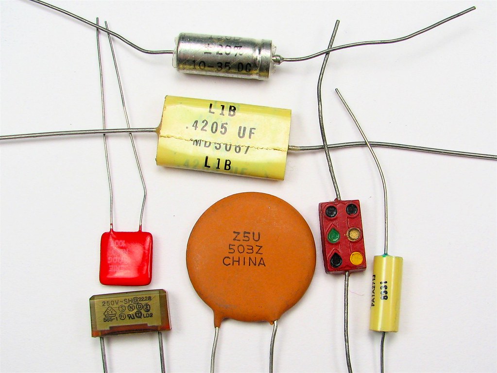
Capacitors
Image Credit: “Capacitors” by oskay is licensed under CC BY 2.0

Working of Filter Capacitor

The capacitor is a reactive circuit element; its impedance and resistance will vary with the frequency signal passing through it.

The working of the filter-capacitor is based on the fundamental principle of capacitive reactance. The value of capacitive reactance changes with the frequency applied to the capacitor for lower frequency signal capacitor offers a higher resistance, and higher frequency signal capacitor provides low resistance. The capacitor is always trying to maintain the capacitance of the capacitor, so the capacitor will try to resist small current flow in the circuit creates capacitor impedance.

Filter Capacitor Replacement

The filter-capacitor can be replaced by Active Capacitor, Inductor filter circuit, FET circuits, etc.

Filter Capacitor Types

The filter-capacitor can be classified as following as basic types:

  • Low Pass capacitor-filter
  • High pass capacitor-filter
  • Bandpass capacitor-filter
  • Bandstop / Band Reject capacitor-filter

Filter Capacitor Formula

As we got to know, there is a relationship between the capacitor’s capacitive reactance (Xc) with the capacitor’s input signal frequency and capacitance.

Xc=1/ (2πfC)

So, the capacitive reactance (Xc) of the filter capacitor is inversely proportional to the frequency (f) of the signal. 

Filter Capacitor Circuit
filter capacitor
Fig. A basic filter-capacitor circuit.

Filter Capacitor Applications

The filter-capacitor is used in various applications such as:

  • Block the DC or AC component of the signal.
  • Bypass DC or AC part of the signal.
  • High voltage filter applications.
  • To limit the frequency band.
  • To remove unwanted noise from the circuit.
  • To remove interference in circuitry.
  • It is used to remove radio noise.

Filter Capacitor Circuit to Block DC and Pass AC

When a capacitor is connected to a series with the DC source in a completely discharged state, the current will flow until the capacitor is fully charged. At that stage, the capacitor voltage is equal to the applied voltage, and at that point, the capacitor is saturated now no current can flow through it, so the capacitor will behave as an open circuit. As we know, DC usually e is a constant value that is it has 0Hz frequency. As the capacitor offers high resistance towards low frequency, when the capacitor is connected in series with the DC source, it will block all the DC components from the signal and let AC pass through it.

DC filter capacitor calculation

As we know, the DC signal is usually a constant value, I.e. it has 0 Hz frequency.

Now Xc=1/ (2πcf) as f=0

Xc=

So for the DC input, the capacitor provides infinite resistance, so I = V/Xc

 As for the value of Xc= , the value of I=0.

Filter Capacitor in Rectifier

The output of the rectifier is pulsating in nature which makes it suitable for DC supply in the electronic circuit, so the capacitor is connected across the load. The filter-capacitor helps to reduce the pulsating behaviour of the rectifier output.

  In a half rectifier circuit, one ideal diode in the voltage source is an AC source with a sinusoidal signal in the positive half of the signal. The diode is in forward bias, so the diode is forward biased, and the capacitor got charged. In the negative half of the signal, the diode is in reverse bias, so no current flow through the diode, and the charged capacitor will discharge through the load resistor, that’s how the filter capacitor reduces the pulsating nature of the output of the rectifier.

To keep the output voltage from reducing too much during capacitor discharge, select a capacitor with a value so that time constant is much higher than the discharge interval. The filter-capacitor is connected in parallel with the load, so this filter circuit is also known as a shunt capacitor-filter. A capacitor is of the larger value connected across the load impedance.

Filter Capacitor for Bridge Rectifier

A bridge rectifier converts AC to DC by using four diodes same as the half-bridge rectifier. The output is pulsating in nature, so a capacitor is connected across the load to make a more pure DC form. The working is the same as the half rectifier filter circuit. The main advantage of a full-wave bridge rectifier is that its output is less pulsating behaviour than that of the half-wave rectifier, so the capacitor size in bridge filter circuit can be smaller than that of the half-wave filter-capacitor.

Filter Capacitor Value Calculation

How to calculate the filter capacitor value in power supply ?

The relation between the capacitance of Capacitor (C) with change (Q) and voltage (V) across the capacitor is defined as C=QV

The relation between the charge and the current is Q= IT

As we know that time is inversely proportional to the time T=1/f

For the above equations, we get C=I/(FV)

Low Pass Filter Capacitor

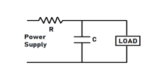
Low pass filter only passes the frequency signal, which is lower than that of the filter’s cutoff frequency. For this low pass filter, the relationship between capacitor resistance and the cutoff frequency is

fc = 1/(2πRC)

The resistor in the circuit is independent of the variation of the applied frequency, but the capacitor is sensitive to the changes in the input signal frequency.
Picture2
Fig. Diagram of first order low pass filter-capacitor circuit.

When the input signal frequency is low, the capacitor’s impedance is higher than the impedance of the resistor to the input voltage drop across the capacitor. Still, when the input signal frequency is high, then the capacitor’s impedance is lower than that of the resistor does more voltage drop across the resistor. Low frequency gets passed through, and high frequency gets blocked.

 In a low pass filter, the frequencies below the cutoff frequency are known as passband, and the frequency above the cutoff frequency is known as stopband.

Low pass filters are used for

  • To reduce electrical noise
  • To limit the bandwidth of the signal
  • To reduce interference

The gain of the low-pass filter in magnitude can be calculated by

Gain of filter = 20log (Vout/Vin)

Vout-> output voltage of the filter

Vin-> input voltage of the filter

Low Pass Filter Capacitor Type

It can be of two type:

  • First Order Filter-Capacitor
  • Second Order Filter-Capacitor

The low pass filter circuit above has only one reactive component capacitor, called one poll filter or first-order filter.

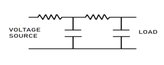
In the second-order of the low pass filter, it has to the reactive element that is capacitor in its circuit does design is helpful when the signal does not provide a wideband range between desired and undesired frequency components.
Picture3
Fig. Diagram of second order low pass filter.

Bypass Filter Capacitor

Here one end of the capacitor is linked to the power supply, and the other is linked directly to the ground. This capacitor helps to reduce the effect of voltage spikes or any AC component from the power supply; it shorts the AC signal to the ground and reduces AC noise to produce a much clear DC signal.
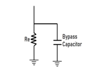
Picture4
Fig. Diagram of Bypass filter Capacitor.

The capacitor in this circuit must have at least one-tenth of resistance as that of the resister Re. As we know, electric current chooses the path with a low resistance to following if it has multiple paths to choose from is; the capacitor offers great resistance to low frequency, so only the AC component of the signal passes through it. The DC component of the input signal will pass through the resistor Re.

High Frequency Filter Capacitor

A high pass filter is a filter that blocks low frequency and let pass through the higher frequency signal here. The frequency lower than the cutoff frequency is blocked, and the frequency higher than the cutoff frequency allowed to pass through this filter is also called a low cut filter. A capacitor is linked in series with the input supply; the resistor is linked in parallel.
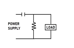
Picture5
Fig. First order high pass capacitor-filter circuit.

 As we know, when the frequency of the input signal is low, the capacitor’s impedance is higher as the capacitor is in series with the power supply through which only a high-frequency signal can pass it.

The above circuit is a first-order high pass capacitor filter as there is only one reactive element in that circuit.

The second-order high pass capacitor-filter and the first order high pass capacitor filter are cascaded together to form a second-order high pass capacitor-filter.
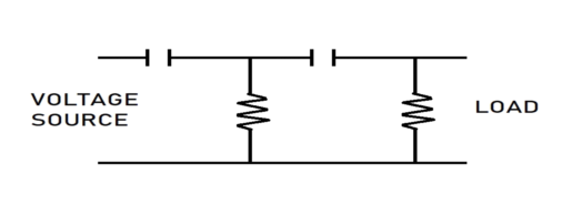
Picture6
Fig. Diagram of Second order high pass capacitor-filter.

3 Terminal Filter Capacitor

Three terminal capacitor-filters consist of a three-terminal capacitor, which features a more negligible impedance than two terminal capacitors. Which allows it to reduce the impedance in the higher frequency band with lesser number of the reactive element it has great noise suppression effect these are used in power lines of circuit, smartphones, LED TV etc.

Harmonic Filter Capacitor

The harmonic filter can be designed of series or parallel reactive elements to block or shunt the harmonic currents. They can be available in several shapes and sizes. Still, when this capacitor is connected in parallel with the power supply, it helps reduce harmonic current and voltage in the circuitry.

The capacitor required in the harmonic filter must accept the given magnitude of various orders of harmonic current. A harmonic current can be a non-sine wave since the capacitor is very sensitive towards the high tension value. The capacitor is used in the harmonic filter in specific ranges depending upon the capacitor in use. A harmonic filter is formed by a capacitor bank, mainly a group of capacitors of the same rating. This filter converts the harmonic current into heat to protect the load from it.

Feedthrough Filter Capacitor

The feedthrough filter-capacitor is a three-terminal capacitor whose grounding impedance is a small and low effect on the lead impedance. It is specially designed for more efficient performance in filtering circuit.

 The ordinary capacitor is not very good for filter application as they have a high impedance which is undesirable and can affect the efficiency of the filtering circuit feedthrough filter capacitor has a small value of shunt capacitance. This capacitor is used in AC and DC supply lines to reduce harmful interference.

The feedthrough filter-capacitor has a filtering effect close to that of an ideal capacitor. The capacitor was initially designed for DC power lines in the RF system, blocking RF energy and letting DC signals pass through it.

Line Filter Capacitor

The line filter capacitor is a capacitor used to suppress electrical noise generated from the power supply.

 The power supply can have various disturbances that include transient surges and fluctuations in its supply voltage. To reduce the effect of such noise, line filter capacitors use line filter capacitors that can endure fluctuations or transients for a more extended period without falling into it.

Line filter capacitor is used to

  • keep potentially damaging line transients
  • To reduce line disturbance produced by the source
  • To reduce the circuit generated noise

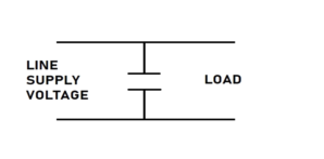
 There are two topologies used in the line filter: one is an X capacitor, and the other is a Y capacitor.

 In X Capacitor, here capacitor is connected across the line supply X capacitor is used where cellular could not lead to an electric shock. It eliminated the electrical noise coming from the power supply and made it used in high-frequency applications. The capacitance of X capacitor can range from 1microF to 10MicroF.
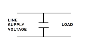
Picture7
Fig. Diagram of X capacitor connected to the power supply.

Y capacitor,  in this topology, capacitors are connected between the line voltage supply and the chassis of the appliances list of colleges used for an application that could lead to electrical shock. The range of this capacitor can be from 0.001 micro F to 1micro F.
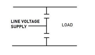
Picture8
Fig.  Diagram of Y filter Capacitor.

Filter Capacitor in a Power Supply Circuit

Picture7 1
Fig. Diagram of X capacitor connected to the power supply.

Alternator Filter Capacitor

Alternator stator windings generate the current 3 phase AC. There is not much ripple voltage to produce radio noise. A diode converts the AC to DC, and if any alternator diode fails, the ripple voltage will increase, or noise can be caused by those who have electrical connections. Still, a filter-capacitor can be used to minimize the noise in the circuit. The filter-capacitor can either block the unwanted AC voltage or bypass the unwanted AC voltage back to the source.

Electrolytic Filter Capacitor

An electrolytic capacitor is a capacitor whose positive plate is made of metal and covered by an insulating oxide layer over the metal. This capacitor uses an electrolyte to have a massive capacitance than other capacitors. The capacitor is used in a filter circuit that combines AC power DC voltage electrolytic capacitor filter to eliminate 60 Hz to 120 Hz AC ripple in DC power supply.

EMI Filter Capacitor

Capacitors used in filtering electromagnetic interference in AC and DC power lines are known as EMI filter capacitors. This capacitor can fail due to over-voltage and transients. There are two different types of topology used in filter capacitor X, and Y.  X capacitor topology is used for differential mode EMI filtering. In contrast, Y capacitor topology is used in standard mode EMI filtering.

Theoretically, several capacitor technologies design X or Y capacitors, but the most commercially available are film capacitors or ceramic capacitors.

Filter Capacitor Design

Filter capacitors can be designed in different ways as per requirement.

 When a low pass filter is created, the capacitor is then connected across the load. When a high pass filter is designed, the filter-capacitor is in series with a power supply. The capacitor-filter is used as a bypass filter when the capacitor is connected between the ground and power supply. Different filter capacitors can be designed based on the different ranges of operations, costs, decisions, operating temperatures and sizes.

Filter Capacitor Amplifier

The filter capacitor has a great disadvantage: the amplitude of the output signal is lower than that of the input signal due to an attenuation of the signal. This means the overall gain of the filter-capacitor is less than one, so there may be a need to amplify the output signal.

 Different amplifiers can be used to restore or control the attenuated signal, such as OpAmp, transistors or FETs. After the capacitor-filter amplifier can draw power from an external source to boost or amplifier the output signal through the capacitor-filter, the output signal of the capacitor-filter can be altered or reshaped as required by the amplifier circuit.

Filter Capacitor Selection

How to select filter capacitor value ?

Select the capacitor-filter based on:

  • Cost
  • Precision
  • Range of operation
  • Stability
  • Leakage current
  • Size
  • Operating temperature

High Voltage Filter Capacitor

High Voltage capacitor passive circuit component that can store charge and energy for use in High Voltage application, ordinary capacitor cannot be used in high voltage applications so high voltage capacitor used in higher voltage range application such as high voltage power line filtering, high voltage AC or DC filtering, high voltage AC or DC bypass, etc. These capacitors are designed where the two metal plates of the capacitor are separated by dielectric metal in between for efficient operation in high voltage application.

How to Test Filter Capacitor

There are two ways to check the filter-capacitor:

  1. Before checking the capacitor, make sure the capacitor is fully discharged. If it is not fully discharged, then discharge the capacitor by connecting it through a load. If you are using a multimeter, then set the metre to read high ohm range. Correctly connect the positive and negative end of the capacitor with the multimeter. The meter should begin from 0 and then move towards infinity, that shows the capacitor is in working condition; if the meter stays at 0, then the capacitor is not charging through the meter, that shows it is not working properly.
  2. Another way to test the filter capacitor, charge the capacitor with the DC voltage supply and then observe the voltage across the anode and cathode of the capacitor. In this test, the capacitor’s polarity is essential just before applying the voltage. Check the capacitor after charging, disconnect the voltage source from the capacitor, and use a multimeter to observe the voltage on the capacitor. Upon checking, the charged capacitor must hold the voltage applied. The voltage will rapidly drop to zero when the multimeter is connected because the capacitor will be discharging through the multimeter. If the capacitor is not holding any value near the applied voltage, then the capacitor is not working correctly.

SMD filter capacitor

SMD stands for surface mounted device which means SMD capacitor is the surface-mounted capacitor nowadays SMD capacitor is widely in use as a filter because they are smaller in size and can be placed easily on the circuit board surface mounted technology allows faster and reliable construction of Electronic element, so it is capacitor are readily available and having cheaper and higher performance.

FAQ

What does a filter capacitor do ?

Filter-capacitors can be used for different purposes with different arrangements in the circuit.

The filter-capacitor can be used to restrict the DC component of the input signal. It can also reject or bypass the AC component of the input signal. Filter-capacitors can limit the signal’s bandwidth or remove a specific range of frequency from the signal. It can also be used to remove unwanted components or noise from the circuitry.

How to select filter capacitors?

Select the capacitor-filter based on:

  • Cost
  • Precision
  • Range of operation
  • Stability
  • Leakage current
  • Size
  • Operating temperature

What is the effect of a capacitor as a filter?

The capacitor is used as a filter. It can filter out AC or DC components from the signal or eliminate a specific frequency range.

Capacitor offers high resistance towards the low-frequency input signal. In contrast, it offers low resistance to the high-frequency signal, so when the capacitor is connected in series with the power signal, only the AC component can pass through that. Only the DC component can passes through the load when the capacitor is linked in parallel to the load.

What are the advantages and disadvantages of capacitor filter?

There are several advantages and disadvantages of capacitor filters.

The advantages of capacitor-filters are cheaper, smaller in size, readily available. The disadvantages of the filter-capacitor are that it is sensitive to temperature change, its capacitance reduces with time.

What happens when filter capacitor value is larger?

The larger the filter-capacitor value, the size of the capacitor also increases with it.

With a larger filter capacitor, the voltage will be minimal. The time constant will be large. The charge will be maintained for a longer period, but it will draw a large amount of current and take a long time to complete the charge and be expensive.

Which one is best either capacitor filter or inductor filter?

The filter can be designed with either a Capacitor or Inductor or by using both.

Capacitor-filters are cheaper than inductor fitters. The size of the filter-capacitor is always less than the size of the inductor filter. The capacitor-filter is better at a smoothening voltage, whereas the inductor filter is better at smoothing current.

Which type of capacitor is used in a low-pass filter?

In a low pass filter, the capacitor is connected across the load.

The type of capacitor used in low pass filter depends on the operating range, temperature, sensitivity, stability, cost, size, etc. The capacitor, which fulfils the requirements, can be used.

What is the difference between a rail and a filter capacitor in a circuit?

A rail capacitor is used in power rail, and the filter capacitor is used for different purposes.

A rail capacitor is used to filter out the noise or ripple in the rail power line. This capacitor is mainly used to maintain the voltage in its rated value and to stabilize it. Where is the filter capacitor used for different purposes such as to eliminate the AC component of the signal, block DC component signal, as bypass filter, EMI filter, limit the bandwidth of the signal, eliminate a specific range of the signal, etc.

Why do we use capacitors as filters in rectification when capacitors are used to block DC and allow AC?

When we use a filter-capacitor in the rectification circuit, it only reduces the AC component of the signal.

In the rectifier circuit, the filter-capacitor is linked in parallel to the load appliances circuit. The DC component of the input signal can pass through the load, and the AC component of the input signal will pass through the filter capacitor. The capacitor shows low resistance towards the high-frequency signal.

What is the effect of filter capacitance magnitudes on the ripple voltage in DC power supplies?

When the filter-capacitor is connected in series with the DC power supply, it reduces the power supply’s AC component.

 A filter-capacitor is used in circuitry to minimize the ripple voltage of the power supply.

The ripple voltage output from the filter can be calculated by 

Vr= Vp/(2fCR)

Where Vr =ripple voltage

Vp = peak voltage

f= frequency of the signal (supply)

C= Capacitance of the Capacitator

R= the value of the resistance
Application of D Flip Flop: 73 Interesting Facts To Know

image 7 1

Shift Register using D flip flop

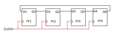
A flip flop is also a single register that can store one bit when a register is designed with multiple flip flops, which can hold more bit data. Finally, a shift register is a type of logic circuit used to store or transfer data.

The shift register is designed with different numbers of flip flops, where data can be conveyed from left to right or right to left. It can have parallel input or serial input and serial output or parallel output. The shift register can also be designed with D flip flops also.

Serial In Serial Out Shift Register using D flip flop

In this type of register, the input is serial one bit at a time, and output is also serial one bit in a serial sequence.

application of d flip flop
Fig. Serial In Serial Out shift register design with D flip flop

Each flip flop can store one bit at a time, so for a 4-bit shift register, four flip flops are needed. As shown above, serial data is applied through D of the 1st Flip flop to all remaining flip flops. When a series of data feeds to the register, each bit is provided to the next flip flop with every positive edge of the clock pulse, and with every clock pulse, the serial data moves from one flip flop to the next flip flop.

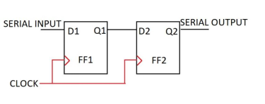
2 Bit Shift Register using D flip flop

The following diagram is the diagram of a 2-bit shift register that can store or transfer 2-bit data. Where input data and output data are both in serial sequence, so it is a Serial in Serial out (SISO) shift register of two-bit, the process of entering data begins with the lowest significant bit of the register, the data input enters the register with every positive edge of the clock pulse.

image 8
Fig. 2 bit shift register using D flip flop

Disadvantages of SISO:

Parallel In Serial Out Shift Register using D flip flop

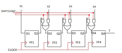
Here are four different data lines for the 4-bit shift register; each D flip flop has its separate input. Data is fed into the respective registers in a parallel way. With every clock pulse, the data bits are shifted towards the output Z. here, and the output comes out in the serial sequence form. Parallel in Serial Out (PISO) shift register can be of two types of data loading: synchronous loading and asynchronous loading. With this shift register, the data in parallel form can be converted into the serial form of data.

image 9
Fig. Circuit diagram of parallel in serial out shift register.

4 bit Bidirectional Shift Register using D flip flop

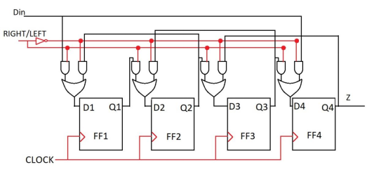
A 4-bit bidirectional shift register is a type of shift register in which data bits can be shifted from left to right or right to left as per requirement. When the Right/Left is high, the circuit works as a right shift register, and when it’s low, this circuit acts as a left shift register, and the data shift with every positive edge of the clock pulse in this type of register.

image 10
Fig. Diagram of 4 bit bidirectional shift register designed with D flip flop

4 bit Universal Shift Register using D flip flop

It is a bidirectional shift register, where input can be fed in serial or parallel ways, and output can also be in serial or parallel. That’s why it is called a universal shift register. Moreover, it can be developed with a D flip-flop, as shown in the given figure of the universal shift register.

image 12
Fig. Circuit diagram of universal register using d flip flop.

8 bit Register D flip flop

The 8-bit register can be designed with an 8 D flip flop.

image 13
Fig. Diagram of 8-bit universal shift register designed with D flip flop

D type flip flop Counter

The counter can be designed with a D flip flop; the number of flip flops depends on the number of bit counters to be developed. In addition, both synchronous and asynchronous counters can be created with the d flip flop.

Counter circuit D flip flop

A counter is a group of flip flops whose state changes with every clock pulse applied. The counter is used to count pulses, form waveform, generate a required sequence, etc.

A counter can be a synchronous or asynchronous counter. The ripple counter is an asynchronous type counter. Several states that counter that pass through before returning to the initial state are called the counter’s modulus.

D flip flop up Counter

The counter starts from the minimum digit value of a counter according to the number of flip flops used to design the counter and goes to the maximum capacity of the counter with every clock pulse. So that is an up counter.

D flip flop Down Counter

The counter starts from the maximum value of the digit according to the number of flip flops used in the counter and goes down to the minimum digit value of the counter. So that’s down the counter.

D flip flop Asynchronous Counter

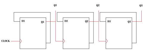
In this type of counter, each Flip Flop has a different clock pulse; the output of this type of counter is independent of a clock pulse; here, the output of a flip flop can be fed into the next flip flop as a clock pulse.

Ripple Counter using D flip flop | Asynchronous D flip flop Counter

Ripple counter, or asynchronous counter, is the simplest form of counter, which is very simple to design and requires very little hardware. However, Flip Flop does not operate simultaneously; each Flip Flop works at different time instances, and each Flip Flop toggles with a clock pulse. Therefore, to design a ripple counter from a d flip flop, the d flip flop must be in a toggle state so that with every clock pulse, it toggles.

4 bit Binary Ripple Counter using D flip flop

image 14
Fig. 4 bit ripple counter designed with D flip flops

3 bit D flip flop Counter Asynchronous Up Counter using d flip flop


image 15
Fig. 3 bit ripple counter which can counter using D flip flop.

2 bit Binary Counter using D flip flop

image 16
Fig. Diagram of 2 bit binary counter designed with D flip flop

3 bit Asynchronous Down Counter using D flip flop

image 17
Fig. Diagram of 3 bit asynchronous down counter designed using D flip flop

Decade Counter using D flip flop

A decade counter is a counter which can count up to 9, the counter starts from 0, and with every clock pulse, it counts up to nine, and when it reaches nine, it resets itself to 0.

image 18
Fig. diagram of decade counter designed using d flip flop

BCD Counter using D flip flop

image 19
Fig. Diagram of BCD counter designed with D flip flop

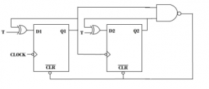
Mod 3 Counter using D flip flop

image 20
Fig. Diagram of mod 3 counter designed with D flip flop

Mod 5 Asynchronous Counter using D flip flop

image 21
Fig. Diagram of mod 5 asynchronous counter designed with D flip flop

Mod 6 Asynchronous Counter using D flip flop

image 22
Fig. Diagram of mod 6 asynchronous counter designed with d flip flop

Mod 7 Counter using D flip flop

image 23
Fig. MOD & counter designed with D flip flop

Ring Counter using D flip flop

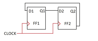
A ring counter is a synchronous counter, where the number is a maximum bit that can be counted depending on the number of flip flops used in the circuit. Here, each flip flop operates simultaneously; the output of a flip flop feeds into the next flip flop as input, where the last flip flop’s output is provided to the first flip flop as input.

Two bit Counter D flip flop   

image 24
Fig. Diagram of 2 bit Synchronous Counter D flip flop

4 bit Ring Counter using D flip flop|4 bit Binary Synchronous Counter with D flip flop

image 25
Fig. 4 bit ring or synchronous counter designed with D flip flop

5 bit Ring Counter using D flip flop

image 26
Fig. Diagram of 5 bit ring counter designed with D flip flop

2 bit Up Down Counter with D flip flops

image 27
Fig.  Diagram of 2 bit up-down counter designed with D flip flop

3 Bit Synchronous Counter using D flip flop

image 28
Fig. Diagram of a 3 bit binary counter designed with D flip flop

3 bit Synchronous Up Down Counter using D flip flop

image 29
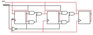
Fig. Diagram of 3 bit synchronous up-down counter  designed with D flip flop.

4 bit Synchronous Up Down Counter using D flip flop

image 30
Fig. Diagram of 4 bit synchronous up counter designed with D flip flop

2 bit Synchronous Counter using D flip flop

image 31
Fig. 2 bit synchronous counter designed with D flip flop.

4 bit Down Counter using D flip flop

image 32
Fig. Diagram of synchronous Down counter designed with D flip flop

4 bit Synchronous Up Counter using D flip flop

image 33
Fig. Diagram of synchronous up counter designed with D flip flop

Design 3 bit Synchronous Counter using D flip flop 

image 34
Fig. Diagram of 3 bit Synchronous counter designed with D flip flop

Johnson Counter Using D flip flop

image 35
Fig. Johnson counter designed with D flip flop

Mod 6 Synchronous Counter using D flip flop

image 36
Fig. MOD 6 counter using D flip flop

Mod 6 Synchronous Counter using D flip flop Truth Table

Q1Q2Q3RESET
0000
0010
0100
0110
1000
1010
1101

Mod 10 Synchronous Counter using D flip flop

image 37
Fig. MOD 10 synchronous counter using D flip flop

Mod 12 Synchronous Counter using D flip flop

image 38
Fig. Mod 12 synchronous counter using D flip flop

Mod 8 Synchronous Counter D flip flop

image 39
Fig. MOD 8 synchronous counter designed using D flip flop

Sequence Generator using D flip flop

A sequence generator is used to generate the required sequence as output; the output set may vary with the requirements, and the series’s length is also very. It can be designed with counters to achieve the required output sequence using different counters with different gates. The sequence generator is used for coding and control.

Pseudo Random Sequence Generator using D flip flop

The pseudo noise sequence is not truly random; it is a periodic binary sequence with finite length to be determined. The PN sequence generator can be designed with a linear feedback shift register, whereas in the shift register, the data is shifted from left to right with each clock cycle.

image 40
Fig. Designing of PN sequence generator using d flip flop

Pseudo noise sequence generator is designed with D flip flop and XOR gate; here the bit got shifted from left to right with clock, the output of the 3rd D flip flop and the output of the 2nd D flip flop are XORed together and feed as input to the 1st D flip flop. The PN sequence increases with the number of flip flops used.

Double Edge Triggered D flip flop

Double Edge or Dual Edge triggered D flip flop is a type of sequential circuit that can select data from the clock pulse’s positive and negative edge. Double edge triggered D flip flop can be designed from two D flip flop one is positive. The other is a negative edge triggered D flip flop connected to a 2:1 multiplexer, wherein the multiplexer clock pulse acts as the select line. The positive edge D flip flop output is fed into one input data, and the negative edge d flip flop output is fed into the other input data of the multiplexer.

image 41
Fig. Double edge triggered D flip flop designed with MUX and D flip flop

Traffic Light Controller using D flip flops

Traffic light controller can be designed with d flip flop, as shown in the given figure, Qbar of the 2nd D flip flop powers the red light. Whereas Q from 1st D flip flop provides power to the Yellow light, the green light gets power when the AND gate is high.

image 42
Fig.  Diagram of traffic light controller designed with D flip flop

Both D flip flops are in toggle states when the clock is high, and the flip flop toggles when there is no clock; the flip flop is in a hold state. The time duration of each light can be controlled with the clock frequency; for different requirements, the clock pulse frequency can be changed.

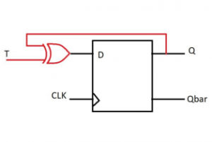
Conversion of T flip flop to D flip flop

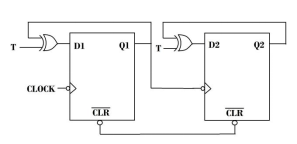
D flip flop can also be designed with a T flip flop when the output of the T flip flop is feed in ]to an XOR gated with Data input, and the output of XOR gate connected to the input of the T flip flop.

image 43
Fig. T to D flip flop conversion

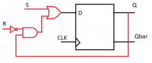
Convert SR Flip Flop to D Flip Flop

Data (D) will be the external input for the flip flop, whereas S and R of SR flip flop are expressed in D, S gets data input, whereas R gets inverted data input.

image 44
Fig. SR flip flop to conversion D flip flop

Conversion of D flip flop to JK

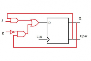
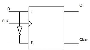
 JK flip flop can be designed with a D flip flop by adding a combinational circuit to the input of the D flip flop, as shown in the given figure.

image 45
Fig. D to JK flip flop conversion
JKQnQn+1D
00000
00111
01000
01100
10011
10111
11011
11100
Table: Conversion table of D to JK flip flop

JK Flip Flop using D Flip Flop and Multiplexer

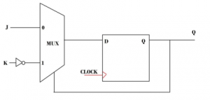
JK flip flops can be designed with a d flip flop and a multiplexer. As shown in the figure, the output Q of the d flip flop is used as a select signal of the multiplexer. Thus, J and K are the input to the multiplexer, whereas J input with an inverter to the multiplexer. The multiplexer used here is 2: 1 MUX; the output of the MUX is acted as the input to the D flip flop as Q changes the select line of the MUX changes accordingly.

image 46
Fig. JK flip flop designed with Multiplexer and D flip flop.

Conversion of D flip flop to T flip flop

The D flip flop should toggle with every high input to convert the D flip flop into a T flip flop. So for that, an XOR gate is connected to the D flip flop, T will be the external input to the XOR gate, and the output of the D flip flop will be the other input of the XOR gate.

image 47
Fig. D to T flip flop conversion

T flip flop using D flip flop Truth Table

DQnQn+1T
0000
0101
1011
1110
Table: D to T flip flop conversion table

D flip flop to SR flip flop

An SR flip flop can be designed with a D flip flop in addition to a combinational circuit, as shown in the given figure. One OR gate AND gate and NOT gates are used to create the additional combinational circuit.

image 48
Fig. D to SR flip flop conversion

D flip flop Toggle Switch

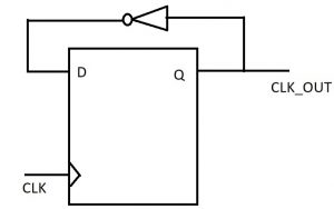
The toggle switch circuit uses a push-button; when the first button press happens, the output will hold into the active, and the output will be held to active or in on state until the next button press happens. I.e., whenever the button is pressed, the output toggles, which can be designed with a D flip flop with a relay switch. D flip flop should be in a toggle state, which can be created by adding the Qbar output of the Flip flop feedback to the D input.

Advantages and Disadvantages of D flip flop

Advantages:

Disadvantages:

D flip flop IC

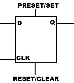
IC stands for an integrated circuit, whereas D flip flop IC means the integrated circuit of D flip flop.D Flip Flop is commercially available in both TTL and CMOS packages format with the majority familiar being the 74LS74 (D flip flop IC) which is a Dual D flip-flop IC, different IC of D flip flops has different IC numbers, and some IC contains eight d flip flops, six d flip flops,  two d flip flops, etc. Moreover, some IC has set and preset pin with the flip flops, some IC has Q compliment as pin output, some IC can contain edge-triggered D flip flops, etc.

File:7474 flip flop.JPG - Wikimedia Commons
Fig. A D flip flop IC 74LS74
Image Credit :  Erwin138 at Hebrew Wikipedia

D flip flop IC number

74HC74, 74LS75, 74HC174, 74HC175, 74HC273, 74HC373, 74HC374A, 74LVC1G79, 74LVC1G74, 74LVC1G175, 74LVC1G80, 74LS74, 7474, CD4013, etc. These are all different types of D flip flop IC.

Single D flip flop IC

A single D flip flop is available on an Integrated circuit. this D flip flop IC contains eight pins, one for data input, one for the clock signal, one for the voltage source, one for ground, one output, one clear, one preset, and one complimentary output Q. It consumes low power and has high noise immunity, and can be packed in any package as it has multiple packaging options. These IC can be used in different applications such as Motor Drives, Telecom Infrastructure, Tests and Measurements, etc.

Single D flip flop IC number

74LVC1G79, 74LVC1G74, 74LVC1G175, 74LVC1G80, SN74LVC1G80, NL17SZ74, NLX1G74, These are some IC number which contains single d flip flop.

Dual D flip flop IC

Two D flip-flops are available in Integrated circuit (IC) form. this D flip flop IC has 14 pins in its integrated circuitry, containing separate input and output for each d flip flops like data input, Q output, and Qbar output in the IC. The remaining pins are two clock pins, one for each flip flop, one voltage supply pin, one ground pin, and two clear pins for both the flip flops. Commercially available dual D flip flop IC are MC74HC74A, MC74HCT74A, CD4013B, SN54ALS874B, SN74ALS874B, HEF4013, 74LS74, 74AHC74D etc. These Dual D flip flop ICs are used in different applications such as time delay circuits, shift register applications, Building Automation, Power Deliver, Telecom Infrastructure, Test and Measurement, etc.

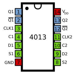
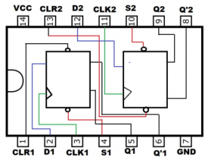
D flip flop Pin Configuration

CLK1, CLK2 -> clock pulse input

VDD -> Voltage supply

GND -> Ground

D1, D2 -> Data input

C1, C2 -> Clear

S1, S2 -> Set

Q2, Q1 -> output

Q’1, Q’2-> complementary output of the flip flop

image 49
Fig. Pin Diagram of D flip flop IC 4013

Dual D flip flop 7474|Dual D type Positive Edge Triggered flip flop

7474 D flip flop IC has two independent D flip flops: positive edge trigger flip flops; the data input is propagated to output Q with the positive-going edge clock pulse. Setup time and hold time of the D flip-flop should be considered for correct operation. Reset and Set in this IC are asynchronous, i.e., both change the output value at any instant of time without considering the clock pulse. The IC 7474 has a wide operating range because of its large voltage range operation.

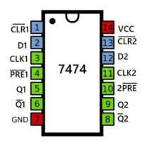
D flip flop 7474 Pin Diagram

image 50
Fig. Pin diagram of D flip flop IC 7474 .

D flip flop IC 7474 Theory

D flip flop IC 7474 is a TTL device. It has data and clock inputs; these inputs are called synchronous because they operate in step with the clock pulse, whereas preset and reset are the asynchronous input. They are independent of the clock pulse. The preset here is active low, where preset is activated with a low input to its pin, it sets the flip flop output Q as 1. The clear signal is also active low; when the clear input is activated, the output Q of the D flip-flop is set to Zero. 7474 D flip flop IC applications are used for Latching devices, Shift Registers, Buffer Circuits, Sampling Circuits, and Memory and Control Registers.

D flip flop IC 7474 Pin Configuration

Pin NumberPin DescriptionInput/Output Pin
1Clear 1Input
2Data 1Input
3Clock 1Input
4Preset 1Input
5Q 1Output
6Q’1Output
7GroundOutput
8Q’2Output
9Q 2Output
10Preset 2Output
11Clock 2Input
12Data 2Input
13Clear 2Input
14Voltage supplyInput
Table: pin configuration of 7474 D flip flop IC.

7474 D flip flop Circuit

image 51
Fig. Circuit diagram of 7474 d flip flop IC.

D flip flop IC 74LS74

74LS74 D flip flop IC has 2 d flip flops; here, every flip flop has different input and output pins; it also has Qbar as an output pin; both flip flops are independent of each other. The Flip Flop here has a positive edge-triggered flip flop with a set preset and clear. 74LVC2G80, HEF40312B are equivalent IC of 74LS74.

Negative Edge Triggered D flip flop IC 

SN74HCS72-Q1 D flip flop IC contains a Dual D type negative edge D flip flop, it has an active-low preset and clear pin, and both are asynchronous. It has 14 pins, one voltage source, two clear, two preset, 2 Q output, 2 Qbar output, one ground, two clocks, 2 data input. Both flip-flops are independent of each other. It is used to toggle switches and can operate in noisy environments. 

74HC74 Dual D Type flip flop

74HC74 D flip flop IC contains dual positive edge-triggered D flip flops and has a total of 14 pins. Two asynchronous reset pins, which are active low, 2 data pins, two clock pins, one ground, two outputs, two complementary outputs, two asynchronous set pins which are active low and one voltage source pin. So it is very high immunity to noise.

74LS74 Dual Positive Edge Triggered D flip flops

74LS74 D flip-flop IC (Integrated Circuit) contains two individualistic positive edge-triggered D flip-flops with asynchronous preset and reset pin. It has 14 pins, two asynchronous reset pic, active low, 2 data pins, two clock pins, one ground, two outputs, two complementary outputs, two asynchronous set pins, and one voltage source pin.

CD4013 Dual D flip flop

The CD4013 or 4013 D flip flop IC is an Integrated circuit containing two d flip-flops; in this IC, you can use 3V to 15V. Some also support up to 20V of power supply. There is a different pin for Data input, Set, Reset, Clock, for both the d flip flop in this IC. And as output, also get Q and Qbar for both the flip flops.

Low Power D flip flop

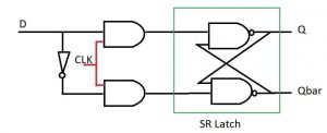
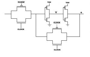
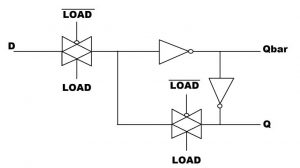
A D flip flop that consumes low power for operation can be designed with AVL (Adoptive voltage level) techniques, TSPC (True single-phase clock) method, or D flip flop designed with transmission gates, which is based on SPTL (Static pass transistor logic) method.

Scan D flip flop

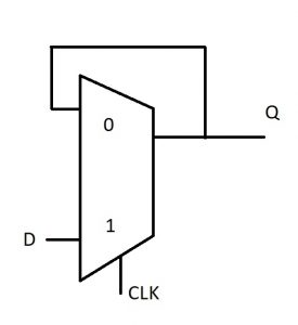
This flip flop has functioned as a simple D flip flop. In addition to that, it has a design for testability. It has scan enable, clock, scan input, and data are the input to a scan d flip flop, enable pin of the flip flop is for it to work as a simple d flip flop or as a scan flip flop. A scan D flip flop is a D flip flop with a multiplexer added to the input where one input of the multiplexer acts as the input data (D) to the D flip flop. This means scan D flip flop is a D flip flop with alternative input sources as per requirement.

TSPC D flip flop

A true single-phase clock d flip flop is a dynamic flip flop type that can perform D flip flop operation with very high speed while using low power, and it also consumes less area. The TSPC method of creating a D flip flop causes minor phase noise in the circuit, which helps to eliminate clock skew.

FAQ/ Short Note

What is the difference between a ring counter and Johnson counter?

Ring counter and Johnson counter are both synchronous counters, there is not much difference between the cirucity of both, here the basic difference between both the counter.

What is the difference between a ring counter and ripple counter?

The ring counter is a synchronous counter, whereas the ripple counter is an asynchronous counter. The difference between both the counters is given below points.

Which counter is faster?

The counter can be of the asynchronous or synchronous counter type. In the synchronous counter, every flip flop receives clock pulse simultaneously, whereas asynchronous counter, every flip flop receives clock pulse at a different time.

The synchronous counter is faster, as all the flip-flops in this counter operate simultaneously. Whereas the speed of the counter depends on the circuitry, type of the flip flop used, clock pulse, delays, etc.

What are the types of shift registers?

The classification of the shift registers into four basic types:

Which shift register is fastest?

There are four different types of shift registers such as SISO, SIPO, PISO, and PIPO. After comparison between all of them, we found out that.

Parallel in and parallel out (PIPO) is the fastest shift register. Here, all inputs and outputs are in parallel form, and the slowest one is the Serial in Serial out (SISO), where all input and output are in sequential format.

What is a mod 8 counter?

Mod is the modulus of the counter which can be number of counter states while counting from minimum to maximum.

Mod 8 counter is a 3 bit counter with 8 states, so it is called mod eight counter. 8 number of input pulses are required to reset this counter to its initial state zero.

What are the application of shift register?

There are several applications for the shift register. Here are some applications for shift register:

What Is Bleeder Resistor: 11 Important Facts You Should Know

filter edited 300x200 1

What is bleed resistor ?

Bleeder Resistor:

This is a standard high-value resistor (connected in parallel with the filter capacitor) used to discharge the capacitor in a filter circuit and primary purpose of using a bleeder resistor in any circuit is safety.

The discharging of the capacitor is very important because even if we turn off the power supply, the charged capacitor can give an electric shock. So it is essential to add a bleed resistor to avoid any mishap.

The function of bleeder resistor:

Let us assume a rectifier with a capacitor filter connected to a power supply. Now, there can be no load present in the circuit, whenever the diode is forward-biased, the capacitor gets charged. As a result, the capacitor produces some voltage across it.

When the diode is reverse biased, the capacitor discharged by a resistor. If the load resistor is not connected, the voltage will be there across the terminals. Now, if we turn off the AC supply, the capacitor still holds some charge. So, if someone touches the terminals, he may get an electric shock. If we can create a discharge path for the capacitor, then We can solve this problem.

Therefore, we connect a highly valued resistor in parallel with the capacitor. This resistor provides a discharge channel for the capacitor. Therefore, it is known as a bleeder resistor.

Bleeder resistor in filter circuit:

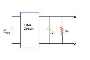
filter edited
Filter Circuit

As we have seen, filter circuits make use of bleeder resistors to ensure safety. Let us think of a simple circuit where a capacitor is attached to the main circuitry. Now once the power supply is ON, the capacitor gets charged. After some time, it reaches the peak value and then starts discharging.

The capacitor remain charged for some seconds after the power supply is OFF. If the capacitor is of very high value, severe problems can happen. First, the capacitor may give a substantial electric shock. Second, if a resistor is connected in parallel, the capacitor gets discharged through this resistor.

How to test a start capacitor with a bleed resistor?

1627906215539
Capacitors in the circuit

Bleed resistor for start capacitor

A capacitor is an energy-storing device. Engineers use this to perform various operations in an electric circuit. First, the capacitor is tested to determine if it is working correctly or not.

When a capacitor is placed in a circuit where the current is flowing, an electric charge builds up on the capacitor plates and after some time, the capacitor accepts no charge, and it means that the capacitor is totally charged. If the circuit requires a charge, the capacitor discharges until the entire charge returns to the circuit.

Following are the steps for testing a start capacitor with a bleed resistor:

  • We short the capacitor terminals using a metal contact.
  • ‌Digital multimeter readings are taken.
  • ‌The power supply is turned on, and we measure how much time the capacitor takes to charge 63.2% of the supply voltage.
  • ‌We calculate the time constant of the capacitor and further determine the capacitance value.

If the voltage rating is the identical or more than the older one, we can say that the start capacitor is working fine.

The bleed resistor on run capacitor:

A run capacitor is a device that optimizes a motor’s performance by adjusting the current and the phase shift. The main difference between a run capacitor and a start capacitor is the first one works continuously, and the second one works in cycles like a switch. As there’s no need for the switch in a run capacitor, the bleed resistor is also unnecessary.

Bleeder resistor design:

A bleeder resistor works when the load resistor is disconnected.

A bleed resistor functions best when it is situated at the 1st capacitor after rectifier, doesn’t draw much current, but it can still cause a volt-drops if connected in series. That’s why the components are connected in parallel.

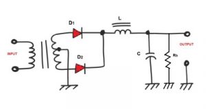
Bleeder resistor circuit:

Bleed resistor circuit

The above rectifier circuit initially consists of an AC power supply, a heavy-duty transformer, two diodes D1 and D2, filter choke L, and filter capacitor C. This capacitor is a large electrolytic capacitor. Therefore, the voltage charging up the capacitor would be very high. However, when we switch the power supply down, a significant voltage still stays for quite some time. So a resistor Rb is connected, which helps in discharging the capacitor.

How to calculate Bleeder resistor value ?

Bleed resistor formula 

The mathematical formula to find bleeder resistance requirement is

Rb = – t/C x ln Vt/Vi

Where C is the capacitance value.

  • t is the time needed for the capacitor to discharge via the bleed resistor.
  • Vt is the voltage up to which the capacitor can be discharged
  • Vi is the initial voltage on the capacitor
  • We cannot exactly specify the value of Vt. However, any low value of Vt serves the purpose.

Treble bleed resistor value

Treble bleed circuits are typically used in guitars. These are standard high-pass circuits that consist of a capacitor soldered to the center and the outside lugs of the volume control. When resistors are used in the treble bleed circuit, they attenuate the high frequencies so that the signal frequency remains balanced. Though there’s no specific information available about the resistor value, it ranges from 120 Kohm to 150 Kohm.

Treble bleed without the resistor

Treble bleed mods are used in some guitars. A resistor might be wired in parallel with a treble bleed or might not be used at all. They can have slightly different effects on the control. However, the tones appear to be the same with or with out the resistor.

Start capacitor bleed down resistor

The bleed-down resistor is the resistor used with the start capacitor. Here “bleed” means to pass. The bleed-down resistor is used to pass off the residual voltage in the start capacitor after removing it from the motor circuit. Though a bleed-down resistor is a safe way, there are other ways to reduce the residual voltage. The resistance value should be somewhere between 10k ohms to 20k Ohms and resistors are generally crimped to the terminals of the start capacitor.

led bleed resistor:

One of the most challenging jobs in LEDs is to improve the dimming of LED lamps in TRIAC dimmers. As these do not have a resistive load, TRIACs intermittently turn off and on and create the flickering effect. This effect degrades the dimming.

To cope up with this issue, LED designers are now introducing bleeding circuits. A small bleed resistor, when used with a capacitor, is called the bleeding circuit. In the LEDs, the bleed resistor is only turned on when needed. Therefore, a trade-off is established, power consumption is lowered, and greater efficiency is attained.

Static bleed resistor:

The bleed resistors are used in Kite antennas for a static build-up. It reduces the voltage observed across the front end of the radio.

Function of bleeder resistor in dc power supply

There are three primary functions of a bleeder resistor.

  • The primary function of a bleed resistor is to provide safety. The capacitor of the filter starts charging when we connect the main supply with the circuit. The capacitor reaches its peak and gradually discharges. Even when the discharging process ends, some excess charge remains in the circuit, and it can give an electric shock to anybody touching the circuit. A bleed resistor connects in parallel help to pass the extra charge thru it.
  • The bleed resistor may act as a voltage divider too. If the equipment is supposed to generate 2 or multiple volt-supplies, the device can be tapped, and the bleed resistor can act as a substitute for the series circuit.
  • Another important use of the bleed resistor is voltage regulation. Mathematically, voltage regulation is the ratio of the diff in between full load and no-load voltage with the full load voltage. As the difference increases, the voltage regulation improves. To attain this, we need to join the bleed resistor in parallel to the filter circuitry and the load resistor, volt-drop occurs in the bleed resistor, this can acts as a voltage regulator too.

SSR bleeder resistor:

SSR refers to the solid-state relays. A solid-state relay is a four-layer switching device that turns OFF and ON if any external voltage is applied across the control terminals.

The leakage current of the SSR circuit on the input side may cause a reset failure. Insertion of a bleed resistor can help prevent this.

 The bleeder resistance value must be set so that the SSR input voltage is a maximum of 0.5 V. when the Relay is OFF.

Reset failure may occur due to solidstate relay leakage current and If this current is higher than the load release current, the solidstate relays may face resetting failure and to increase the Solid-state relay switching current, this resister are adjoined in parallel.

Bleeder resistor tube amp.

The bleeder resistor is not a typical electronic device that is used in everyday gadgets. However, some special equipment like musical instruments, amplifiers contain bleeder circuits. The tube amplifier is such a device. The bleed resistor connected in parallel with the amplifier circuitry easily discharges high voltage capacitors.

ESD bleeder resistor

ESD stands for electrostatic discharge. This discharge might cause damage if not done correctly. So the testing of ESD must be done even it is time-consuming one. Here, the device requires 470 Kohm resistors connected to the ground. The presence of a bleed resistor drastically changes the test results. But the bleeder resistor is needed so that during testing, nobody gets an electric shock.

The most common value for a bleeder resistor

The ratings of the bleeder resistor varies in every circuitry. For example, for a start capacitor AC motor, the value ranges from 10k ohm to 20k ohm. For some other filter circuits, the value can even be more than 200k ohm.

FAQs

What is the bleeder resistor used for?

A bleeder resistor is majorly used in filter circuits to add to the safety and prevent electric shock.

How do I choose a bleeder resistor?

There is always a trade-off between the speed of the bleeder and the total power waste and low values of bleed resistors give a faster time for discharging, but they will give more power loss. We may choose the value with the help of this equation:

Vt = Vie-t/RbC

Where Vt is the instantaneous voltage across the capacitor

Rb is the bleeder resistance

Vi is the initial voltage

t is the instantaneous time period, and C is the capacitance value.

What is a bleed down resistor?

A bleed down resistor is seen in a motor circuit where there’s a built-in start capacitor. The capacitor usually operates for very short instances while the motor is coming up to speed,  if the motor speed up, the capacitor is not required after speeded up. So there should be a switch or voltage sensing device to pull the capacitor out of the circuit. But even after the capacitor is pulled out, for a few seconds, the voltage remains high. It may cause hazards. Therefore a resistor is connected to bleed down the voltage. It is known as a bleed down resistor.

What is bleeder resistance?

This is the resistive value of the bleed resistor in ohm.

How do I select the value of the bleeder resistor to discharge a capacitor at the DC bus automotive inverter application?

The bleeder resistor value should be very high if we want to lower the power consumption when the inverter is kept on. Similarly, the value should be such that the capacitor gets discharged fast.

Why does a DC/DC converter have a bleeder resistor at its output?

The DC/DC converters regulate substantial output capacitance and low load. So, after the device is turned off, there can be a considerable amount of charge left. This charge may take up to several minutes to be discharged and may give a shock to anybody working with it. Therefore, a resistor is attached to the output to fasten this discharging process.

Why do some capacitors have resistors attached to them?

Sometimes capacitors with high value contain resistors so that the stored charge gets drained fast after the power supply is turned off. This resistor provides a discharge channel for the capacitor. Therefore, it is known as a bleeder resistor.

How to use a discharge resistor?

The discharge resistor must be kept in parallel with the circuit so that it can drain the excess charge.

The discharging of the capacitor is very important because even if we turn off the power supply, the charged capacitor can give an electric shock. So it is essential to add a bleed resistor to avoid any mishap.

How do an X rated capacitor and a bleed resistor reduce the voltage in a transformerless power supply?

X rated capacitors have high voltage ratings that can directly be used with AC mains in series. Here the capacitor is used as a voltage divider. Along with the capacitor, the circuit contains a Zener diode and a rectifier with the bleed resistor. The capacitive reactance helps in reducing the voltage.

Why do you need a bleed resistor on the start capacitor?

The start capacitors make use of a bleed resistor to accomplish any task safely after the power supply is turned off.

The function of the bleeder resistor is-

  1. To keep the circuit safe from hazards
  2. To draw high current
  3. To optimize the efficiency of the rectifier
  4. All of the above

Answer: The bleed resistor provides a channel for the capacitor to discharge the remaining charge. Thus it saves the circuit from undesirable accidents.

Which of the following statement(s) is/are true about the bleeder resistors-

  1. The bleeder resistors are connected in parallel with the main circuit
  2. A bleeder resistor prevents the amplifiers from being over-driven
  3. The bleeder resistors can act as voltage regulators
  4. None of the above

Answer: 1 and 3 are correct option. The bleeder resistors are connected in parallel so that they can quickly discharge the capacitor. These can also work as voltage regulators by creating differences between load voltages.

The function of a bleeder resistor in a power supply is

a. To amplify the voltage

b. Discharge the stored charge on the capacitor

c. To increase the output current

d. All of these

Answer: The bleed resistor is used to discharge the capacitor as soon as possible so that no one gets an electric shock while touching the circuit and nothing to do with the current.

How to Calculate bleeder resistor power supply ?

bleed resistor power supply

Let us take a filter circuit connected to an AC supply voltage and has a capacitor with a capacitance value of 2 micro Farad. The initial voltage Vi is 1000 volt, and Vt is 10 volt. The discharging time is 5 seconds, then using the formula, we can calculate the value of the bleed resistor needed to discharge the capacitor.

We know, Rb = -t/[C x ln(Vt/Vi)]

Therefore, Rb = -5/[2 x 10-6 x ln(10/1000)] = 542,888 ohm

Analog Instruments: 23 Important Facts You Should Know

image 40 300x198 1

Content: Analog Instruments

What is Analog Instruments ?

Analog Electronic Instruments

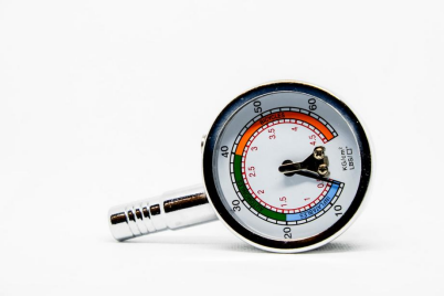
An analog instrument is one whose output or display is a continuous-time function. This instrument converts the input quantity into an analog O/Ps; having an infinite number of value. An analog instrument typically contains a pointer and a scaled calibrated dialler to show the output.

analog instrument
Image Credit :“Detail shot of pressure gauge” by wuestenigel is licensed under CC BY 2.0

Selecting factor of Analog Instrument:

Types of Analog Instruments

The analog instrument can also be of two types:

The direct measuring instrument is the instrument that converts the energy of the measuring quantity directly into energy that trigger the instrument, and the magnitude of quantity to be measured instantly.

A comparison instrument that compares the unknown quantity with a standard, when high accuracy is needed, is used.

One more classification of the analog instrument is

Analog Indicating Instruments

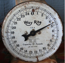
image 39
Image Credit: “Scale Face” by ‘Playingwithbrushes’ is licensed under CC BY 2.0

It is indicating instrument that show the instantaneous value of the magnitude of the quantity to be calculated. The indicating instrument typically includes all null types of instrument and most passive ones. The most used is a dial and a pointer indication by the pointer moving over a calibrated dial.

The analog indicating instrument can be divided into two groups electromechanical instrument and electronic instrument.

Examples are ammeter and voltmeter.

Recording Instruments

The recording instrument gives a continuous record of the variation of the quantity being measured over a specific period. Although it is used to provide the overall performance of any instrument, it can provide data to evaluate the calibre and efficiency of the operating crews.

Types of Recording Instruments

 Analog Recording Instruments can be of three types:

What is Graphic recording instruments ?

Graphic recording instruments display and store records of the history of some physical event with pen and ink. They even may be varying voltage, current, pressure, etc. It mainly consists of a chart for storing and displaying recorded data. This stylus moves on paper with proper relationship and an internal connection which connects the stylus to the information source.

Integrating Instruments

An integrating instrument is an instrument to find the sum of measurements over a specific period the summation in which this provide as product of time and the measured quantity.

Principle of Operation of Analog Instruments

Operating Torques in Analogue Instruments are

421597440 c894109d51 b
Image Credit: “H2: It’s dabom” by jurvetson is licensed under CC BY 2.0

Operating force or torque:

Deflecting Force or torque: It is a force or torque which reflects the pointer from its 0th position of calibrated scale according to the magnitude of the quantity passing thru the device.

Controlling Force or torque:  which control the movement of the pointer on a required scale. It is needed to bring the pointer to the 0th point at if no deflecting force. To produce an equal and opposite force to the deflecting Force to make the pointer steady in the absence of controlling Force pointer may swing away from the final study position for any magnitude. Controlling torque can be produced by Spring control gravity control.

Damping force or Torque: This used to prevent from the vibration for oscillation of the pointer on a particular range of scale; It is required to bring back the pointer at rest. Damping force can be established by air friction fluid friction Eddy current damping.

Magnetic Effect

In a uniform magnetic field, a current-carrying conductor is situated, which result in a disturbance in the magnetic field, impacts force (F). The direction of Force will be the opposite direction of the current and coil conductor generate magnetic field act as magnetic material.

Force of attraction or repulsion 

When a piece of soft iron that is not magnetized previously, kept near the end of the coil. When current flow through the coil, the soft iron becomes magnetised and gets pulled inside the coil. The Force of attraction is proportional to the field strength inside the coil and proportional to the current strength; utilized in attractive moving iron (M.I) instrument.

If two soft iron pieces are situated near the coil, become magnetized, and then there will be repulsion force; utilized in repulsive moving iron (M.I) instrument.

The Force between a current-carrying coil and a permanent magnet is used in a permanent magnet moving coil instrument, and Force among 2 current-carrying coil is utilized as the key principle in dynamo meter type of instrument.

Thermal Effect

The current to be measured is passed through a heating element whose temperature increases with the increase in current and temp change is converted into an EMF by a Thermo-couple. The thermocouple is designed with two dissimilar electric conductors joined together at the end of each other to form a close loop, the point the dissimilar metal meets is the junction. If both the junction is maintained at a different temperature, a current will flow through the loop.

Electrostatic Effect

The electrostatic effect is the attractive force among 2 or many electrically charged elements between which a potential diff is preserved. That force results in to increase in deflecting torque. The electrostatic effect is the basic principle of an electrostatic instrument known as an electrometer voltmeter, an example of an electrostatic instrument.

Advantages of electrostatic instrument:

Disadvantages of electrostatic instruments:

Induction Effect

Induction effect when a non-magnetic conducting disc or drum is placed in the magnetic field which is excited by alternating currents, EMF will be induced in the drum or disc. If the closed path is provided, then EMF will cause a current flow to the drum or disc. the produced force in the interaction of the induced current and the magnetic field will cause the disc or drum to move this effect is used in energy meter.

Advantages of induction instruments:

Disadvantages of induction instrument:

Errors in the induction instrument are due to frequency variation or temperature variation.

Hall Effect

This is the formation of potential difference across a conducting material having electrical current exist in a cross magnetic field.

The magnitude of the potential drop depends on the current flux density, and the internal property of the conductor is called the hall effect coefficient. The emf produced in this phenomenon is so small for measurement, which may require amplification. Hall effect instruments are used for sensing current or in magnetic measurement. Examples are flux meter ammeter Poynting vector watt-meter. Hall effect instruments convert the magnetic field into electric quantity, which can be easily be measured.

Advantages of hall effects:

Disadvantages of hall effects:

What are the advantages of digital instruments over analog instruments?

Advantages and Disadvantages of Analog and Digital Instruments.

Advantages of Digital Instruments over Analog :

Disadvantages of Digital Instrumentation:

Advantages of Analog Instrumentation:

Disadvantages of Analog Instrumentation:

Analog Devices Instrumentation Amplifier

Analog devices instrumentation amplifier when the output of any instrument is low or needed any amplification for further processing the input to the instrument amplifier is the output from the centre of the transducer used to amplify, reject noise and signal interference. An instrumentation amplifier is a differential amplifier, and an analog device instrumentation amplifier is a precision block with a differential input and output. This device amplifies the differences between the two input signal voltages while rejecting signals common to both inputs.

Analog Instrument Cluster |Instrument Cluster Analog

image 40
Image Credit:“Hawker Hunter Cockpit” by G. Weir is licensed under CC BY 2.0

An analog instrument cluster is a group of different analog instruments, and it can include different analog metres and gauges to provide the required measurement. These clusters are used for safety order requirement mainly used in automobiles, aircraft etc. this cluster use different m for measuring required information, for example, in automobile, speed, fuel level, charge level, etc.

What is the difference between Digital and Analog Measuring Instruments ?

Comparison between Analog and Digital instruments

Analog InstrumentDigital Instrument
Low PrecisionHigh Precision
High power RequirementLow Power Requirement
Highly SensitiveLess Sensitive
CheapExpensive
Less ResolutionHigh Resolution
Not compatible directly with a computer, microprocessor or microcontrollercompatible directly with a computer, microprocessor or microcontroller
More FlexibleLimited flexibility
Parallax error during reading result is possibleNo reading error due to digital display
Can get easily affected by noiseHigh noise immune
Easily portableNot easily portable
Continuous convenient for readoutConvenience in readout

Electronic Test Instruments Analog and Digital Measurements

Electronic test instrument testing instruments are used to detect a fault in operation, such as voltmeter, ammeter, ohmmeter, multimeter, frequency counter, oscilloscope or LCR meter, etc.

The testing instrument is the key to any electronic design production and maintenance. It can be an analog or digital instrument used to generate a signal and capture the response from the device Under test.

Analog Aircraft Instruments

Following are the analog instruments which are used in aircraft:

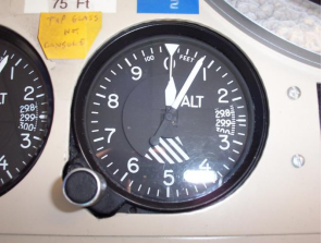
The altimeter is a device used to measure an object’s altitude relative to a fixed level. It has two types of pressure altimeter and radio altimeter and study of altitude is known as altimetry. 

image 41
Image Credit:“Aircraft altimeter” by cambridgebayweather is licensed under CC BY-SA 2.0

A pressure altimeter calculate altitude as per atmospheric pressure. With the increase in altitude, the pressure reduces. Radio altimeter determines the height of any subject by sending a signal to the ground and measure the attitude based on the time required for the radio wave signal to travel. Altimeter having mechanical internal aneroid capsule have an analog display.

Air speed indicator is used to measure the aircraft’s speed; It uses a pitot tube which is U shaped with two openings .airspeed indicator traditionally is a mechanical analog instrument.

Magnetic compass and instrument for determining direction by using a magnetic element which shows the direction of the horizontal component of the magnetic field of the earth

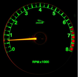
The tachometer is a device that indicates the rate of rotating an object or engine shaft; it includes the instantaneous value of speed in RPM. It is composed of a tile and little to indicate the immediate reading.

image 42
Image Credit: “Jaguar Tachometer” by billjacobus1 is licensed under CC BY 2.0

Analog Polygraph Instrument

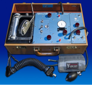
An analog polygraph instrument is commonly known as the Lie Detector instrument, measuring at least three physiological responses like blood pressure, pulse respiration, and skin connectivity.

It can consist of pneumographs to record respiratory activity, blood pressure cliff to record cardiovascular activity,  and galvanometer activity sensor, plethysmograph, etc. The analog polygraph needles draw the line on a paper to record and show the output. These lines represent the level of stress which can affect if the person is telling a lie.

Analog Weather Station Instruments

Analog weather instruments:

The thermometer is used to measure the temperature of the environment. There are many types of thermometers. One of the most used thermometers is a thermistor designed with metal oxide and has a high-temperature Coefficient, so with the temperature change, the resistance shift occurs.

Thermistor mainly has negative temperature Coefficient. Although the increase in temperature resistance decreases, it is very sensitive to temperature change, making thermistors useful for Precision temperature measurement.

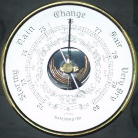
A barometer is an instrument uses to measure the pressure of the atmosphere because atmospheric pressure varies with altitude. A simple barometer is a mercury-in-glass barometer unit of measurement. The atmosphere or bar Mercury glass parameter is closed at the top and open at the bottom. Thus, there is a pool of Mercury. 

image 44
Image Credit :“Barometer” by electricinca is licensed under CC BY-SA 2.0

The aneroid barometer is a non-liquid barometer that is widely in use. It is small and uses an evacuated capsule as a sensing element, the flexible walled evacuated capsule. The flex with the change in atmospheric pressure the deflection is coupled mechanically to an indicating needle.

A hygrometer is a device that indirectly measures humidity by sensing a change in physical or electrical property in materials, which causes due to moisture content. There are different types of hygrometers for humidity measurement. In mechanical hygrometer measures humidity with the change in length of the hair element by the contraction and expansion of the hair element. 

A rain gauge is a device that is used to measure rain in a certain period. It usually measured rainfall in millimetres. There are different types of rain gauges. The most precise one is the ground level gauge, where the orifice of the gauge is placed with the ground level surface and surrounded by an anti-splash grid.

Anemometer is a device that measures the rate of flow, which can be used for measuring airflow. A hot wire anemometer is widely used for measuring the mean and fluctuating velocity of fluid flows. Steam of air will cool down a heated object is the principle of hot wire anemometer a heated wire is placed in the airflow.

Pyranometer is an instrument that is used to measure solar radiation. It is operated on the measurement of the temperature difference between a bright surface and a dark surface. There are different types of pyranometers, such as thermopile pyranometers, photovoltaic pyranometers, etc.

Examples of Analog Instruments

Uncertainty for Analog Instruments

Uncertainty of analogue resolution uncertainty is one of the problems in analogue instruments. It considers the limitation of measurement. The Precision accuracy of a measurement is limited by the resolution of the instrument for an analog instrument with gradual scaling sometimes causes parallax error when taking a reading from different view position will give different reading leads to an error which creates uncertainty in measurement.

Frequently Asked Questions.

What are absolute and secondary instruments?

Absolute Instrument:

These instrument provides the magnitude of the measuring quantity in terms of physical instrumental constant. 

Secondary instrument:

These instrument convert the analog o/ps  of the primary/absolute instrument into an electrical signal. These instruments are required to be calibrated by comparison with an absolute instrument that has already been calibrated.

Analog Instruments are preferred for ?

Error in Analog Instruments ?

three different types of error that happen in any instrument:

  •  Instrumental Errors: These errors are caused by miss-use of the instrument, loading effect, ageing or inherent shortcomings.
  •  Environmental Errors: These errors are caused by external condition of the instrument, hence errors are may affect by surroundings temp, pressure, humidity, dust, etc.
  •  Observational Errors: these errors occur due to human observational factors. There can be reading parallax error in analog instruments, which is an observational error. Different moving parts in an analog instrument can produce an error when friction between two components is created, an instrumental error. Ageing of the instrument can produce an error is also an instrumental error. 

What are some examples of common Analog Devices ?

What are the Comparative Advantages and Disadvantages of Digital and Analogue Multimeters ?

What is a Micrometer ?

Micrometer is also known as micrometer caliper or micrometer screw gauge. It is an instrument for measuring linear(small) distance precisely, such as diameter, length, thickness, etc. 

How does an Ohm Meter Measure Resistance ?

Ohm meter can not measure resistance directly but can measure the power through a circuit. Any known voltage is connected to a component whose resistance is measured, where resistance is unknown by measuring the current through the measuring component. Through Ohm’s Law relationship between voltage current and resistance is known. Therefore, we can calculate the value of the unknown resistance by finding current through the circuit as the voltage is known.

Is Wifi a Digital Signal or an Analog?

The wifi signal is both analog and digital and for that ,  ADC  and DAC and modulation of the signal takes place as requirements.

What is Wattmeter and its construction?

A wattmeter is an instrument that measures the electrical energy of a circuit. The unit of measurement is in watts. It can be an electro-dynamometer or induction watt meter. It can be constructed with a current coil and voltage coil, the current coil is adjoining in series connection, and the voltage coil is connected by parallel connection. The needle which moves on the calibrated scale is connected to the voltage coil. The voltage coil is a moving coil, whereas the current coil is immobile.

How to find Multiplication factor for Wattmeter ?

Multiplication factor = (voltage range X current range X power factor)/(range of wattmeter)

Is there anything that an Analog Multimeter does better than Digital one If so Why ?

Analog multimeters are suitable for measuring fluctuating values better than that of digital multimeters, because sudden fluctuation can not be precisely represented by digital multimeters. While analog multimeter has changing display which can accurately show the sudden fluctuations, it may not provide exact reading but it will provide instantaneous and rough measurement.

D Type Flip Flop : Circuit Diagram, Conversion, Truth Table, Applications

Picture6 300x65 1

What are the different types of a flip flop?

D flip flop Types

Level triggered D flip flop

D flip-flop whose output changes according to the input with a high level of the clock pulse is a level triggered D flip-flop, and then the clock level is low, the D flip-flop stays in a hold state.

What is Edge Triggered D type flip flop ?

D type Edge Triggered flip flop

D edge triggered flip-flop is the flip-flop in which the output can change only with the edge of the clock pulse, regardless of the change in the input. That means the output of the flip-flop changes with the transition of the clock pulse, either from high to low to high. 

D type Edge Triggered flip flop type

Edge triggered D type flip flop can be of 2- types:

The edge triggered flip Flop is also called dynamic triggering flip flop.

Edge Triggered D flip flop with Preset and Clear

Edge Triggered D type flip flop can come with Preset and Clear; preset and Clear both are different inputs to the Flip Flop; both can be synchronous or asynchronous. Synchronous Preset or Clear means that the change caused by this single to the output can affect the clock pulse; here, it is edge triggered to change with the edge of the clock pulse. Whereas Asynchronous Preset can Clear can change the output at any instant of time.

Edge Triggered D flip flop Timing Diagram

The given timing diagram shows one positive type of edge triggered d flip flop; there is clock pulse CLK, D the input to the D flip flop, Q the output of the D flip flop; as you can see, the changes in output are happening during the transition of the clock pulse from low to high, because it is a timing diagram of a positive edged D type flip flop.

Picture6
Fig. Time diagram of a positive edge triggered type d flip flop

Edge Triggered D flip flop Circuit Diagram

The circuit diagram of the edge triggered D type flip flop explained here. First, the D flip-flop is connected to an edge detector circuit, which will detect the negative edge or positive edge of the clock pulse. Then, according to the output of the edge detector circuit, the D flip flop will operate accordingly.

d flip flop types
Fig. Circuit diagram of edge triggered d type flip flop

Edge Triggered D flip flop Truth Table

table 1
Table: Truth table of edge triggered D type flip flop with input and output values.

Rising Edge Triggered D flip flop | Positive Edge D flip flop

The positive edge D type flip flop, which changes its O/P according to the I/P with the +ve transition of the clock pulse of the flip flop, is a positive edge triggered flip-flop. It has high-speed performance with low power consumption, that is because it is widely in use. The positive edge D type flip flop can be represented with a triangle at the D flip-flop block diagram at the clock end. 

Positive Edge Triggered D flip flop Circuit Diagram

The Positive edge triggered D type flip flop circuit can be designed with three latches, where two input latches are adjoining with the clock pulse, one latch is attached with the input data, the circuit is designed in such a way that the output response happens only at positive transition of the clock pulse.

d type flip flop
Fig. Positive edge triggered D type flip flop.

Positive Edge Triggered D flip flop Timing Diagram

Clock pulse CLK, D the input to the D flip flop, Q the output of the D flip-flop, the changes in output is happening during the transition of the clock pulse from low to high.

Picture6 1
Fig. Timing Diagram of +ve edge triggered D flip flop.

Positive Edge Triggered D flip flop Truth Table

table 2 1
Table: Positive Edge Triggered D flip flop Truth Table with input and output value.

Falling edge Triggered D flip flop | Negative Edge Triggered D flip flop

The D flip-flop, which changes its output according to the input with the -ve. transition of the clock pulse of the flip-flop, is a -ve. edge triggered flip-flop. The negative edge D flip-flop can be represented with a triangle and a bubble at the clock end of the D flip-flop block diagram.

Negative Edge Triggered D flip flop Circuit Diagram

The -ve edge D flip flop can be designed by adding a -ve edge detector circuit with the clock pulse. The -ve edge detector detects the -ve edge of the clock pulse. According to the O/P of the detector circuit, the rest of the circuit will operate. When there is a negative transition in the clock pulse, the circuit produces output according to the input. Otherwise, the circuit stays in a hold state.

Picture9
Fig. Circuit diagram of negative edge triggered D flip-flop.

Negative Edge Triggered D flip flop Timing Diagram

Clock pulse CLK, D the input to the D flip flop, Q the output of the D flip flop, the changes in output is happening during the transition of the clock pulse from high to low; this is the characteristic of the negative edge flip flop.

Picture10
Fig. Timing diagram of negative edge triggered D flip-flop

Negative Edge Triggered D flip flop Truth Table

table 3 2
Table: Negative Edge Triggered D flip-flop Truth Table with input and output value.

Master Slave D flip flop | MS D flip flop

Master Slave flip-flop was designed to make synchronization more predictable. To avoid race around conditions, a master slave flip-flop is also known as the pulse-triggered flip Flop because the response time of the output is equal to the width of the one clock pulse.

  Master slave D flip flop can be configured from 2-D flip-flop; each flip-flop is connected to a CLK pulse complementary to each other. One flip-flop as Master and the other act as a slave; when the clock pulse is high, Master operates and slave stays in the hold state, whereas when the clock pulse is low, the slave operates and the Master stays in a hold state. The O/P of the Master is feed into the slave flip-flop as I/P.

How to design Master Slave D flip flop using NAND gates ?

Master Slave D flip flop Circuit Diagram

The master slave D flip flop is designed with NAND gates, configured with 2-D flip-flops, one a latch with the gated circuit, as a master flip-flop, and the other work as a slave flip-flop with a complemented CLK pulse to each other.

Picture11
Fig. Circuit diagram of Master Slave D flip-flop designed with NAND gate.

Master Slave D flip flop Truth Table

DQ(PREVIOUS)CLOCKQ
0010
0110
1011
1111
0000
0101
1000
1101
Table: Master salve D flip-flop Truth Table with input and output value.

Timing Diagram of Master Slave D flip flop

In the given diagram, a signal of the CLK pulse, D the I/P to the master flip-flop, Qm is the O/P of the master flip-flop, and Q is the O/P of the slave flip flop. Thus, the behavior of a master slave D flip-flop can be observed through its timing-diagram.

Picture12
Fig. Timing Diagram of the Master-Slave D flip-flop.

Master Slave Edge Triggered D flip flop

If the master slave circuit is designed with edge triggered D flip flop, or in addition to D flip-flop circuit, there is one edge detector circuit, which detects the edge of a clock pulse. According to the output of the detector, the Flip-flop works. Then the overall circuit is a master slave edge triggered flip flop circuit.

D flip flop Design

D flip flop can be configured in many ways, like it can be created with NAND gate, NOR gate, Multiplexer, etc. It can be derived from other flip flops like JK flip flop, SR flip flop, or T flip flop. It can be designed with the help of many different combinations of the circuit with the clock.

How to design D flip flop using NAND gate ?

D flip flop circuit diagram using NAND gates

The D flip flop can be designed with NAND gate only, here one SR latch is designed with NAND is gated with two more NAND gates, and the clock pulse is input to the gated NAND with Data input, where one NAND gate D as input and the other NAND gate gets D compliment as one input. And according to the gated output, the SR latch is processed. The resulting circuit is a D flip flop circuit.

Picture13
Fig. D flip flop circuit designed with NAND gates

How to design D flip flop using NOR gate ?

D flip flop using NOR gate

The D flip flop can also be designed with NOR gates; here, three SR latches with clock pulse are used to develop the D flip-flop. The two input SR latch create the D and D complement output separately, and that output is feed into the third latch, which produces Q and Q-compliment as output. 

Picture14
Fig . Circuit Diagram of D flip flop designed with NOR gates

When there is no clock pulse, the initial latches get locked with the current state because of the interconnections, which cause the whole flip Flop to put on a hold state; regardless of the change in input data, the output cannot change.

D flip flop using 2 D Latches

Picture5
Image Credit :jjbeard, Public domain, via Wikimedia Commons

Transparent latch D flip flop

Picture16
Image Creditr:Glpuga – Author’s own work., Public Domain,

What is D flip flop SR Latch circuit diagram ?

Picture17
Fig. D flip-flop designed with SR latch

How to design D flip flop Using CMOS ?

D flip flop using CMOS Transistors


Picture18
Fig. D flip flop CMOS circuit designed with PMOS and NMOS.

Design D flip flop using Transmission Gate

The D flip flop can be designed with a Transmission gate, which reduces the complexity of the circuit as it reduces the number of transistor counts. When LOAD =0, the Latch stores the data input; when LOAD = 1, the latch is transparent. The transmission gate also helps to reduce the overall circuit size.

CMOS D flip flop Schematic

Picture19
Fig. Schematic diagram of D flip flop designed with Transmission gates.

D flip flop using 2×1 MUX

Picture21
Fig. D flip flop designed with a multiplexer (MUX).

D flip flop using MUX Explanation

A D flip flop can be designed with a single multiplexer(MUX), data ‘D’ is an input to the MUX, and the other input of the MUX is the feedback of the multiplexer output Q to itself’s input, the clock signal is acting as select line, If the clock (CLK) = one then the output of the MUX is D, otherwise the output of the MUX remain the past output Q. 

How to Design D flip flop using JK flip flop ?

Conversion of JK flip flop to D flip flop

D will be the external input to the JK flip flop, and JK flip flop is the universal flip Flop; we can design D flip-flop from the JK flip flop if we connect the K input of the JK flip flop with an inverter to the J input. Then the resulting circuit will be D flip-flop with I/P as D and O/P as Q and Qbar.

Picture22
Fig. Block representation of D flip flop designed from JK flip flop.
Inputoutput
JK flip inputflop

DQnQn+1JK0000X010X11011X111X0

Table: Conversion table from Jk flip flop to D flip flop with input and output values.

Where Qn+1 means the next output state and Qn means the present output state in the conversion table.

How to design Frequency Divider Circuit using D flip flop ?

D type flip flop Frequency Divider | D flip flop Clock Divider

A frequency divider is a digital circuit that divides an input frequency by a required factor. One such frequency divider is designed with a D flip flop, which divides the input clock frequency by two. One inverted feedback is from output Q to the input D is forming this frequency divider circuit.

Picture4
Fig. Frequency divider circuit designed with D flip flop and NOR gate.

Divide by 3 Circuit using D flip flop

The given circuit divides the input frequency by three. In this circuit there is 2 D flip-flop is used, and one NOR gate, which forms the resulting circuit, divides the input frequency by three.

Picture3
Fig. Frequency divider circuit designed with D flip flop which divide the frequency by 3.

Phase Detector using D flip flop

A phase frequency detector is a circuit used to detect the difference of frequencies and phase of two given inputs. The UP signal is generated when the clock signal is slower than the reference clock signals. The down signal is generated when the clock signal is faster than the reference clock.

Picture2
Fig. Phase frequency detector using two D flip flops.

The phase frequency detector can be designed with two D flip-flop as shown in the above figure; both the flip flop has different clock frequencies as input, and the reset of the flip flops are connected with a NAND gate whose input is the Down and Up signal.

Frequency Multiplier using D flip flop

The frequency multiplier is a digital circuit that generated the multiple of the input clock frequency signal. 

Picture1 2
Fig. Frequency multiplier designed with D flip-flop and inverters.

The circuit can be designed with the D flip-flop and even the number of inverted in the feedback line. The feedback is started from the output Q and goes to the NOR gate, which is attached with the clock input of the Flip Flop. The multiplier circuit output depends on the delay produced by the inverters; with different delays, we can produce different frequencies as output.

D flip flop Oscillator

The oscillator is a circuit that generates repeated and alternating waveforms. The oscillator can be designed with D flip-flop, where D flip-flop must be in a toggle, so whenever it gets a high input, the output value should toggle; for creating toggle flip flop from d flip flop, the complementary output of the D flip-flop is feedback to the Data input of the D flip-flop.

D flip flop Register

A register is a group of flip flops that can store more than one bit at a time, depending on the number of flip flops in the register.

What are the Quad D flip flop IC ?

Quad D type flip flop 74175 | Quad D flip flop 7475

Quad d flip flop is available in Ingratiated circuitry, which has 16 pins. It has a 4 d flip flop with separate input(D) and output ( Q and Qbar ) pins. The remaining pins are one ground, one clear, one clock, and one voltage supply pin. Its function is equivalent to the TTL 74175. It contains edge triggered D flip flop.

Hex D type flip flop

It is a type of d flip flop available in IC, which contains 6 d flip flops each has different input and output pin in the integrated circuit. Thus, it has 16 pins with one clock pin, one ground pin, one voltage supply pin, and one clear pin.

8 bit Octal D flip flop

Octal d type flip flop is commercially available as an Ingratiated circuit. It contains 20 pins, which have three-state output. All the flip-flops are mainly controllable by the clock and enable pin. Each flip Flop has different input (D) and output (Q) pins. The remaining pins are one clock pin, one ground pin, one voltage supply pin, one clear pin. This Ic is used to design a storage register, pattern generator, etc.

16 bit D flip flop

 It is a type of D flip flop available in IC; mainly a 16-bit edge triggered d flip flop with three-state output, designed for driving highly capacitive or low impedance load. It can be used as a 16 bit flip Flop, also can be used as two 8 bit flip flops. It has 48 pins, whereas each flip Flop has separate pins for input and output; two clock pins and two enable pins. It is used in designing buffer registers, input or output ports, bidirectional buses, etc.

Exhaustive Vhdl Code & Verilog Code: 27 Important Facts

vhdl code verilog code 0

 Content :

Verilog was originally for stimulation and verification of digital circuits, it is a hardware description language (HDL). Here, all the code is designed with D flip flop whether VHDL or Verilog code.

Verilog Code for D flip flop using NAND gates

module nand_g(c, a, b); //*each module contains statements that defines the circuit, this module defies a NAND gate which is named as nand_g*//

input a, b; / a and b is the input variable to the NAND gate
output c; / output variable of NAND gate is defined
assign c = ~(a & b); / this assign is used to derive the value of c through a and b
endmodule /module end with endmodule statement

module not_g(e, f); / this block defines the NOT gate
input f; / f is the input variable to the NOT gate
output e; / e is the output variable of the NOT gate
assign e = ~f;
endmodule

module d_ff_st(q_out, qbar_out, d_in, clk_in );
 //* this module defines a d flip flop which will be design with NAND gate and NOT gate *//
input d_in, clk_in; / input variable of D flip flop d_in is the data input and clk_in is the clock input 
output q_out, qbar_out; / output of the D flip flop q_out and qbar_out where q_out and qbar_out is compliment to each other

not_g  not_1(dbar, d_in); /NOT gate module is called with dbar and d_in parameter

nand_g nand_1(x, clk_in, d_in); /NAND gate module is called with x, clk_in and d_in parameter
nand_g nand_2(y, clk_in, dbar); /NAND gate module is called with y, clk_in and dbar parameter
nand_g nand_3(q_out, qbar_out, y); / NAND gate module is called
nand_g nand_4(qbar_out, q_out, x); / NAND agte module is called
endmodule

Verilog Code for D flip flop with Asynchronous Reset

module dflip_flop_asy_rst (q, d_in, clk_in, reset_in);

input d_in, clk_in, reset_in; / input variables  of the d flip flop is defined
output reg q; / output variable of the d flip flop is defined
always@ (posedge clk_in or posedge reset_in) 

//* always block is the block who's statements are executed sequentially here the block will executed when clk_in is in positive edge or reset_in is in positive edge *//

if (reset_in) / if reset_in is high or true then q <= 1'b0 
q <= 1’b0; / here 1'b0 means one bit number value zero
else / if reset_in is low or false then q<= d_in
q<=d_in;
endmodule / end of the module
verilog
fig. Block diagram of D flip flop designed from the above Verilog code.

Verilog Code for D flip flop using Dataflow Modelling

//* 
Dataflow modeling provides the descriptions of combinational circuits by their function rather
than by their gate structure.*//

module dflipflo (q, d_in, clk_in); / module defines d flip flop in data flow modelling

input clk_in, d_in ; / input variable of the d flip flop

output q; / output variable of the d flip flop

assign q = clk_in ? d_in : q; / if clk_in is true the q = d_in and if clk_in is flase the q = q

endmodule
d ffff
Fig. Diagram of d flip flop designed with the above dataflow code.

D flip flop Behavioral Verilog Code

//* Behavional is used when cicruit is sequential circuit it contain procedural statements *//
module dflip_flop_bh (q, d_in, clk_in); 

input d_in, clk_in; / input variable of d flip flop is defined
output reg q; / output variable of the d flip flop is defined

always @ (posedge clk_in) / the block is takes place continuously when clk_in is in its positive edge of the pulse

if(clk_in) / if clk_in is high or true then q<=d_in
q<=d_in;
endmodule

Verilog Code for Shift Register using D flip flop

//* this code is used to designed 4 bit shift register using d flip flop, here left to right shifting is taking place through this code*//
module shift_reg_LtoR (out, clock, reset_in, in);/ this module define left to right shift register of 4 bit

input in, clock, reset_in; / input variable is defined
output out;
output reg [3:0] s; / output varible s is defined as a register that can have 4 bit value

always@ (posedge clock, negedge reset_in) 
//* the sensitivity of this block is negative edge of reset_in or positive edge of clock *//
\t
if(!reset_in) / if else statement
s<=4’d0;
else
s<={ s [ 2 :0], in}; //* as s can have 4 bit value the s[2 : 0] has 3 bit and in has 1 bit, together they produce the 4 bit of s *// 
assign out= s[3];
endmodule

4 bit Ripple Counter using D flip flop Verilog Code

//* following code is for 4 bit ripple counter designed with d flip flop*//
module dff_r (input d_in, clk_in, rst_in, output reg q, output q_n); 
//* module define a d flip flop with clock, reset, d, as input, and q and qbar as output *// 

always@(posedge clk_in or negedge rst_in) //* this block sensitivity is positive edge of clk_in pulse or negative edge of rst_in *// 

if (! rst_in) / if rst_in is low or false the q is implemented with zero
q<=0;
else
q<= d_in;
assign 
 q_n <= ~q;
endmodule

module ripple_c (input clk_in, rst_in, output [3:0] o); / this module define the ripple counter of 4 bit
wire q_0, qn_0, q_1, qn_1, q_2, qn_2, q_3, qn_3; / wire is used to define the output or input signal 

 //* implementing d flip flop module with different parameter 4 times *//
dff_r dff_0(.d_in(qn_0), .clik_in(clk_in), .rst_in(rst_in), .q(q_0), .q_n(qn_0));
dff_r dff_1(.d_in(qn_1), .clik_in(q_0), .rst_in(rst_in), .q(q_1), .q_n(qn_1));
dff_r dff_2(.d_in(qn_2), .clik_in(q_1), .rst_in(rst_in), .q(q_2), .q_n(qn_2));
dff_r dff_3(.d_in(qn_3), .clik_in(q_2), .rst_in(rst_in), .q(q_3), .q_n(qn_3));

assign o={qn_0, qn_1, qn_2, qn_3};

endmodule

Positive Edge Triggered D flip flop Verilog Code

module pos_edge_df (q, d_in, clk_in, rst_in);
 //* this module define d flip flop with q as output and data, clock and reset as input *//

input d_in, clk_in, rst_in; / input variable of the d flip flop is defined
output reg q; / output variable of the d flip flop is defined

always @ (posedge clk_in) / this block is implemented continuously with every positive edge of the clock pulse

if ( !rst_in) / if else statement
q<= 1’b0;
else
q<=d_in;

endmodule
0000 1 edited 1
fig. Block diagram of D flip flop designed from the above code.

Negative Edge Triggered D flip flop Verilog Code

module pos_edge_df (q, d_in, clk_in, rst_in);  
//* this module define d flip flop with q as output and data, clock and reset as input *//

input d_in, clk_in, rst_in; / input variable of the d flip flop is defined
output reg q; / output variable of the d flip flop is defined

always @ (negedge clk_in) / this block is implemented continuously with every negative edge of the clock pulse

if ( !rst_in) / if else statement
q<= 1’b0;
else
q<=d_in;

endmodule

Verilog Code for D flip flop using Structural Model

/Structural model is used to integrate diffrenet blocks

module nand_gat(co, a, b); / this module defines NAND gate
input a, b; 
output co; 
assign co = ~( a & b); 
endmodule

module not_gat(e, f); / this module defines NOT gate
input f; 
output e; 
assign e= ~f; 
endmodule

module d_ff_strt(q,q_bar,d_in,clk_in); //* this module define d flip flop with q and qbar as output, and data and clock as input *//
input d_in, clk_in; / input variable of the d flip flop is defined
output q, q_bar; / output variable of the d flip flop is defined

not_gat not1 (d_bar, d_in); / here NOT gate module is implemented

/ next NAND gate module is implemented with different parameters 4 times
nand_gat nand1 (x, clk_in, d_in); 
nand_gat nand2 (y, clk_in, d_bar); 
nand_gat nand3 (q, q_bar, y); 
nand_gat nand4 (q_bar, q, x); 

endmodule

Verilog Code for Ring Counter using D flip flop

module dffc (q_in, d_in, clk_in); / d flip flop module is defined
output reg q_o;
input d_in,c_in;
initial
q_o=1'b1;

always@(posedge clk_in) / sensitivity is positive edge of the clock pulse
q_o = d_in;
endmodule

module ring_counterdff (q_o, clk_in); / ring counter module is defined with d flip flop
inout [3:0]q_o;
input clk_in;

/ d flip flop module is implemented with different parameters 4 times
dffc df1(q_o[0], q_o[3], clk_in);
dffc df2(q_o[1], q_o[0], clk_in);
dffc df3(q_o[2], q_o[1], clk_in);
dffc df4(q_o[3], q_o[2], clk_in);
endmodule

Verilog Code for T flip flop using D flip flop

module T_ff(q, t_in, clk_in, rst_in); / this module define T flip flop 

input t_in, clk_in, rst_in; / input variable of the t flip flop is defined
output q; / output variable of the t flip flop is defined

always @ (posedge clk_in) / sensitivity of this block is positive edge of the clock pulse
if(rst_in)
t_in<=t_in^q;
endmodule

D flip flop Verilog Code with Testbench

//* following code is the test bench for a d flip flop is does not have any input or the output as variable, it's purposes is of exercising and verifying the functional correctness of the hardware model *//
module d_flipflopt_b;

reg d_in;
reg clk_in;
wire q;

d_flipflop_mod uut (.q(q),.d_in(d_in), .clk_in(clk_in) );
initial begin
d_in = 0;
clk_in = 0;
end

always #3 clk_in=~clk_in;
always #5 d_in=~d_in;
initial                     #100 $stop;

endmodule

Master Slave D flip flop Verilog Code

module M_slave(d_in, reset_in,clk_in, q ,q_bar);/ this module define the master slave of d flip flop
 input d_in, clk_in ,reset_in;
 output q, q_bar; 
 Master Maste_r(d_in, reset_in, clk_in, qn, q_barn); / implementing master d flip flop module 
 Master Slav_e(q_n,reset_in,!clk_in,q, q_bar); / implementing slave d flip flop module
endmodule

module Master(d_in, reset_in, clk_in, q_in, q_bar); / this module defines d flip flop
 input d_in, reset_in, clk_in;
 output reg q, q_bar;
 initial
  q = 0;
 
always @(posedge clk_in) begin
  if (~reset_in) begin
   q <= d_in;
   q_bar <= !d_in;
  end
  
else begin
   q <= 1'bx;
   q_bar <= 1'bx;
 end

 end

endmodule

JK flip flop using D flip flop Verilog Code

module D_flip_flopf (input D_in ,clk_in ,Reset_in, enable_in,  output reg Fo); / this module define D flip flop
    always @(posedge clk_in) begin
        if (Reset_in)
            Fo <= 1'b0;
        else if (enable) 
            Fo <= D_in;
    end 
endmodule

module JK_flip_flopf (input J_in, K_in ,clk_in, Reset_in, enable_in, output Q); / this module defines JK flip flop
    wire S_1,S_2,S_3,S_4,S_5;
    D_flip_flopf D1(S_4, clk_in, Reset_in,enable_in, Q );

    not N2(S_5, Q);
    and A1(S_1, J_in ,S_5);
    not N1(S_3, K_in);
    and A2(S_2,S_3,Q);
    or O1(S_4,S_1,S_2);
endmodule

Frequency Divider using D flip flop Verilog Code

module freq_div_by2 (clk_out, clk_in, reset_in); //* this module defines frequency divider which can devide the frequency by 2 *//
input clk_in, reset_in;
output reg clk_out;
always @ (posedge clk_in)
if(reset_in)
clk_out<=0;
else clk_out<=~clk_out;
endmodule
FRQ DIV D FF edited
fig. Block diagram of the frequency divider circuit designed with D flip flop.

D flip flop Verilog Code Gate Level

module dffgate(D_in, CLK_in, Q ,Q_n);
    input D_in, CLK_in;
    output Q, Q_n;
    reg Q, Q_n, Ro, So;

always @(negedge CLK_in) begin
    Ro = ~(~(~(D_in|So)|Ro)|CLK_in);
    So = ~(~(D_in|So)|Ro|CLK_in); 
    Q = ~(Ro|Q_n);
    Q_n = ~(So|Q);
end
endmodule

Image Credit : “Binary code” by Christiaan Colen is licensed under CC BY-SA 2.0

VHDL Code for D flip flop

library ieee;
use ieee.std_logic_1164.all;

entity d_flip_flop is 
port (d_in, clk_in: in std_logic; q, q_bar: out std_logic);
end d_flip_flop;

architecture beh_v of d_flip _flop is 
signal qn, q_barn: std_logic;
begin
Process (d_in, clk_in)
begin
If (clk_in’ event and clk_in = ‘1’)
then qn <=d_in;
end if;
End process;
q<=qn;
q_bar<=not (qn);
end beh_v;

VHDL Code for D flip flop using Dataflow Modelling

library ieee;
use ieee.std_logic_1164.all;
use ieee.std_logic_arith.all;
use ieee.std_logic_unsigned.all;

entity d_flip_flop is 
port (d_in, clk_in: in std_logic; q_in, q_out: inout std_logic);
end d_flip_flop;

architecture data_f of d_flip_flop is
signal d_1, s_1, r_1: std_logic;
begin
s_1 <= d_in nand clk_in;
d_1 <= d_in nand d_in;
r_1 <= d_1 nand clk_in;
q_in <= s_1 nand q_out;
q_out <= r_1 nand q_in;
end data_f;

VHDL Code for D flip flop using Structural Model

library ieee;
use ieee.std_logic_1164.all;
use ieee.std_logic_arith.all;
use ieee.std_logic_unsigned.all;
entity d_f _f_st is 
port (d_in, clk_in: in std_logic; q_in, q_out: inout std_logic);
end d_f_f_st;

architecture d_ff_s of d_f_f_st is
component nand_1
port (a, b : in std_logic; c : out std_logic);
begin

n_0: nand_1 port map(d_in, clk_in, s_1);
n_1: nand_1 port map(d_in, d_in, d_1);
n_2: nand_1 port map(d_1, clk_in, r_1);
n_3: nand_1 port map(s_1, q_out, q_in);
n_4: nand_1 port map(r_1, q_in, q_out);
end d_ff_s;

library ieee;
use ieee.std_logic_1164.all;
use ieee.std_logic_arith.all;
use ieee.std_logic_unsigned.all;

entity nand_1 is
port (a, b: in std_logic; c: out std_logic);
end nand_1;

architecture beha_v of nand 1 is 
begin
c<= a nand b;
end beha_v;

D flip flop Behavioral VHDL code

library ieee;
use ieee.std_logic_1164.all;
use ieee.std_logic_arith.all;
use ieee.std_logic_unsigned.all;

entity d_flip_flop_bh is
port (d_in, clk_in, rst_in: in std_logic; q_in, q_out: out std_logic);
end d_flipflop_bh;

architecture beh_v of d_flip_flop_bh is 
begin
process(d_in, clk_in, rst_in)
begin
If (rst_in = ‘1’) then q_in <= ‘0’;
else if (rising_edge(clk_in)) then q_in <= d_in;
q_out<= not d_in;
end if;
end process;
end beh_v;

VHDL Code for D flip flop with Asynchronous Reset

library ieee;
use ieee.std_logic_1164.all;

entity d_ff_asy_rst is
port (d_in, clk_in, reset_in: in std_logic; q_out: out std_logic);
end d_ff_asy_rst;

architecture beha_v of d_ff_asy_rest is 
begin
if (reset_in = ‘0’) then q_out<=’0’;
elseif (clk_in’ event and clk_in= ‘1’)
then
q_out<=d_in;
end if;
end process;
end beha_v;

VHDL Code for D flip flop with Synchronous Reset

library ieee;
use ieee.std_logic_1164.all;

entity d_syn_reset
port( d_in, reset_in, clk_in: in std_logic; q_out: out std_logic);
end d_syn_reset;

architecture beha_v of d_syn_reset is
begin
process
begin
wait until (clk_in’ event and clk_in =’1’)
if reset_in = ‘0’ then q_out<=’0’;
else
q_out<= d_in;
end if;
end process;
end beha_v;

VHDL Code for Negative Edge Triggered D flip flop

library ieee;
use ieee.std_logic_1164.all;

entity d_ff_neg is
port (d_in, clk_in: in std_logic; q_out: out std_logic);
end d_ff_neg;

architecture beha_v of d_ff_neg is
begin process (clk_in) begin
if (clk_in’ event and clk_in = ‘0’) then
q_out<= d_in;
end if;
end process;
end beha_v; 

Test Bench for D flip flop in VHDL

library ieee;
use ieee.std_logic_1164.all;

entity d_flip_flop_test is
end d_flip_flop_test;

architecture behaviour of d_flip_flop_test is
component d_flip_flop_test
port( d_in: in std_logic; clk_in : in std_logic; rst_in: in std_logic; d_out: out std_logic);
end component;
signal d_in: std_logic:= ‘0’;
signal clk_in : std_logic:= ‘0’;
signal rst_in: std_logic:= ‘1’;
signal d_out: std_logic;
constant clk_p: time:=20ns;
begin 
uut: d_flip_flop_test
port map(d_in=>d_in; clk_in => clk_in; rst_in=> rst_in; d_out=> d_out);
clk_p: process begin
clk_in<=10;
wait for clk_p/2;
clk_in<=’1’;
wait for clk_p/2;
end process;
sti_prc: process
begin
rst_in<=’1’;
wait for 50 ns;
rst_in<= ‘0’;
d_in <= ‘0’;
wait for 50ns;
rst_in<=’0’;
d_in<= ‘1’;
wait;
end process;
end;

4 bit Shift Register using D flip flop VHDL Code

library ieee;
use ieee.std_logic_1164.all;
 
entity p_I_p_o is
 port(
 Clk_in: in std_logic;
 D_in: in std_logic_vector(3 downto 0);
 Q_1: out std_logic_vector(3 downto 0)
 );
end p_I_p_o;

architecture archi of p_I_p_o is
begin
 process (clk)
 begin
 if (CLK_in'event and CLK_in='1') then
 Q_1 <= D_in;
 end if;
 end process;
end archi;

VHDL Code for 8 bit Register using D flip flop

library ieee;
use ieee.std_logic_1164.all;

entity reg_sip_o is
port (clk_in, clear : in std_logic; input_d : in std_logic; q: out std_logic vector (7 downto 0 ) );
end reg_sip_o;

architecture arch of reg_sip_o is 
begin
process (clk_in)
If clear = ‘1’ then 
q<= “00000000”;
 elseif (clk_in’ event and clk_in = ’1’ ) then
q(7 downto 1)<= q(2 downto 0);
q(0)<= input_d;
end if;
end process;
end arch;

VHDL Code for Asynchronous Counter using D flip flop

//*following is the VHDl code for a asynchoronous counter designed with d flip flop *//
library ieee;
use ieee.std_logic_1164.all;

entity dff1 is
port (d_in, clk_in ,clr_in : in std_logic; q, q_bar : inout std_logic);
end dff1;

architecture my_dffbharch of dffl is
begin
process (d_in, clk_in, clr_in)
begin
if (clr_in  = '1') then
if (clk_in  = '1') AND (clk_in'EVENT)  then
q <= d_in;
q_bar <= not (d_in);
end if;
else
q <= '0';
q_bar <= '1';
end if;
end process;
end my_dffbharch;

library IEEE;
use IEEE.STD_LOGIC_1164.ALL;

entity dcoun is
port(clk_in, clr_in :in std_logic;
q, q_b:inout std_logic_vector(3 downto 0));
end dcoun;

architecture arch of dcoun is
component dff1 is
port(d_in, clk_in, clr_in :in std_logic;
qi, q_bar:out std_logic);
end component;
signal k ,p , m :std_logic;
begin
k<=qi (0);
p<=qi (1);
m<=qi (2);
a1:dff1 port map('1','1', rst_in, clk_in , qi(0),q_b(0));
a2:dff1 port map('1','1', rst_in,k,q(1),q_b(1));
a3:dff1 port map('1','1', rst_in, p, qi(2), q_b(2));
a4:dff1 port map('1','1', rst_in, m,qi(3), q_b(3));
end arch;

What is a Power Triangle: 23 Facts You Should Know

Power trinagle 300x200 1

The triangle of power | Power voltage current triangle

A power triangle is simply a rightangle triangle with side representing active power, reactive power, and apparent power. The base component symbolizes active power, the perpendicular component denotes reactive power, and the hypotenuse symbolizes apparent power.

What is power triangle?

Define power triangle | Power triangle definition

A power triangle is the graphical presentation of real or active power, reactive power, and apparent power in a right-angled triangle.

Power triangle equation | PQS power triangle

Power triangle

Power triangle formula calculation | Power triangle equation

In a power triangle, active power P, reactive power Q, and apparent power S form a right-angled triangle. Therefore,

hypotenuse2 = base2 + perpendicular2

S2 = P2 + Q2

Here, Apparent power(S) is measured in Volt-Ampere(VA).

Active power(P) is measured in Watt(W).

Reactive power(Q) is measured in Volt-Ampere reactive(VAR).

  • A power triangle is the graphical presentation of real or active power, reactive power, and apparent power in a right-angled triangle.
  • Active or true power refers to the entire amount of power dissipated in an electrical circuit. It is measured in Watt (W) or KiloWatt (KW) and represented with P and average value of the active power P.
  • Reactive power or imaginary power is the power that doesn’t do any real work and causes zero power dissipation. T is also known as watt-less power. This is the power derived from reactive elements like the inductive load and the capacitive load. The reactive power is calculated in KiloVolt Amp reactive (KVAR) and is denoted by Q.
  • The total power in the circuit, both absorbed and dissipated, is known as apparent power. The apparent power is computed by multiplying the r.m.s voltage with r.m.s current without any phase angle quantity.
  • Ohm’s Law always works with DC circuits, but in the case of AC, it only works when the circuit is purely resistive, i.e., the circuit doesn’t have any inductive or capacitive load. But, most of the AC circuits consist of a series or parallel combination of RLC. Due to this, voltage and current become out of phase, and a complex quantity is introduced.
  • The power of the three-phase system is = √3 x power factor x voltage x current.

Power triangle for RLC series circuit | Power triangle circuits

RLC

Let us consider an RLC circuit connected in series as above.

Where, a resistor with resistance R.

 an inductor with inductance L.

a capacitor with capacitance C.

An AC voltage source Vmsin⍵t is applied.

V is the r.m.s value of applied voltage, and I is the r.m.s value of the total current in the circuit. The inductor and the capacitor produce XL and XC oppositions, respectively, in the circuit. Now, there can be three cases-

Case 1: XL > XC

Case 2: XL < XC

The power triangle is obtained from the phasor diagram, if we multiply each of the voltage phasors with I, we get three power components.

Phasor

From the phasor triangle, we can quickly get the power triangle by multiplying the voltages with I. The real power is multiplied by VR, which is equal to I2R. The reactive power is I multiplied by (VC – VL), which is equal to I2(XC – XL). The apparent power V = I2Z is calculated from the active power and the reactive power for both cases, Here we take into consideration another quantity, the complex power. The complex power is the summation of the active power and the reactive power represented in complex form, i.e., with the ‘j’ quantity.

Therefore, complex power

S = P – jQ  when XL < XC

S = P + jQ when XL > XC

Now, for case 1, inductive reactance is less than capacitive reactance. Therefore, reactive power is negative, and angle ϕ is also negative. For case 2, inductive reactance value is more than capacitive reactance value, reactive power is +ve, and angle ϕ is also +ve.

Active reactive apparent power triangle | Power volts amps triangle

Active power and reactive power triangle.

True power triangle.

Active or true power refers to the entire amount of power dissipated in an electrical circuit. It is measured in Watt (W) or KiloWatt (KW) and represented with P and average value of the active power P is,

P = VI = I2R

Reactive power triangle

Reactive power or imaginary power is the power that doesn’t do any real work and causes zero power dissipation. Itt is also known as watt-less power. This is the power derived from reactive elements like the inductive load and the capacitive load. The reactive power is calculated in Kilovolt Amp reactive (KVAR) and is denoted by Q.

Reactive power Q = VIreactive = I2X.

Apparent power triangle

The total power in the circuit, both absorbed and dissipated, is known as apparent power. The apparent power is computed by multiplying the r.m.s voltage with r.m.s current without any phase angle quantity.

Apparent power

CodeCogsEqn 27

For a purely resistive circuit, there’s no reactive power. So, the apparent power is equal to active or true power.

Power triangle for AC circuit | Electrical power triangle

AC circuits can have any combination of R, L, and C and if we want to calculate the total power correctly, we have to know the phase-diff among the I and V. The waveform of the current and the voltage are sinusoidal. As the power = voltage x current, maximum power is obtained when both the waveforms coincide. In this situation, the waveform are called ‘in-phase’ with each other.

  • In a purely resistive AC circuitry, the I and V perfectly align with each other in terms of phase. Therefore just by multiplying them, we can get the power.
  • If the circuit has any inductive or capacitive load, a phase difference is created. Even if the phase difference is minute, AC power is divided into two parts- one positive and one negative. The negative power is not a mathematically negative quantity; it just implies that the power is provided to the system, but no energy transfer takes place. This power is known as reactive power. The positive quantity does some real work, so it is classified as real or active power.
  • Another portion of power is provided to the circuit from the source. It is known as apparent power. The apparent power is calculated by multiplying the r.m.s values of the current and the voltage.

Ohm’s Law power triangle | Ohm’s power triangle

Ohm’s Law always works with DC circuits, but in the case of AC, it only works when the circuit is purely resistive, i.e., the circuit doesn’t have any inductive or capacitive load. But, most of the AC circuits consist of a series or parallel combination of RLC. Due to this, voltage and current become out of phase, and a complex quantity is introduced. We need to apply some special formulas in order to calculate the alternating current and parameters of the power triangle.

Power triangle for capacitive load

A capacitive load means that the power factor is leading as the current lead the voltage by the phase angle.

Power triangle for inductive load

An inductive load represent that the power factor is lagging because the I lags V by the phase angle.

Complex power triangle

Complex power is nothing but the representation of power using complex numbers. The real part represent the active power. Imaginary part represent the reactive power.

Let us assume that the current and the voltage in a capacitive circuit are I and V, respectively. We know, for capacitive load, the I leads the V by a phase angle. Let us take this angle as ϕ.

Let’s say the voltage across the load, V= ve and current I = iej(Ɵ+ϕ).

We know, the power is the voltage multiplied by the current conjugate.

So complex power S = VI* = ve x ie-j(Ɵ+ϕ)= vie-jϕ

S = vi(cosϕ – jsinϕ) = vicosϕ – jvisinϕ = P – jQ [we know active power P = vicosϕ and reactive power Q = visinϕ ]

For the capacitive load, the I lags V by the phaseangle. So, the voltage across the load, V= ve and current I = iej(Ɵ-ϕ).

So complex power

S = VI* = ve x ie-j(Ɵ-ϕ)= vie

S = vi(cosϕ + jsinϕ) = vicosϕ + jvisinϕ = P + jQ

Three-phase power triangle

Alternating current can be single-phase or three-phase. The variation of current amplitude results in the generation of sine waves. For a single-phase supply, there’s just one wave. Three-phase systems split the current into three parts. The three current components are out-of-phase by one-third of a cycle each. Each current component is equal in size but opposite in direction to the another two conjunctive.

The power of the three-phase system is = √3 x power factor x voltage x current.

Impedance triangle and power triangle

Impedance triangle power factor

In DC circuits, only the resistance is responsible for opposing the current. But in AC circuits, a quantity called reactance also opposes the current. The reactance can be any combination of inductance and capacitance. But both the inductance and the capacitance differ from the resistance with a phase angle (lagging or leading). So, we cannot add them arithmetically. So, we construct an impedance triangle with hypotenuse Z(impedance), base R(resistance), and reactance X( inductive or capacitive reactance or both).

CodeCogsEqn 28

Power factor= R/Z

Power triangle power factor

The power factor in the power triangle is referred to as the ratio of active power and apparent power, defined as the cosine of the phasor angle.

Power factor correction triangle

The power factor correction is a method to increase the efficiency of an electrical circuit by reducing the reactive power. Power factor correction is achieved through parallel-connected capacitors that oppose the effects caused by inductive elements and decrease phase shift.

Power factor triangle formula

The power factor for capacitive or inductive load= R/Z

Power factor = Real power/Apparent power

Power energy triangle

Electrical energy is defined as the system’s power multiplied by the total time the power is used.

Energy E = P x T

How to draw a power triangle?

Power triangle generator

The power triangle is constructed by taking the active power as the base, the reactive power as perpendicular, and the apparent power as the hypotenuse.

Metal triangles on power lines

We often see a few triangular loops hanging from the power lines. These are used to provide stability to the lines in high wind. These triangular fins prevent the lines from bouncing too close to each other and ensure that they are not loosened from the insulators.

Electrical power triangle calculations | Power triangle calculator

Q. An inductor coil of 120 mH and a 70 ohm resistance are connected in series with a 220 volt, 50 Hz supply. Calculate the apparent power.

Inductive reactance

CodeCogsEqn 29

Impedance of the inductor

CodeCogsEqn 30

So, the current consumed by the inductor = V/Z= 220/79.5 = 2.77 A

Therefore, phase angle

CodeCogsEqn 31

lagging

Active power

CodeCogsEqn 32

Reactive power

CodeCogsEqn 33

Apparent power

CodeCogsEqn 34

Q. Calculate the power factor of the series RLC circuit with inductive load 23 ohm, capacitive load 18 ohms, and resistive load 12 ohms connected with a 100 volt 60 Hz supply voltage.

Given:

Inductive reactance XL = 23 ohm

Capacitive reactance XC = 18 ohm

Resistance = 12 ohm

Total impedance of the circuit

Power factor of the circuit = R/Z = 12/13 = 0.92

Power triangle example

Q. A load of 20 kW is at a power factor 0.8 lagging. Find the capacitor rating so that it can raise the value of the power factor to 0.95.

Here, the true power P = 20 KW

Power factor cosϕ1 = 0.8

We know, the reactive power must be reduced to get an increased power factor. Therefore, the phase angle will also decrease. Let us assume that initially, the phase angle was ϕ1, and after reducing the reactive power, the phase angle is ϕ2. So, the power triangle looks like-

Example

We can see from the diagram that the reactive power has decreased to AB from AC. So we need to compute the difference of AC and AB, and this quantity is the required capacitor rating.

Here, OA = 20 KW

cosϕ1 = 0.8

cosϕ2 = 0.95

We know, cosϕ1 = OA/OC  

So, OC = 20/0.8 = 25 KVA

AC = √(OC2 – OA2) = 15 KVAR

Cosϕ2 = OA/OB

So, OB = 20/0.95 = 21 KVA

AB = √(OB2 – OA2) = 6.4 KVAR

Therefore, BC = AC – AB = (15 – 6.4) = 8.6 KVAR

FAQs

How many types of powers are there in the power triangle?

The power triangle consists of three types of power

  • – True or active power.
  • – reactive power.
  • – apparent power.

What is power triangle? Explain active,reactive and apparent power with an exemplar.

The power triangle is the triangular representation of the relationship between the true power, the reactive power, and the apparent power.

For example, in any electrical appliance, the total power generated is the parts of the active and the reactive power.

What is the power triangle of an AC circuit?

The power triangle of an AC circuit can be resistive, capacitive, or Inductive and  triangle consists of three kinds of powers, and the apparent power is computed with the help of the active power and the reactive power.

What is the power triangle of an RL circuit?

The RL circuit has a power triangle with the active power = I2R, the reactive power = I2XL, and the apparent power = I2Z, where XL is the Inductive reactance and Z is the total impedance of the circuit.

What is the relation between KVA, KW, & KVAr?

KVA is the unit of the apparent power, whereas KW and KVAR are the units of true power and reactive power, respectively. Therefore from the concept of the power triangle, we can conclude that KVA2 = KW2 + KVAR2.

What is the significance of the power factor?

For inductive and capacitive loads, the power factor plays a vital role in computing the reactive power. Reactive power is the part of active power that gets diminished and powerfactor is the ratio of the true power and the apparent power. The unity power factor indicate that the circuit is completely resistive in nature.

How many watts is 6 KVA?

6 KVA = 6000 VA

At unity power factor 6 KVA = 1 x 6000 = 6000 Watts

If the power factor is anything else, 6 KVA = 6 x (power factor) watts

How to convert KWH to KVAH?

KWH = KVAH X power factor

Therefore, KVAH = KWH/ power factor

How many watts does 1 kVA equal to?

For a purely resistive load, there’s no reactive power. So the power factor is 1. Here 1 kVA= 1 Watt

If the load is capacitive or inductive, the resistive power is not 0, as power factor is resistance/impedance. Here 1 kVA = power factor x 1 KW

Why are electric towers in triangular shapes?

For the following reasons, electric towers are triangular.

  • ‌Triangles have a greater base area which allows them to be highly rigid. This rigidity helps in withstanding side loadings.
  • ‌Triangles have less area than any quadrilateral. If the shape were quadrilateral, then the cost would have been more. The triangular shape reduces the cost by eliminating one extra side.

What is the power factor for a transformer?

The power factor of a transformer depends upon the characteristics of the load.

‌If the load is purely resistive, the power factor is Unity or 1.

‌If the load is capacitive, i.e., XC > XL, the power factor is known as leading.

‌If the load is inductive, i.e., XL > XC, the power factor is known as lagging.

What is the difference between KVA KWH KVAH and KVAR? | Power triangle KW KVA KVAR

KVA stands for Kilo Volt Ampere. This is the unit of real or active power.

KWH stands for Kilo Watt Hour. This is used to measure how much power(in kilowatts) is consumed in an hour.

KVAH stands for Kilo Volt Ampere Hour. KVAH is the apparent power, whereas KWH is the active power. KVAH = KWH/ power factor

KVAR stands for Kilo Volt Ampere reactive. It is used to measure reactive power.

What is the power factor of an L-R circuit?

The impedance of an L-R circuit is Z = R + jωL

We know, power factor

CodeCogsEqn 36
CodeCogsEqn 37

What is the unit of the power factor?

The power factor is the ratio of the active power (KW) and the apparent power (KVA) as both the numerator and the denominator are powers, the power factor is a unit less quantity.


Kelvin 4 Wire Resistance Measurement: 11 Important Facts

circuit 2 1 300x284 1

The Subject of Discussion: Kelvin 4 Wire Resistance Measurement:

What is 4 Wire Resistance Measurement ?

4 Wire Resistance Measurement

There are different methods to measure different types of resistance, where varies with the range of resistance. 4 wire resistance measurement method is a very accurate measurement method, which can measure very low resistance with high accuracy. It is used to avoid contact resistance or lead wire resistance problems in the circuit. Here every connection wire is called kelvin connection.

In 4 wire resistance measurement method, the four-wire connection is used where two-wire is used to deliver the supply current to the measuring component, and another two-wire is used to measure the voltage drop across the measuring element.

As we know, at constant temperature Ohm’s law define resistance ‘R’ as the ratio of voltage across the resistance to the current ‘I’ passing thru it, So with measuring the voltage drop across the measuring component with known current passing through it, the resistance of the measuring element can be calculated.

What is Kelvin Bridge ?

Kelvin Bridge

The basic principle of the Kelvin 4 wire resistance measurement is based on Kelvin Bridge. Kelvin Bridge is a modified version of the Wheatstone bridge used to measure the very low resistance value, which ranges from 1 ohm to 0.00001 ohms. In this bridge, the effect of load resistance contact resistance and the resistance of the lead wires are taken into account.

Kelvin Bridge Circuit:

circuit 3
Fig. Kelvin Bridge circuit.

Yb in the figure is the connecting lead wire Resistance.

Whenever the galvanometer is connected to point ‘a’, then the resistance of the connected lead is summed up to the resistance Rx and total impacts become Rx + R{ab} + R{cb}.

Whenever the meter is attached  to point ’c’ the resistance of the lead wires  summed up to R3 + R{ab} + R{cb}.

And when the galvanometer is attached to the point ‘b’, which is between ‘a’ and ‘c’ point, in such a way that the ratio of lead resistance from ‘a’ to ‘b’ and ‘c’ to ‘b’ is the same as the ratio of R1 to R2.

Equation 1 :

ezgif 2 b3fb185b26

Now the overall equation of the circuit become

Equation 2 :

ezgif 2 91861ae3f0

From equation 1 and 2 after solving we get :

ezgif 2 bcad55c4b3

The final equation is the same as the balanced Wheatstone Bridge, which shows that connecting lead wire has been eliminated by connecting the galvanometer at point ‘b’. Yb is eliminated with the kelvin bridge.

Kelvin 4 Wire Resistance Measurement has been described in this article with important concepts .
4 Wire Resistance Measurement Circuit elaborated.
Advantages and Disadvantages of Kelvin 4 Wire Resistance Measurements described.
Difference between 4 Wire vs 2 Wire Resistance Measurement represented.
Important Applications of 4 Wire Resistance Measurement has been described.

*************************

What is 4 Wire Resistance Measurement ?

4 Wire Resistance Measurement Method | 4 Wire Resistance Measurement Technique

When measuring low resistance, the connecting wires can cause an error in the result of measurement. If the error produced is higher than the tolerance, or if the accuracy of the measurement is required very high degree, then four-wire resistance measurement is used. Ideally, the wire does not have any internal resistance, but in practice, every wire has some internal resistance.

4 Wire Resistance Measurement Circuit:

In the 4 wire resistance measurement method, 4 wire connection is used where two-wire is used to deliver the measurement current to the measuring component, and another two-wire is used to measure the voltage drop across the measuring component.

kelvin 4 wire resistance measurement
Fig. 4 wire resistance measurement circuit.

In this 4 wire resistance measurement method fixed current generator is used. So if the resistance through the circuit varies, the fixed current generator will supply a constant current through the circuit.

The wire which is used in voltage measurement is connected straight to the legs of the resistance, which is to be measured, and the voltage metre is used in this method is of high impedance so that minimal current passes through it. With a small current through the wire, the overall voltage drop across the wire is negligible, which doesn’t affect the value of the measuring component voltage drop. This method eliminates the wire resistance, which is also called Kelvin or four-wire method. Hear special connecting clips are used, which is known as Kelvin clips.

Kelvin Clip Circuit Connection:

circuit 4
Fig. Kelvin Clip used in the circuit connection.

Kelvin clips are also known as alligator or crocodile clips. Each half of the jaw of a Kelvin clip is insulated from one another; both Jaws of the Kelvin clip are electrically common to each other, which usually joint at the high point. The current delivering wire is connected to one jaw, and the voltage measuring wire is linked to the other jaw. Kelvin Clips are used when the accuracy of the measurement is required high.

What are the Applications of 4 Wire Resistance Measurement ?

4 Wire Resistance Measurement Application:

  • Remote Sensing.
  • Resistance thermometer detector.
  • Induction hardening.

What are the main Disadvantages of  4 Wire Resistance Measurements ?

Disadvantages of Kelvin 4 Wire Resistance Measurements:

  • Expensive.
  • Complicated circuit.
  • Testing speed is very slow.
  • The no. of test points is twice.
  • Larger number of connection wires are required.

2 Wire and 4 wire Resistance Measurement

In the 2 wire resistance measurement, the total lead wire resistance adds to the measurement because the current through the whole circuit is the same. As the voltage drop through the wire and the measuring component can produce a measurement with error, It does not have a very accurate output for a small value of resistance when the measuring resistance is much larger than the wire resistance. Then the lead resistance can get negligible. If the length of the wire can be minimum as possible, then the measurement’s accuracy can be increased.

circuit 1 1
Fig. Two wire resistance measurement connection.

As we can see from the above figure, RW1 and RW2 are the lead wire resistance. This is because the Voltmeter measures the voltage drop across R + RW1 + RW2 . 2 wire resistance measurement is a less accurate simple circuit structure, requiring fewer connecting wires.

3 Wire Resistance Measurement

3 wire resistance measurement, which is not accurate as 4 wire resistance measurement, is more accurate than two-wire resistance measurement. The complexity of the circuit is less than that of 4 wire resistance measurement.

circuit 2
Fig. 3 wire resistance measurement circuit.

In this method, the switch is used, so at first, the upper loop of the resistance is measured, the Voltmeter measures the voltage across RW1 + RW2, then divide the value by 2, which gives the average resistance of these two wires. RW3 is assumed to be the same as the avg. of RW1 and RW2.
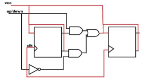
Then, switch the circuit to the regular connection, which measures the measuring component and the resistance of wire RW2 + RW3. The calculated value across ( R + RW2 + RW3) then compared with the first measured value

ezgif 2 31d0940e12

which is used to eliminate the lead resistance produced by the wire from the measured value.

3 wire resistance measurement connection can be very accurate if all the three wires connected are of the same resistance value R1 = R2 = R3. 3 wire resistance measurement is widely used in industrial applications, which offers good compromise; it is accurate and uses less wire than 4 wire resistance measurement.

4 Wire Resistance Measurement Vs 2 Wire | 2 Wire Vs 4 Wire Resistance Measurement | 4 Wire vs 2 Wire Resistance Measurement

Parameter4 Wire Resistance Measurement2 Wire Resistance Measurement
Connecting wire4 connection wire2 connecting wire
AccuracyVery high even for low resistance measurement.Very low for low resistance measurement.
Used for range of the resistanceUnder 1-ohm resistance1 ohm to 1 kilo ohm
Circuit designComplexSimple
CostExpensiveCheap
Table: comparison between kelvin 2 wire and kelvin 4 wire resistance measurement

Frequently Asked Questions

What is actual working of 2 wire 3 wire and 4 wire types of resistance temperature detector i e RTD ?

RTD stands for resistance temperature detector. It is known that the resistance of a metal changes with the temperature change, so by measuring the resistance with the temperature change, the temperature difference can be detected. They are some metals where the temperature Coefficient is positive, so with the increase in temperature, the electrical resistance of metal increases. RTD can use 2 wire, 3 wire or 4 wire method.
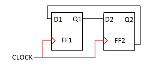
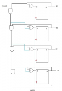
The error introduced by the lead can cause a significant error, so there are very few applications of 2 wire RTD, 2 wire RTD is used with short lead wire or where high accuracy is not needed. Three-wire RTD measurement circuit that minimises the effect of lead wire resistance as long as the connecting wires are of the same length. Some factors such as terminal corrosion or loose connection can still significantly differentiate the lead resistance.
Three-wire RTD is more accurate than two-wire RTD, whereas less accurate than 4 wire RTD, where three-wire RTD is commonly used in the industry relatively cheaper than that of four wires and has a more straightforward Circuit Design than that of a four-wire RTD. In 4-wire resistance measuring, RTD is where the lead wire resistance can be observed and separate from the sensor measurement 4-wire RTD is a true 4 wire resistance measuring Bridge 4-wire RTD is used where high accuracy is needed. Still, it is very expensive and complex in design.
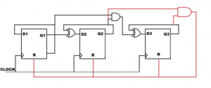
What are the disadvantages of the method of measuring resistance of a wire utilizing an ammeter and a voltmeter in a circuitry ?

Disadvantages depend upon the circuitry’s design, which will measure the resistance for two-wire resistance measurement accuracy is low and for four-wire resistance measurement accuracy is high. In contrast, the two-wire measurement circuit is very simple and cheap, whereas 4 wire resistance measurement is complex and expensive.
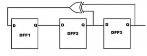
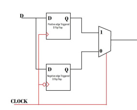
The disadvantage of measuring resistance using an ammeter and Voltmeter can be using meters that are not working correctly. The range of the measurement should be considered for the selection of meters, other disadvantage voltmeter and ammeter should be connected to the circuit in different branches. The Voltmeter should be connected parallel to the measuring load, where the ammeter should be connected in series with the branch where the current is to be measured.
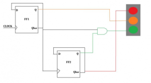
To know more about mutual inductance click here
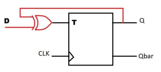
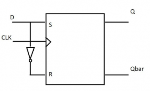
What is the resistance of an electric heater?
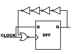
According to Joule heating or Ohm heating, heat is proportional to resistance. Joule heating is a process by which electric current passes through a conductor produces heat, so for an electric heater, there must be high resistance in the wire.

What are the factors affecting the resistance?

  • Temperature
  • Length of the wire area
  • Cross-section area the wire
  • Nature of material

Will a thick wire have more resistance than a thin wire Why ?

The thin wire usually have greater resistance than a thick wire because the thin wire has fewer electrons to carry the current and In comparison, the thick wire has more electrons to carry the current. In addition, the relation of resistance and area of cross section of a wire is reciprocally proportionate, because of this if cross section of a wire reduce, the value of wire’s resistance will be higher.

How to increase the resistance of a wire ?

The increase in length of the wire or decrease in the area of the cross-section of a wire increases the resistance.

What is the cross sectional area of a wire?

If we cut a wire vertically perpendicular to its length, then we get a circle face of the wire. The area of the circle face of the wire is known as the cross sectional area of the wire and this area of a wire does not depend upon the length of the wire, and it is generally uniform throughout the entire length of the wire.

Why use a high impedance voltmeter ?

Ideal Voltmeter has an infinite impedance that does not consume any current from the circuit. Still, practically e infinite impedance is not possible. A high impedance voltmeter is used. The current that passes through the Voltmeter is very small, so it does not affect the overall circuit.

Is temperature is directly proportional to resistance ? 

The temperature is directly proportional to resistance for a metal conductor or the metal with a positive temperature coefficient.

What are the effects of temperature on resistance?

The effect of temperature on resistance depends on the temp co-efficient of the resistance. This can be defined as the change in resistance per unit change in temperature,if co-efficient is positive, resistance will increase with the temperature rise and if Co-efficient is negative, resistance will decrease with the temperature rise.

Can a wire have zero resistance?

Ideally, zero wire resistance is possible, but practically, no wire present has zero resistance.
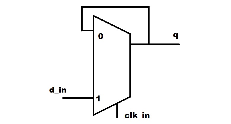
Why do we use three-wire RTD?

Three-wire RTD is most accurate when connecting lead wire resistance to three-wire RTD is cheaper than a four-wire RTD and has a less complicated Circuit Design than a four-wire RTD.

What is the benefit of a four-wire resistance measurement?

Four wire resistance measurements can eliminate the lead wire resistance and have resistance measurement having the highest accuracy.
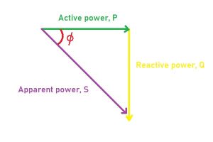
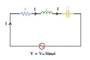
Link to latest article

Mutual Inductance Transformer: 17 Important Concepts

CodeCogsEqn 45 convert.io

Mutual inductance is a fundamental concept in the field of electromagnetism. It refers to the phenomenon where a changing current in one coil induces a voltage in another nearby coil. This occurs due to the magnetic field produced by the first coil, which cuts across the turns of the second coil, resulting in the generation of an electromotive force. Mutual inductance plays a crucial role in various applications, including transformers, inductors, and wireless power transfer systems. Understanding mutual inductance is essential for designing efficient and reliable electrical circuits.

Key Takeaways

Mutual Inductance
– Induced voltage in one coil due to a changing current in another coil
– Occurs due to the magnetic field produced by the first coil
– Essential for transformers, inductors, and wireless power transfer systems

Understanding Mutual Inductance

Mutual inductance is a fundamental concept in the field of electromagnetic induction, which is governed by Faraday’s law. It describes the interaction between two coils or inductors that are in close proximity to each other. This phenomenon occurs when the magnetic field generated by one coil induces a voltage in the other coil. Mutual inductance plays a crucial role in various electrical circuits and devices, such as transformers and inductive coupling.

What is Self and Mutual Inductance?

CodeCogsEqn 45 convert.io

Before delving into mutual inductance, it is essential to understand the concept of self-inductance. Self-inductance refers to the ability of a coil or inductor to generate an electromotive force (EMF) in itself when the current flowing through it changes. This self-induced EMF opposes any change in the current, following the principles of electromagnetic induction.

On the other hand, mutual inductance occurs when the changing magnetic field produced by one coil induces a voltage in another nearby coil. The induced voltage in the second coil depends on the rate of change of the magnetic field and the number of turns in the coil. The mutual inductance between two coils is influenced by their physical proximity and the alignment of their magnetic fields.

Mutual Inductance Formula

CodeCogsEqn 44 convert.io

The mutual inductance between two coils can be calculated using the following formula:

Mutual Inductance Formula

Where:
– M represents the mutual inductance
– V2
is the induced voltage in the second coil
– ΔI1
is the change in current in the first coil

The unit of mutual inductance is the Henry (H), named after Joseph Henry, a pioneer in the field of electromagnetism.

Mutual Inductance of Two Solenoids

When considering the mutual inductance between two solenoids, several factors come into play. The mutual inductance depends on the number of turns in each solenoid, the radius of the solenoids, and their separation distance. By adjusting these parameters, the mutual inductance can be increased or decreased.

Reciprocity Properties of Mutual Inductance

One of the interesting properties of mutual inductance is reciprocity. This means that the mutual inductance between two coils remains the same regardless of which coil is considered the primary and which is considered the secondary. In other words, the induced voltage in one coil due to the magnetic field of the other coil is the same as the induced voltage in the second coil due to the magnetic field of the first coil.

Mutual Inductance Equivalent Circuit

In electrical circuits, mutual inductance can be represented using an equivalent circuit. This circuit includes inductors that account for the mutual inductance between different parts of the circuit. By incorporating mutual inductance into the circuit analysis, engineers can accurately predict the behavior of complex electrical systems.

Understanding the physics of inductance and the role of mutual inductance is crucial in the field of electrical engineering. It allows engineers to design efficient transformers, analyze the reactance and impedance of circuits, and explore the concept of resonance. Moreover, inductance calculations and the understanding of electromagnetic energy transfer are essential for various applications in electrical engineering.

In summary, mutual inductance is a fundamental concept in electromagnetism that describes the interaction between two coils or inductors. It plays a vital role in the functioning of electrical circuits and devices, and its understanding is crucial for engineers in the field of electrical engineering.

Mutual Inductance in Transformers

Mutual inductance is a fundamental concept in the field of electrical engineering, particularly in the study of transformers. It is based on the principle of electromagnetic induction, which was first discovered by Michael Faraday in the early 19th century. Mutual inductance refers to the phenomenon where the magnetic field produced by one coil induces a voltage in another nearby coil.

How is Mutual Inductance Used in a Transformer?

In a transformer, mutual inductance plays a crucial role in the transfer of electrical energy from one circuit to another. A transformer consists of two or more coils, known as windings, which are wound around a common magnetic core. When an alternating current flows through the primary winding, it creates a changing magnetic field. This changing magnetic field induces a voltage in the secondary winding, allowing for the transfer of electrical power.

Mutual Inductance Transformer Formula

CodeCogsEqn 49 convert.io

The mutual inductance between two coils can be calculated using the following formula:

M = k * √(L1 * L2)

Where M is the mutual inductance, k is the coefficient of coupling (ranging from 0 to 1), L1 is the self-inductance of the first coil, and L2 is the self-inductance of the second coil. This formula quantifies the extent to which the magnetic field of one coil links with the other coil.

Self-Inductance and Mutual Inductance of an Ideal Transformer

CodeCogsEqn 52 convert.io

In an ideal transformer, the primary and secondary windings have perfect mutual inductance, meaning that all the magnetic flux produced by the primary winding is linked with the secondary winding. Additionally, each winding has self-inductance, which is a measure of the coil’s ability to store energy in its magnetic field. The self-inductance of a coil is determined by its physical properties, such as the number of turns and the core material.

Single-Phase and Three-Phase Transformer

Transformers can be categorized based on the number of phases they handle. A single-phase transformer is designed to transfer power between two single-phase alternating current systems. On the other hand, a three-phase transformer is used in three-phase power systems, which are commonly found in industrial and commercial applications. Three-phase transformers are more efficient and compact compared to single-phase transformers.

Auto-Transformer Definition

An auto-transformer is a type of transformer that has a single winding, which serves as both the primary and secondary winding. It is designed to step up or step down the voltage in electrical circuits. Auto-transformers are commonly used in applications where a small voltage adjustment is required, such as in voltage regulators and variable speed drives.

In conclusion, mutual inductance is a fundamental concept in transformers, enabling the efficient transfer of electrical energy between circuits. Understanding the principles of mutual inductance and its application in transformers is essential in the field of electrical engineering.

Practical Applications and Problems

Electromagnetic induction, based on Faraday’s law, is a fundamental concept in physics and electrical engineering. It has numerous practical applications and can also pose certain challenges. Let’s explore some of the practical applications and problems related to electromagnetic induction.

Mutual Inductance Circuit Problem

One common problem encountered in electrical circuits is the issue of mutual inductance. Mutual inductance occurs when two or more coils are placed close to each other, resulting in the magnetic field generated by one coil inducing a voltage in the other coil. This can lead to unwanted effects such as crosstalk or interference between circuits.

To solve mutual inductance circuit problems, the mutual inductance formula is often used. This formula calculates the mutual inductance between two coils based on their geometrical arrangement and the magnetic flux linking them. By understanding the principles of mutual inductance, engineers can design circuits that minimize or eliminate these unwanted effects.

Numerical Problems on Mutual Inductance

CodeCogsEqn 51 convert.io

To further understand and apply the concept of mutual inductance, numerical problems can be solved. These problems involve calculating the mutual inductance between coils of different shapes and sizes. By solving these problems, engineers can gain a deeper understanding of the factors that affect mutual inductance and how to manipulate them to achieve desired outcomes in circuit design.

How to Insulate Two Coils to Prevent Mutual Inductance?

In certain situations, it may be necessary to insulate two coils to prevent mutual inductance. This can be achieved by using materials with high magnetic permeability, such as mu-metal, to shield the coils from each other’s magnetic fields. Additionally, physically separating the coils or using non-magnetic materials between them can also help reduce mutual inductance.

How to Achieve Zero Inductance?

While it is not possible to achieve zero inductance in a practical sense, it is possible to minimize its effects. This can be done by designing circuits with low inductance values or by using techniques such as inductive coupling, where the magnetic fields of two coils are intentionally coupled to transfer energy between them. By carefully controlling the parameters of the circuit, engineers can achieve a near-zero inductance effect.

Can Mutual Inductance be Negative?

Mutual inductance is a positive quantity that represents the coupling between two coils. It is not possible for mutual inductance to be negative. However, it is important to note that the induced voltage in the secondary coil can have a polarity opposite to that of the primary coil, depending on the direction of the magnetic field and the relative orientation of the coils.

In conclusion, understanding and managing mutual inductance is crucial in the design and operation of electrical circuits. By applying the principles of electromagnetic induction and utilizing techniques to minimize its effects, engineers can ensure the efficient and reliable functioning of various electrical systems.

Advanced Concepts

ckmi3 1

In the field of electrical engineering, there are several advanced concepts related to electromagnetic induction and coil inductance that are worth exploring. These concepts include mutual inductance of parallel wires, methods to reduce mutual inductance, mutual inductance coupling coefficient, derivation of mutual inductance, and the formula for calculating mutual inductance of two coils. Let’s delve into each of these concepts in more detail.

Mutual Inductance of Parallel Wires

Mutual inductance refers to the phenomenon where the magnetic field produced by one coil induces a voltage in another coil. When two parallel wires carry electrical currents, they generate magnetic fields that interact with each other. The mutual inductance of parallel wires describes the extent to which these magnetic fields influence each other. It plays a crucial role in understanding the behavior of electrical circuits and is governed by Faraday’s law of electromagnetic induction.

How to Reduce Mutual Inductance?

In certain situations, it may be desirable to reduce the mutual inductance between two parallel wires. This can be achieved through various methods. One approach is to increase the distance between the wires, as the magnetic field strength decreases with distance. Another method involves twisting the wires together, which helps to cancel out the magnetic fields generated by each wire. Additionally, using shielding materials can effectively reduce the mutual inductance by confining the magnetic fields within the wires.
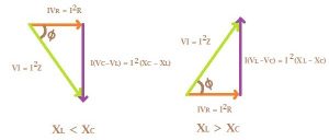
Mutual Inductance Coupling Coefficient

The mutual inductance coupling coefficient is a measure of the coupling efficiency between two coils. It quantifies the extent to which the magnetic field produced by one coil links with the other coil. The coupling coefficient ranges from 0 to 1, where 0 indicates no coupling and 1 represents perfect coupling. It is an important parameter in the design and analysis of transformers and inductive coupling systems.

Mutual Inductance Derivation

The derivation of mutual inductance involves mathematical calculations based on the principles of electromagnetic induction. It takes into account factors such as the number of turns in the coils, the magnetic flux linking the coils, and the geometry of the coils. By understanding the derivation of mutual inductance, one can gain insights into the physics of inductance and its role in electrical circuits.

Mutual Inductance of Two Coils Formula

The mutual inductance between two coils can be calculated using a formula that takes into account various parameters. The formula involves the number of turns in each coil, the magnetic flux linking the coils, and the geometrical arrangement of the coils. This formula is widely used in the design and analysis of transformers, where mutual inductance plays a crucial role in transferring electrical energy from one coil to another.

By understanding these advanced concepts related to mutual inductance, one can gain a deeper insight into the physics of inductance and its applications in electrical engineering. These concepts are fundamental to the study of electromagnetic fields, reactance, impedance, resonance, and the calculation of inductance in various electrical systems.

Frequently Asked Questions

Is Mutual Inductance Always Positive?

No, mutual inductance can be positive or negative depending on the orientation of the coils and the direction of the current. Mutual inductance is a measure of the interaction between two coils and is defined as the ability of one coil to induce a voltage in the other coil. If the current in one coil produces a magnetic field that reinforces the magnetic field of the other coil, the mutual inductance is positive. Conversely, if the magnetic fields oppose each other, the mutual inductance is negative.

Does Mutual Inductance Depend on Current?

Yes, mutual inductance depends on the current flowing through the coils. According to Faraday’s law of electromagnetic induction, the induced voltage in a coil is directly proportional to the rate of change of magnetic flux through the coil. Therefore, the greater the current flowing through a coil, the stronger the magnetic field it produces, and the higher the mutual inductance between the coils.

How to Measure Mutual Inductance?

Mutual inductance can be measured using various techniques. One common method is to connect the two coils in series and apply an alternating current to one of the coils. By measuring the voltage induced in the other coil, the mutual inductance can be determined. Another method involves using a mutual inductance bridge circuit, which allows for more precise measurements. Additionally, mutual inductance can also be calculated indirectly by measuring the self-inductance of each coil and using the mutual inductance formula.

How to Calculate Mutual Inductance of a Transformer?

The mutual inductance of a transformer can be calculated using the formula:

M = (k * √(L1 * L2))

Where M is the mutual inductance, k is the coupling coefficient (a value between 0 and 1 that represents the degree of magnetic coupling between the coils), L1 is the self-inductance of one coil, and L2 is the self-inductance of the other coil. The mutual inductance is typically measured in henries (H).

Difference Between Mutual Induction and Mutual Inductance

Mutual induction and mutual inductance are related concepts but have distinct meanings. Mutual induction refers to the process by which a changing current in one coil induces a voltage in another coil. It is a fundamental principle of electromagnetic induction and is the basis for the operation of transformers and inductive coupling in electrical circuits.

On the other hand, mutual inductance is a quantitative measure of the interaction between two coils. It represents the ability of one coil to induce a voltage in the other coil and is determined by factors such as the number of turns, the orientation of the coils, and the current flowing through them. Mutual inductance is calculated using the mutual inductance formula and is expressed in henries (H).

In summary, mutual induction is the phenomenon, while mutual inductance is the measure of that phenomenon. Understanding the concepts of mutual induction and mutual inductance is essential in the study of inductors, transformers, and the physics of inductance in electrical engineering.

Conclusion

In conclusion, mutual inductance is a fundamental concept in the field of electromagnetism. It refers to the phenomenon where a changing current in one coil induces a voltage in another nearby coil. This mutual interaction between the coils is crucial in various applications, such as transformers and inductors.

Mutual inductance plays a vital role in the efficient transfer of energy between different circuits. It allows for the transformation of voltage levels, enabling the transmission of electrical power over long distances. Additionally, mutual inductance is utilized in devices like electric motors and generators, where the conversion of electrical energy to mechanical energy is required.

Understanding mutual inductance is essential for engineers and scientists working in the field of electronics and electrical engineering. It provides the foundation for designing and analyzing complex circuits and systems. By grasping the principles of mutual inductance, we can harness its power to create innovative technologies that shape our modern world.

Multiple Choice Questions

MCQ on Inductor

  1. What is an inductor?
  2. A. A device that stores electrical energy in a magnetic field
  3. B. A device that converts electrical energy into mechanical energy
  4. C. A device that generates electrical energy from light
  5. D. A device that regulates the flow of current in a circuit

  6. Which of the following is true about inductance?

  7. A. It is the property of a circuit that opposes changes in current
  8. B. It is the property of a circuit that allows easy flow of current
  9. C. It is the property of a circuit that converts electrical energy into mechanical energy
  10. D. It is the property of a circuit that regulates the voltage

  11. What is the unit of inductance?

  12. A. Ampere (A)
  13. B. Ohm (Ω)
  14. C. Henry (H)
  15. D. Volt (V)

  16. Which formula is used to calculate the inductance of a coil?

  17. A. Ohm’s Law
  18. B. Faraday’s Law
  19. C. Henry‘s Law
  20. D. Coulomb’s Law

MCQ on Mutual Inductance Transformer Related

CodeCogsEqn 55 convert.io
  1. What is mutual inductance?
  2. A. The property of a circuit that opposes changes in current
  3. B. The property of a circuit that allows easy flow of current
  4. C. The property of a circuit that converts electrical energy into mechanical energy
  5. D. The property of a circuit that relates the change in current in one coil to the change in current in another coil

  6. What is a transformer?

  7. A. A device that stores electrical energy in a magnetic field
  8. B. A device that converts electrical energy into mechanical energy
  9. C. A device that generates electrical energy from light
  10. D. A device that transfers electrical energy between two or more coils through electromagnetic induction

  11. How is mutual inductance calculated in a transformer?

  12. A. By using Faraday’s Law
  13. B. By using Ohm’s Law
  14. C. By using Henry’s Law
  15. D. By using Coulomb’s Law

  16. What is inductive coupling?

  17. A. The transfer of energy between two coils through mutual inductance
  18. B. The transfer of energy between two coils through self-inductance
  19. C. The transfer of energy between two coils through capacitive coupling
  20. D. The transfer of energy between two coils through resistive coupling

Remember to choose the most appropriate answer for each question. Good luck!

Detailed Solutions to Problems and MCQs

Welcome to the detailed solutions section, where we will explore various problems and multiple-choice questions related to electromagnetic induction, Faraday’s law, and other concepts in the field of inductance. Let’s dive right in!

[]

In this section, we will focus on the concept of electromagnetic induction and its applications. Electromagnetic induction is the process of generating an electromotive force (emf) in a conductor when it is exposed to a changing magnetic field. This phenomenon, discovered by Michael Faraday, forms the basis of many electrical devices and plays a crucial role in electrical engineering.

To understand the principles of electromagnetic induction, let’s start with a simple example. Imagine we have a coil of wire and a magnet. When we move the magnet towards the coil, the magnetic field passing through the coil changes. This change in magnetic field induces an emf in the coil, causing an electric current to flow. This is the basic principle behind generators and electric motors.

Now, let’s move on to some problems and multiple-choice questions to test our understanding of electromagnetic induction and related concepts. Here are a few examples:

  1. Problem: Calculate the magnetic field strength inside a solenoid with 500 turns and a current of 2A flowing through it.
    Solution: We can use the formula for the magnetic field inside a solenoid, which is given by B = μ₀ * n * I, where B is the magnetic field strength, μ₀ is the permeability of free space, n is the number of turns per unit length, and I is the current. Plugging in the values, we get B = (4π * 10^-7 T*m/A) * (500 turns/m) * (2A) = 0.004 T.

  2. Multiple-Choice Question: Which of the following is an example of inductive coupling?
    a) Capacitor
    b) Transformer
    c) Resistor
    d
    ) Diode
    Answer
    : b) Transformer

  3. Problem: Calculate the self-inductance of a coil with an inductance of 5 H and a current changing at a rate of 2 A/s.
    Solution
    : We can use Faraday’s law of electromagnetic induction, which states that the emf induced in a coil is equal to the rate of change of magnetic flux through the coil. The formula for self-inductance is L = Φ/I, where L is the self-inductance, Φ is the magnetic flux, and I is the current. Rearranging the formula, we get Φ = L * I. Plugging in the values, we get Φ = (5 H) * (2 A/s) = 10 Wb.

These are just a few examples to give you an idea of the types of problems and multiple-choice questions you may encounter when studying electromagnetic induction and inductance. Remember to practice and understand the underlying concepts to excel in this field.

In conclusion, electromagnetic induction and the concepts of inductance play a crucial role in electrical circuits and the field of electrical engineering. Understanding the principles behind electromagnetic induction, Faraday’s law, and other related concepts is essential for designing and analyzing electrical systems. So keep exploring and learning more about the fascinating world of inductance and its applications!

Frequently Asked Questions

1. Can mutual inductance be negative?

No, mutual inductance cannot be negative. It is a measure of the amount of magnetic flux generated in one coil due to the change in current in another coil. It is always a positive value, as it is based on the absolute value of the magnetic field interaction between the two coils.

2. What is the mutual inductance formula?

ckmi2

The mutual inductance formula is M = N2Φ/I1, where M is the mutual inductance, N2 is the number of turns in the second coil, Φ is the magnetic flux through one loop of the second coil, and I1 is the current in the first coil.

3. What does mutual inductance mean?

Mutual inductance is a property that exists between two coils when the change in current in one coil induces a voltage in the other coil. It is a fundamental concept in electromagnetic induction and is measured in Henrys (H).

4. How to measure mutual inductance with an LCR meter?

To measure mutual inductance with an LCR meter, connect the two coils in series and measure the total inductance. Then, reverse the connections of one coil and measure the inductance again. The difference between these two measurements divided by 4 gives the mutual inductance.

5. How does mutual induction occur?

Mutual induction occurs when a change in current in one coil induces a voltage in a nearby coil. This happens due to the magnetic field produced by the current-carrying coil, which links with the turns of the nearby coil and induces a voltage in it according to Faraday’s law of electromagnetic induction.

6. What is the mutual inductance of a pair of coils?

ckmi

The mutual inductance of a pair of coils is a measure of how much a change in current in one coil will induce a voltage in the other coil. It depends on factors like the number of turns in each coil, the area of the coils, the distance between the coils, and the medium in which the coils are located.

7. How to reduce mutual inductance?

Mutual inductance can be reduced by increasing the distance between the coils, decreasing the number of turns in the coils, or orienting the coils so that their magnetic fields do not interact significantly.

8. What is the mutual inductance in a transformer?

In a transformer, the mutual inductance is the property that allows the transfer of energy from the primary coil to the secondary coil. It is a measure of how effectively the magnetic field generated by the primary coil induces a voltage in the secondary coil.

9. What is the symbol for mutual inductance?

The symbol for mutual inductance is ‘M’. It is measured in Henrys (H).

10. How is the mutual inductance of a pair of coils affected when the distance between them changes?

The mutual inductance of a pair of coils decreases as the distance between them increases. This is because the magnetic field generated by one coil has less effect on the other coil when they are further apart.

13 Vital Facts on D Flip Flop: Circuit, Truth Table, Working

d flip flop

A D Flip Flop stores a single bit of data; its output mirrors the input (D) when the clock (CLK) is high. Truth table: When CLK=1, if D=0, output Q=0, if D=1, Q=1; When CLK=0, Q remains unchanged. It’s edge-triggered, changing state only at clock edges, ensuring stable data storage and synchronization in digital circuits. Ideal for shift registers, data storage, and synchronizing asynchronous inputs.

A flip flop is the fundamental sequential circuit element, which has two stable states and can store one bit at a time. It can be designed using a combinational circuit with feedback and a clock. D Flip-Flop is one of that Flip Flop that can store data. It can be used to store data statically or dynamically depends on the design of the circuit. D Flip-Flop is used in many sequential circuits as register, counter, etc.

What is D flip flop ?

D flip-flop or Data flip flop is a type of flip Flop that has only one data input that is ‘D’ and one clock pulse input with two outputs Q and Q bar. This Flip Flop is also called a delay flip flop because when the input data is provided into the d flip-flop, the output follows the input data delay by one clock pulse.

d type flip flop

Full Form of D flip flop

D stands for Delay or Data in D flip-Flop.

D flip flop Diagram

The given circuit represents the D flip-flop circuit diagram, where the whole circuit is designed with the help of the NAND gate. Here the output of one NAND gate is feed as one input to the other NAND gate, which forms a latch. Then, the latch is gated with two more NAND gates where D is one input and clock is the other input. 

d flip flop
Fig. Circuit diagram of the D flip-flop designed with NAND gate

The final output of the D flip-flop is Q and Qbar, where Qbar is always complementary to Q.

D Flip Flop Truth Table

What is D Flip Flop Truth Table ?

The truth table of the d flip flop shows every possible output of the d flip-flop with the all possible combination of the input to the d flip flop, where Clock and D is the input to the D flip-flop and Q and Qbar is the output of the D flip-flop.

CLOCKDQQbar
00NO CHANGENO CHANGE
01NO CHANGENO CHANGE
1001
1110

D flip flop Excitation Table

The exaltation table or state table shows the minimum input with respect to the output that can define the circuit. Which mainly represents a sequential circuit with its present and next state of output with the preset input and clock pulse. This table is also known as a characteristic table for D flip-flop.

DinCLKPresent state ‘Q’Next state ‘Q’
X000
X011
0100
0110
1101
1111

D flip flop Boolean Expression

The boolean expression of the D flip-flop is Q(t+1)=D because the next value of Q is only dependent on the value of D, whereas there is a delay of one clock pulse from input D to output Q.

d flip flop
Fig. K- map of input (D) and output (Q) of the D flip-flop

How D Flip Flop Works ?

Working of D flip flop

D Flipflop is a bi-stable memory element, which can store one bit at a time, either ‘1’ or ‘0’. When the D input is provided to the Flip Flop, the circuit check for the clock signal is the signal of the clock is high ( for level triggered d flip-flop) then with every clock pulse, the input D propagates to the output Q. 

For edge triggered flip-flop, the circuit check for the transition of clock pulse according to which the flip Flop propagates the input to the output; edge triggered can be positive edge triggered or negative triggered. Positive edge triggered D flip-flop changes its output according to input with every transition of the clock pulse from 0 to 1. As for the negative edge triggered D flip-flop changes its output according to input with every transition of the clock pulse from 1 to 0.

D flip flop Timing Diagram

As shown in the given figure, there is a clock pulse representation, with which D, which is the input to D flip-flop, and Q which is the output, is represented, where Qbar is the complement output of the output Q, here we see the timing diagram of a positive edge flip flop, that’s why here the output changes with every positive transition in the clock pulse according to the input.

image 13
Fig. Timing or Waveform diagram of the D flip-flop (positive edge triggered).

D flip flop Block Diagram

The diagram shown below is the block representation of the d flip-flop, where D is the input, the clock is another input to the Flip Flop, where a preset and clear signal is used to set or reset the output Q of the D flip-flop. 

What is D flip flop Symbol ?

image 14
Fig. Block representation of the D flip-flop with preset and clear

D flip flop Clear and Preset

The given figure is the block diagram of a D flip-flop having preset/set and rest / clear as additional input to the Flip Flop, where Preset/Set is used to set the output Q of the flip Flop set to 1. Rest/Clear is to set the output Q of the flip Flop to 0.

image 15
Fig. Block diagram of the D flip-flop with preset/set and reset/clear

D flip flop with Set

D flip-flop can have set the input as a requirement, and it can change the output and set the output Q to 1. It can be synchronous or asynchronous, Synchronous when the output can change only with the clock pulse, asynchronous is when the output can be set to 1 at any point of time regardless of the clock pulse.

D flip flop with Reset

D flip-flop can sometimes reset / clear input only in addition to data input and clock input, resetting the output Q to zero of the d flipflop as a requirement. Reset/Clear be active low input or active high input depends on the Flip Flop design.

Asynchronous Set and Reset

D flip flop with Asynchronous Set and Reset

D flip-flop can have an asynchronous set/preset and reset/clear as input independent of the clock. That means the output of the Flip Flop can be set to 1 with preset or reset to 0 with the reset despite the clock pulse, which means the output can change with or without a clock, which can result in asynchronous output.

D flip flop with Asynchronous Reset

D flip-flops can have asynchronous reset, which can be independent of the clock. Regardless of the clock, the reset can change the output Q to zero, which can cause asynchronous output.

D flip flop with Synchronous Reset

D flip-flop with synchronous reset means the output can reset to zero with the reset input but only with the clock, which makes the reset input dependent on the clock pulse; without clock pulse reset will not be able to set the output Q to zero, which will give you a synchronous output always.

D Flip Flop with Enable

Other than set/preset or reset/clear D flip-flop can have enabled as one input when enable is high, the Flip Flop can operate with the data input and clock input, but when the enable is low then regardless of any other input, the flip Flop stays in a hold state.

image 16
Fig. Block representation of a D flip-flop with Enable

D flip flop with Enable Truth Table

EnableDQn01NO CHANGE00NO CHANGE111100Table: D flip-flop truth table with enable input


D flip flop Truth Table with Preset and Clear

PR (ACTIVE LOW)CLR(ACTIVE LOW)CLKDQQbar
01XX10
10XX01
00XXNOT DEFINEDNOT DEFINED
111110
111001
111XNO CHANGENO CHNAGE
Table: D flip-flop table with preset, clear and clock

D flip flop Truth Table with Clock and Reset

CLKRESETDQ
0XXNO CHANGE
11X0
1011
1000
Table: D flip-flop Truth table reset and clock input

Asynchronous D flip flop

When D flip-flop generates output independent of the clock signal, then the output produced may be asynchronous. It is mainly caused by an asynchronous set/preset or clear/reset signal, which can set or reset the output of the flip Flop at any intent of time, which disrupt synchronicity in the D flip-flop.

State Diagram for D Flip Flop

The state diagram is the representation of a different stable state with the transition between the states with the cause of transition. Here every stable state output of the D flip-flop is represented with a circle. In contrast, the transition between the state is represented by the arrow between the circle, which is leveled with the cause of the transition.

image 17
Fig. State diagram of the D flip-flop

When the state changes from 0 to 1, it is caused by the input D, which is high, and when the output state is 0, and at the time D=0 that produces no change in the output, the arrow with D=0 starts with state 0 and also returns to state 0.

ASM Chart for D flip flop

An algorithmic state machine chart contains three blocks: state block, condition block, and conditional output box. The rectangle box represents one state; the diamond box is the condition box true or false if the condition decides the branch to follow.

image 18
Fig. ASM (algorithmic state machine) chart representation of the D flip-flop

D flip flop schematic | D Flip Flop Schematic Circuit | D Type Flip Flop Schematic

The figure shows the schematic representation of the D flip-flop; the schematic diagram represents the procedure using abstract. 

Two diagrams show the working of the D flip-flop when the clock is high and another showing when the clock is low. When the clock is high, the input data passes through the circuit, but when the clock is low, the input can not pass through the circuit, which shows regardless of the change in input, there will be no change in output when the clock is low.

image 19
Fig. Schematic diagram representation of the d flip-flop. one figure with clock pulse low and other with clock pulse high

Dynamic D flip flop

Flip Flop is generally a static storing device, but a dynamic flip flop can dynamically store data. In the given schematic diagram of a dynamic flip flop, we can see a capacitor connected to each stage. When there is no clock pulse for a long time, the capacitor’s charge can be lost. However, because of the presence of the capacitor, the circuit will be able to store data dynamically.

image 20
Fig. A Schematic diagram of the Dynamic D flip-flop

Dynamic D flip-flop is designed for faster operation; the area covered by dynamic flip flop is less than that of a static flip flop.

D flip flop Metastability

Metastability refers to the state where output is not deterministic. It can cause oscillation, unclear transitions in the circuitry. For example, flip Flop faces the problem of metastability; it happens to a flip flop when the clock pulse and data change at the same instate of time, which causes the result to behave unpredictably.

To avoid metastability in flip Flop the operation of flip Flop should operate considering the setup time and hold time of the Flip Flop. Still, metastability cannot be eliminated completely, but it can be minimized.

Application of D flip flop

Important applications of D flipflop listed as follows :

  • D flip-flop can be used to produce a controlled delay in the circuitry.
  • Used to design frequency divider circuity.
  • For creating counters.
  • For developing registers.
  • Used in pipelining.
  • For synchronization.
  • Can be used to avoid glitches.
  • Used to fix clock frequency as for the requirement of the circuitry.
  • Can be used for isolation.
  • As Toggle switch.
  • Can be used for Data transmission.
  • Sequence generator.
  • Can be used as a memory element.

Difference Between D and T flip flop

D FLIP-FLOPT FLIP FLOP
The output of a d flip flop follows the input with a delay of one clock pulse.The output of T flip flop toggles with a high input with every clock pulse.
It is known as delay flip flopIt is known as toggle flip flop
With low input the output also changes to low with clock pulseWith low input the output does not change at all, it stays in hold state.

Difference Between D flip flop and JK flip flop

D flip-flopJ K flip flop
The output of a d flip flop follows the input with a delay of one clock pulse.The output of a J K flip flop sets to 1 with J and resets to 0 with R  when there is clock pulse.
It is known as delay flip flop.It is also called universal flip flop.
It has less number of input combinations.It has more number of input combinations.

Difference Between D latch and D flip flop

D latchD flip-flop
D latch is a gated SR latch, which do not have clock input D flip-flop is combination of D latch with clock input
Less complex circuitComplex circuit
D latch is has enable signal which can enable or disable the latch operationD flip-flop has clock signal which can hold or operated the flip flop when no set or reset input is available.
D latch can be active high input or active low input latch.D flip-flop in which data input is always active high, where set or reset input can be active high or active low input.
D latch is always a level triggered circuit.D flip-flop can be level triggered or edge triggered circuit.
Less number of transistor is required for design.More number of transistor is required for design.
Asynchronous in nature.Generally synchronous in nature.

Q: What is a flip-flop in digital electronics?

A: In digital electronics, a flip-flop or latch is a circuit that has two stable states and can be used to store state information. They are fundamental building blocks in sequential logic, with the D-type flip flop being a commonly-used type.

Q: What is a d-type flip flop?

A: A D-type flip flop is a type of flip flop circuit that has a D (data) input and a clock input. The D flip-flop captures the value of the D-input at a definite portion of the clock cycle (such as the rising edge). This can be thought of as the flip flop “sampling” the D input and storing it.

Q: How do logic gates interact in a d-type flip flop?

A: A D-type flip flop can be implemented using a combination of logic gates such as AND and OR gates, as well as inverters. The particular arrangement of these gates determines the output of the flip-flop for each input condition.

Q: What distinguishes a d-type flip flop from an sr flip-flop?

A: One key difference is that an SR flip-flop requires two inputs, namely S (Set) and R (Reset), while a D-type flip flop takes both a data input and a clock input. Consequently, the behaviour and use cases of these flip flop types are different in digital electronics.

Q: Can you explain the working of a D flip-flop action on the rising edge of the clock?

A: The D flip-flop is sensitive to the clock edge, i.e., the transition from low to high (rising edge) or high to low (falling edge). When the clock signal goes from low to high on the rising edge, the value on the D input is transferred to the flip-flop’s output. At other times, the output remains what was last stored.

Q: How does a D flip flop compare to a JK flip-flop?

A: The JK flip-flop and the D type flip-flop are two types of flip-flops in digital electronics. The JK flip-flop, like the SR flip-flop, has two inputs but does not have the invalid state that the SR flip-flop has when both inputs are 1. The D flip-flop, on the other hand, eliminates this ambiguity by having only one input that determines what state the flip flop will change to, with the change in state being triggered by a clock edge.

Q: How does a D flip-flop function in shift registers?

A: In a shift register, multiple D flip-flops are chained together in a configuration known as a cascade. Each flip-flop passes its output as the input to the next flip-flop on each clock cycle, effectively shifting the binary data held by the register.

Q: What is a truth table in the context of a D flip-flop?

A: A truth table for a D flip-flop is a table that describes how the output of the flip-flop depends on its current output and current input. For a D-type flip-flop, the next state is exactly what the data input is at the time of a positive clock edge.

Q: What is the characteristic equation of a D flip- flop?

A: The characteristic equation of a D flip-flop is simple: The next output Q(next) equals the current input D (Q(next) = D). This is as per data input from the flip flop at the time of a positive clock edge.

Q: How does a delay flip-flop (D FF) work?

A: A delay flip-flop (D FF), sometimes known as a D-type flip-flop, behaves just like a wire delayed by one clock period. It takes an input signal and outputs that same signal, but delayed by one clock cycle. In essence, the D FF “remembers” the input value at the rising edge of the clock and delays it by one clock cycle.

Q: What is an SR flip-flop in digital electronics?

A: An SR flip-flop, one of the types of flip-flops in digital electronics, is a form of a sequential logic circuit often utilized for data storage. An SR flip-flop requires two inputs, specifically, the set (S) and reset (R) inputs. The output changes or retains its state when it faces different input conditions, making it a fundamental building block of digital electronics.

Q: How does a D-type flip flop work?

A: A D-type flip-flop operates with a data input and a clock input. At the rising edge of the clock input, the d-type flip flop transfers the input data to the output. Thus, it acts as a delay or edge-triggered device in digital electronics, transmitting the data input from the flip flop’s input to its output during clock pulses.

Q: What is a JK flip-flop?

A: A JK flip-flop is another type of flip flop circuit found in digital logic. It extends the functionality of the SR flip flop by addressing the input condition issue where both inputs are 1. With a JK flip-flop, this state triggers a toggle, causing the flip flop to change state at every clock edge.

Q: What are logic gates, and how do they relate to flip flops?

A: Logic gates are fundamental building blocks in digital electronics that process binary inputs to produce a binary output based on the type of gate. Flip flops, including D-type and SR flip-flops, are composed of interconnected logic gates. The combination of these logic gates determines how a flip flop behaves in terms of its characteristic equation.

Q: Can flip flops be used as shift registers in digital logic?

A: Yes, flip flops can be utilized to implement shift registers in digital logic. A shift register is a sequential device that utilizes flip-flops to store binary data. In a shift register, data is passed from the output of one flip flop to the inputs of the next flip-flop in a cascade configuration, in synchronization with clock pulses.

Q: What are the input signals in a flip flop?

A: The input signals in a flip flop vary depending on the type of flip flop circuit used. For an SR flip-flop, the two inputs are known as set and reset. For a D-type flip-flop, the two inputs are data and clock. An additional input, known as ‘enable’, may be used in certain types of flip-flops.

Q: What happens when a flip flop receives a rising edge input signal?

A: When a flip flop receives a rising edge input signal, i.e., a transition from a low voltage to a high voltage, a state change typically occurs. In a D-type flip flop, for instance, the state of the data input is captured at the moment of the rising edge of the clock and is transferred to the output.

Q: What role does an inverter play in the operation of a flip flop?

A: An inverter, another basic block of digital electronics, plays a crucial role in the functioning of a flip flop. It is used in a flip flop circuit to invert the output, specifically, a high output becomes low, and vice versa. In the SR flip-flop, for instance, an inverted output from one part of the circuit is often looped back as an input to another part, creating a form of feedback that enables the flip flop to maintain its state.

Q: What is meant by ‘since the output of a flip flop would always change’?

A: When we say ‘since the output of a flip flop would always change’, we’re referring to the inherent characteristic of a flip flop as a bistable device. This means that it has two stable states and can transition between these states based on its input. Thus, depending on the input conditions and type of flip flop circuit, the output of the flip flop can change or retain its prior state, making it a crucial component in digital electronics where data storage and transfer are required.

Q: What leads a flip flop to change state?

A: A flip flop changes state based on its input signal(s). For instance, an SR flip-flop changes state when either the Set or Reset input is activated, and a D-type flip flop changes state based on the data input at the moment of a clock edge, especially a rising edge. The change state feature of flip flops makes them pivotal in designing digital systems for various applications, from basic data storage units to complex microprocessors.