29 Facts On Comparator Circuit:What,How,Design,Working,Types

C1

What is comparator circuit ?

A comparator or a voltage comparator is a device used to compare two voltage levels. We can determine which voltage level is higher from the comparator’s output. It is an application of typical op-amps, and it has applications furthermore.

What does a comparator circuit do ?

A comparator compares two given input voltage and provides the output indicating which voltage has a more excellent value. The circuit takes input using inverting and non-inverting terminals and provides output from the output terminal. The output range lies between the positive saturation voltage and negative saturation voltage.

comparator circuit

Op Amp comparator circuit

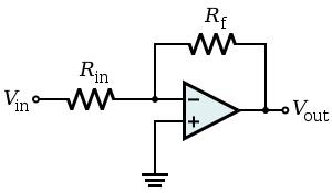
The below image represents a circuit diagram of the comparator circuit. As we can observe that the circuit comprises only an op-amp, and voltage inputs are supplied in it through the inverting and non-inverting terminals.
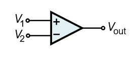
C1
Image By –InductiveloadOp-Amp Comparator, marked as public domain, more details on Wikimedia Commons

Comparator circuit design

The comparator circuit is designed using an op amp. To make it ready for operation, input voltages are provided. There is no feedback system incorporated with it. A reference voltage and a voltage signal are provided through the op-amp. The positive and negative saturation voltage inputs are also provided. The indicative output is collected from the output of the op-amp.

How comparator circuit works ?

The working principle of the comparator is pretty simple. In general, it compares between two voltage sources and provides a greater output. Below mentioned two points state the working.

  • If the voltage in the non-inverting terminal is higher than the inverting terminal voltage, the output is switched to the op-amp’s positive saturation voltage.
  • If the inverting terminal’s voltage is higher than the voltage in the non-inverting terminal, the output is switched to the op-amp’s negative saturation voltage.

Voltage comparator circuit using op amp 741

Op-amp 741 is an integrated circuit containing an op amp. A voltage comparator can be created using op amp 741. The below image represents a non-inverting voltage comparator’s circuit diagram using op amp 741.
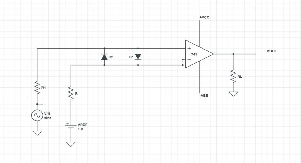
C2
Comparator using op amp 741

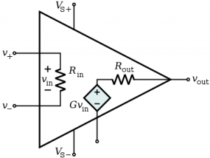
Comparator block diagram

The operation of a comparator can be represented by using block diagrams. The following image represents a block diagram of a comparator,
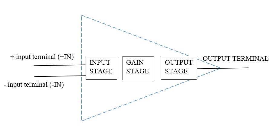
C3
Comparator Block Diagram

Comparator circuit relay

Relays are switches that can control a circuit. It can turn On or OFF a circuit and can connect and disconnect a circuit from another circuit. A comparator is broadly utilized as the utilization of the relays.

Comparator circuit uses

A comparator is a valuable and essential device. There are several applications of comparators. Some of the applications of the comparators are listed below.

  • Null Detector: If a value is zero, a null detector detects it. A comparator is typically a high-gain amplifier, and for controlled inputs, a comparator is suitable for detecting Null.
  • Level Shifter: A level shifter can be designed using a single op-amp. Using a suitable pull-up voltage, the circuit allows for a lot of versatility in selecting the voltages to be interpreted.
  • Analog-to-digital Converter (ADC): Comparators are used to create analog-to-digital converters. In a converter, the output indicates which voltage is higher. This operation is the same as a 1-bit quantization. That is why comparators are used in almost every analog-to-digital converter.
  • Other than the mentioned applications, there are many other comparators like – Relaxation Oscillator, in Absolute Value Detectors, in Zero-Crossing Detectors, in Window Detectors, etc.

Comparator fuzz circuit

Fuzz circuits can be developed using comparators. LM311 IC is such an example of comparator fuzz. We will discuss this later about LM311.

How to make a comparator ?

A comparator is a particular and straightforward electrical device to build. To build a comparator, we need an op amp and supply voltages. At first, the op-amp is provided with positive and negative saturation voltages. The output will vary in that range of voltages. Then inputs are provided in their inverting and non-inverting terminals. The reference voltage is provided in the non-inverting terminal, and the input voltage is provided in the inverting terminal. There is no feedback system associated with this circuit.

Voltage comparator circuit

A comparator circuit can detect the high-valued voltages between two voltages. Comparators, which typically compare to voltages, are known as a voltage comparator circuit.

Phase comparator circuit diagram

A phase comparator is an analog logic circuit capable of mixing and multiplying. It detects the differences in phases between two given signals by generating a voltage signal. The below image represents the phase comparator circuit diagram.

Ic comparator circuits

As mentioned earlier, a comparator compares two voltage signals and produces an indicative output. Comparators are incorporated inside an integrated circuit for better usability. The below image represents the circuits for comparator ic.

C4
A typical Comparator IC

lM358 comparator circuit

lm358 is a comparator ic consisting of two comparators inside it. It has eight pins. This ic doesn’t require any independent external power supply for functioning each comparator. The circuit diagram of the ic is given below.
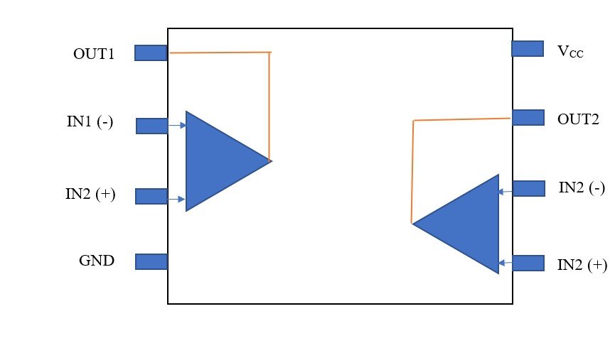
C5
LM358 Comparator IC

Comparator internal circuit

The comparator is designed using an op amp—the op amp as further circuitry. The internal circuitry inside an ic is given below in the diagram. Observing the diagram, we can see that it consists mainly of transistors, diodes, and resistors. The internal diagram can be divided into three parts based on their operation. They are – input stage, gain stage, and output stage.
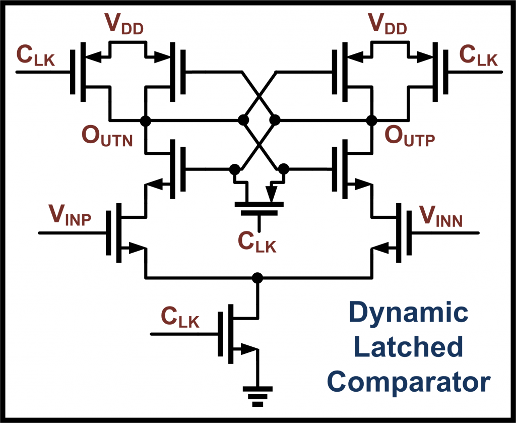
Dynamic Comparator
Comparators Internal Circuit, Image by : Guerberj at English WikipediaDynamic ComparatorCC BY-SA 3.0

Comparator circuit schematic

The schematic diagram of a comparator is given below. The internal schematic diagram is the same as an internal comparator circuit. It has diodes, transistors, and resistors. The internally connected components work as a comparator.

Schmitt trigger comparator circuit

Schmitt trigger is a viral circuit used to improve noise immunity and reduce the likelihood of multiple switching.

A schmitt trigger is a comparator circuit with separate input switching levels for changing the outputs. The schmitt trigger comparator circuit is depicted in the below diagram.

450px Op Amp Schmitt Trigger.svg
Schmitt Trigger Using two comparator – InductiveloadOp-Amp Schmitt Trigger, marked as public domain, more details on Wikimedia Commons

555 timer comparator circuit

555 timer is an oscillator circuit. It is known as 555 timers as there are three resistors of 5 kilo-ohms that are internally connected to provide the reference voltages for both the timer circuits’ comparators. A555 timer ic is used in delay timers, LED flashers, pulse generations, etc. A basic block diagram of 555 timer ic is given below. There are two comparators, an NPN transistor, a flip-flop, three 5k resistors, and an output driver.

1119px 555 esquema
Comparator Image By: Own work based on: NE555 astable.png555 esquemaCC BY-SA 3.0

comparator circuit using lm324

lm324 is a general-purpose op-amp IC that has four op-amps inside it. It can be used as a comparator also. The op-amps have properties of higher stability, wider bandwidth. LM324 has 14 pins. The pin diagram of lm324 is given below.

Pin No.Description
1First Comparator’s Output
2First Comparator’s Inverting input
3First Comparator’s Non-inverting input
45V supply voltage
5Second Comparator’s Non-inverting input
6Second Comparator’s Inverting input
7Second Comparator’s Output
8Third Comparator’s Output
9Third Comparator’s Inverting input
10Third Comparator’s non-inverting input
11Ground PIN (GND)
12Fourth Comparator’s non-inverting input
13Fourth Comparator’s Inverting input
14Fourth Comparator’s Output

The circuit diagram of the LM324 comparator is depicted in the below diagram.

lm139 comparator circuit

lm139 is another comparator ic. It has four separate precision comparators. The ic is designed to function under a single power supply. It is specially developed for directly interacting with Transistor-Transistor Logic and Complementary MOS logic. The ic comes with a propagation delay of 0.7 microseconds.

The below image depicts the internal circuit diagram of the lm139 comparator.

lm139
Comparator IC LM 139, Image by – Texas Instruments

lm319 comparator circuit

lm319 is another comparator ic having 14 pins. It has two separate precision comparators. The ic is designed to function under a wide range of supply voltages. It is specially developed for directly interacting with Transistor-Transistor Logic and Complementary MOS logic, RTL, DTL. The ic comes with a propagation delay of 0.025 microseconds.

lm311 voltage comparator circuit

lm311 is another comparator ic having eight pins. It has a single comparator. The ic comes with a response time of a minimum of 0.200 nanoseconds and a typical voltage gain of 200.

The below image depicts the internal circuit diagram of the lm311 comparator.
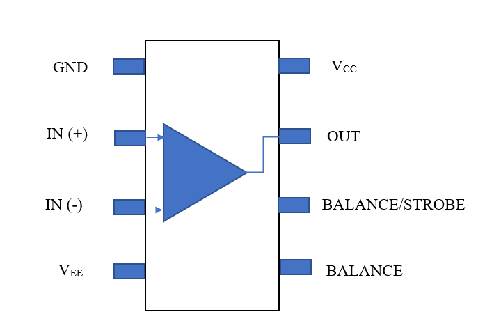
LM311
LM 311 Comparators

lm339 comparator circuit

lm339 is another comparator ic. It has four separate precision comparators. The ic is designed to function under a single power supply and for a wide range of voltages. It is specially developed for directly interacting with Transistor-Transistor Logic and Complementary MOS logic and DTL, ECL, MOS logic. The ic comes with a propagation delay of 0.7 microseconds.

Op amp comparator circuit example

Op-amp comparator circuits are used in various applications. For example – to ensure if an input value has reached the peak or the specific value or not, or for quantization in an ADC, also in window detectors, zero-crossing detectors, etc.

Voltage window comparator circuit

A window comparator refers to the circuit that works only in a particular frame or window or voltage. And a voltage comparator compares two signals and provides the output. For a window comparator circuit, there is something called the sandwich effect: if the input voltage goes higher than the low-level reference voltage. The circuit is ON, and if the input voltage gets higher than the high-level reference voltage, then the circuit is OFF.

Components required for a voltage window comparator:

  • LM741 op-amps (2)
  • 4049 Inverter Chip (1)
  • A resistor of 470 ohms (1)
  • 1N4006 Diodes (2)
  • LED

The voltage window comparator circuit is given in the below image.

<image: vol-win1>

Latching comparator circuit

A latched comparator is developed using a StrongArm latch. The StrongArm latch is considered the primary decision amplification stage. The next stage is processed out with a latching element to carry the output load.

Op amp comparator circuit with hysteresis

The difference between Upper Trip Point and Lower Trip Point is Hysteresis. Hysteresis comes with the concept of Schmitt Trigger. If a typical comparator is designed with positive feedback, that circuit causes hysteresis. The below image depicts the circuit diagram.

Regenerative comparator circuit

A Schmitt trigger circuit is also called regenerative comparator circuits. They are used to improve noise immunity and reduce the likelihood of multiple switching Regenerative comparator circuits to design other complex circuits. They are used in ADCs, slicer circuits, memory sensing, etc. The Schmitt Trigger circuit diagram is referred to as the regenerative comparator circuit’s circuit diagram.

Temperature comparator circuit

A temperature circuit is a digital electronic circuit that measures whether the input temperature is below the specified reference temperature. It is one of the primary examples of a comparator circuit. Temperature sensors include a comparator.

Frequently Asked Questions

1. How does a comparator circuit work ?

Answer: The working principle of the comparator is pretty simple. In general, it compares between two voltage sources and provides a greater output. Below mentioned two points state the working.

  • If the voltage in the non-inverting terminal is higher than the inverting terminal voltage, the output is switched to the op-amp’s positive saturation voltage.
  • If the inverting terminal’s voltage is higher than the voltage in the non-inverting terminal, the output is switched to the op-amp’s negative saturation voltage.

2. Comparator circuit types

Answer: There are several types of comparators. Some of the widely used amplifiers are listed below.

3. Why is the output voltage in the comparator circuit of an op amp equal to the saturation voltage ?

Answer: Comparator circuits do not have any feedback associated with them. The op-amp thus has an open-loop gain. For an ideal op-amp, the open-loop gain is infinite, and for a practical op-amp, the gain is very high. Now, the saturation voltage of typical op-amps is +- 15 V. The op-amp gets saturated at +13 or -13 V. Now, the op-amp gets quickly saturated for a small input voltage. That is why the output voltage in the comparator circuit equal to the saturation voltage.

4. In an op amp comparator circuit, why is a reference voltage used

Answer: Comparison is made between two or more quantities. To indicate which is more significant, we need a reference to decide. We need to determine which voltage is more significant for a comparator. That is why a reference voltage is used to make the decision.

5. How does the digital comparator circuit distinguishes between a lesser and more significant number

Answer: A digital comparator compares two binary numbers. The comparator first finds out the equivalent voltage of the binary numbers and then determines which number is less, which number is significant.

For more Electronics related article click here

23 Facts On Instrumentation Amplifier:The Complete Guide!

Instrument Amplifier

Introduction to Instrumentation Amplifier

An instrumentation amplifier is a particular type of amplifier which is derived from meeting some specific purposes. Instrumentation amplifier provides higher gain, high CMRR (common-mode rejection ratio) and high input impedances. So, we can say that it tries to possess most of the characteristics of an ideal op-amp.

An instrumentation amplifier is often called as In-Amp or InAmp. This article will discuss in detail about circuit, design, formulas, and equations related to the Instrumentation amplifier.

3 Op-Amp Instrumentation Amplifier

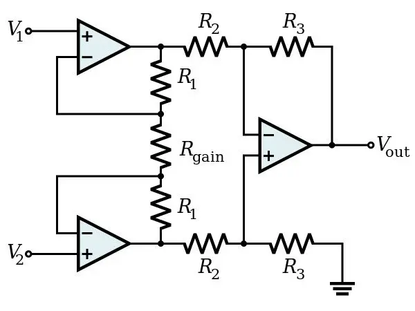
A typical Instrumentation amplifier consists of 3 regular op-amps. Two of them are used in a single-stage, whereas the other is used to separate a stage. All three amplifiers work as a differential amplifier, and all of them are connected with negative feedbacks. As instrumentation amplifiers are consisting of 3 amplifiers, they are often called three op-amp amplifier.

Instrumentation Amplifier Circuit

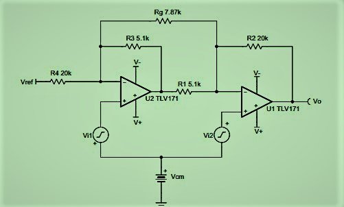
The below image represents a typical circuit diagram of an instrumentation amplifier. Carefully observe the picture as we are going to reference the photo for the rest of the article.

Instrumentation Amplifier

The input voltages are Vi1 and Vi2.

The resistances are R1 (2), R2 (2), R3, R4(2).

The voltage at A and B terminals are VA and VB, respectively.

The current through the R4, R3, and R4 branch is I.

The output of the Amplifier -1 is the Vo1, and that of amplifier -2 is Vo2.

The output of the 3rd amplifier is Vout.

Instrumentation Amplifier Design

An instrumentation amplifier is a combination of 3 typical amplifiers. They are connected in a specific order to build an instrumentation amplifier. We can segregate the instrument amplifier design into two-part.

The first part is “Two input and two output”. Two standard operational amplifiers are connected, as shown in the amplifier circuit figure. Both of them are provided with negative feedback as it stabilizes the circuit more. The output of both the amplifier is connected with three resistors.

The second part is a basic “Differential Amplifier”.  The output of both the previous amplifier acts as input for the last amplifier. Outputs are connected with two identical valued resistors with the amplifier. The positive section is grounded, and negative feedback is associated with the negative terminal and the o/p of this op-amp is the final output of the instrument amplifier.

Instrumental Amplifier Derivation

Let us derive the functional equations and formulas for the instrumentation amplifier. To derive the equations, let us know what happens inside the whole instrument amplifier. As we have previously mentioned, the separation of two stages so, we will calculate it partly.

At the first stage, the input is provided to the non-inverting terminals of both the amplifiers. The amplifier is differential amplifiers.  So, they find out the difference between the given input voltages. Now, refer to the circuit diagram; the input voltages are Vi1 and Vi2. The inverting terminal of the circuit is connected with negative feedback from the output of the amplifiers. Let us say the inverting terminals of both the amplifiers are having potentials VA and VB, respectively. They appear at the node connecting with the resistance lines and branch.

Considering the virtual short-circuit works, the A and B terminal receive the same amount of voltage as the inputs. So, we can say, VA = Vi1, VB = Vi2. The whole stage works like a differential amplifier. That means the difference between the two inputs voltage will be amplified at the output. The output will be again the differences between the two outputs voltage. That can be expressed as follow:

Vo1 – Vo2 = k (Vi1 – Vi2)

Here k is the gain of the amplifier.

At stage two, the difference of the amplifiers is fed as the input for the amplifier. The amplifier at this stage simply works like a typical amplifier. The resistances are connected with the information are of the same values as the differential amplifiers’ requirement. The inverting terminal is associated with the ground, and the amplifier is though of having virtual grounds. In the next section, we will derive the mathematical calculations for an instrument amplifier.

Instrument Amplifier Equation

The input voltages are Vi1 and Vi2.

If the virtual shorting works, then VA = Vi1 and VB = Vi2

Now, there is no current flow from A and B to the resistance branch. There is only a typical current through the branch, and that is current I. ‘I’ is given as:

I = (Vi1 – Vi2) / R3.

The current ‘I’ can also be calculated using the node analysis. It comes as follow.

I = (Vo1 – Vo2) / (R4 + R3 + R4)

Or, (Vo1 – Vo2) = (Vi1 – Vi2) * (R3 + 2R4) / R3

The above equation explains the operation of the first stage. For the second stage, the op-amp’s output is the final output of the instrumentation amplifier.

From the operation of a difference amplifier, we can write that,

Vout = (R2 / R1) x (Vo2 – Vo1)

Or, Vout = (R2 / R1) x (R3 + 2R4) x (Vi1 – Vi2) / R3

This is the instrumentation amplifier equation or the output equation of an instrumentation amplifier. Now, look at the derivation section of this article. Vo1 – Vo2 = k (Vi1 – Vi2). The obtained equation is in the same format.

Instrumentation Amplifier Gain

The amplifier’s gain is referred to as the factor by which the amplifier amplifies the input signal. The resistance values represent the gain of an instrumentation amplifier. The gain also depends on the type of feedbacks being used. The positive feedback provides higher gain, whereas negative feedback provides better stabilities of the system.

The instrumentation amplifier’s general equation is Vo1 – Vo2 = k (Vi1 – Vi2), representing the gain as: ‘k’.

Instrumentation Amplifier Gain Formula

As mentioned earlier, the amplifier gain can be derived from the output equation of the amplifier. The output equation is as follow:

Vout = (R2 / R1) x (R3 + 2R4) x (Vi1 – Vi2) / R3

Comparing this equation with the following equation:

Vo1 – Vo2 = k (Vi1 – Vi2)

We can write,

k = (R2 / R1) x (R3 + 2R4) / R3, this is the instrumentation amplifier gain formula.

Instrumentation Amplifier IC

Typical amplifiers are packaged through Integrated Circuit or ICs. So, if we want to build an Instrumental amplifier using regular op-amps, we have to use op-amp ICs. There is also a separate IC available for Instrumentation amplifiers. There is no need for connecting one op-amp with another. These types of ICs are used commercially where more numbers of ICs are used at a time.

Instrumentation Amplifier Module

Instrumentation amplifiers modules are a combination of a few electronic devices, and the main of them is the Instrumentation Amplifiers. Two of the excellent instrumentation amplifiers are AD623, AD620.

The modules are used explicitly in medical engineering devices of low powers, low power signal amplifier, thermocouples. Some of the characteristics are – a) It provides higher gain, b) Better stability, c) Low power d) High Accuracy.

Instrumental Amplifier IC List

As an instrumentation amplifier can be build using different ICs, we have made a list of all ICs that can be used for Instrumental Amplifiers. The IC numbers are given in the list.

Name of the ICIC SpecificationComments
Instrumentation AmplifierINA128Single-Chip.
Dual Instrumentation AmplifierINA212816 pin IC
Typical Op-AmpLM324IC had four amplifiers.
Instrumentation AmplifierAD623Eight pin IC having a single instrumentation amplifier
Precision Instrumentation AmplifierAD62416 pin IC  
Operational AmplifierIC741Four pin IC and works as a single unit of the op-amp.

Instrumentation Amplifier Load Cell

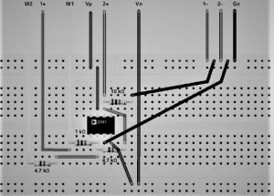
The performance of the instrumentation amplifier gradually increases upon connecting the load cell. The amplifier provides higher CMRR, higher input impedances and thus improves the performance. The detailed connection for the instrumentation amplifier with load cell is shown in the below image.

Instrumentation Amplifier offset voltage

Every op-amp has its offset voltage. The offset voltage is defined as the must need a voltage that must be applied between two inputs to nullify the difference between them and this offset value of every op-amp is specified in the datasheet provided by the manufacturer. For Instrumentation amplifiers, the offset voltage is significantly less, which is desirable.

Instrumentation Amplifier Output Waveform

To observe an instrumentation amplifier’s output, we have to connect it with a CRO (Cathode Ray Oscilloscope). We provide input as sine waves as two input signals, and work is measured from the last amplifier. Co-axial probes are connected with the pins to observe the output waveform. The below image depicts the output. The output is the amplified difference between the applied input voltages.

Instrumentation amplifier and analog multiplier waveforms Channel 1 INA output Channel
Output Waveform

Instrumentation Amplifier transfer function

The transfer function of a system refers to the process which describes or provides output for each input. As the amplifier takes two inputs and amplifies them, the transfer function will reflect the same. The transfer function can be written as:

Vo1 – Vo2 = k (Vi1 – Vi2)

Here Vi1 and Vi2 are the two inputs, and k is the gain.

Dual Instrumentation Amplifier

A dual instrumentation amplifier is a special kind of instrumentation amplifier having great accuracy. It is designed in a certain way to provide high gain, greater accuracy from a minimal size of IC. It also has a low offset voltage. For a wider bandwidth and a connected external resistor, the dual amplifier can provide gain up to 10,000.

The INA2128 IC is used as a dual instrumental amplifier. Some of the significant Applications of dual instrumentation amplifier are sensor amplifiers, medical engineering devices, and battery-operated equipment.

Instrumentation Amplifier vs Operational Amplifier

Points of ReferenceOperational AmplifierInstrumentation Amplifier
Basic StructureBuild up of Bipolar Junction Transistors or Metal Oxide Field-Effect Transistors.The buildup of three Differential Amplifiers
GainNormal GainHigher Gain
Buffer ConnectionAn operational amplifier can be used to make a buffer circuit.A buffer circuit is a part of the whole circuit.
IC specificationIC741AD623

Instrumentation Amplifier advantages and disadvantages

Instrumentation Amplifiers is developed to gain more advantages over typical differential amplifiers. That is why instrumentation amplifiers are used in most commercial applications. But it has some advantages too. Let us discuss some of the instrumentation amplifiers advantages and disadvantages.

Advantages

1. Accuracy and Precision in Measurement: Instrumentation amplifiers are used for testing and measurement purpose. Instrument amplifiers don’t need to match the input impedances. That is why they are so useful for testing. The better parametric values like higher CMRR, high input impedance also gain advantages.

2. Gain: Instrumentation amplifiers provide greater values for open-loop gain. It is a clearer advantage which is also an essential requirement for the amplifiers.

3. Stability of the System: Inside the Instrumentation Amplifiers, all normal op-amps are connected in negative feedback. As we know, negative feedback stabilises the system; the Instrumentation amplifier’s stability is also high.

4. Scalability: Instrumentation amplifiers are incredibly scalable. It provides the option to scale the signal at the input level. That is why the overall amplification is much greater than other amplifiers. The range for scaling is high for that reason also.

5. Accessibility: Instrumentation amplifiers come in ICs. There are eight-pin ICs are available. So, it is easier to handle and use. Also, there are not many factors to take during the amplification. The user just has to know the input signal well. Let us find the disadvantages of the instrumentation amplifiers.

Disadvantages

1. The Instrumentation amplifier suffers from the issue of long-range transmission. The amplifier tends to mix up the original signals with the noises if the input signal is sent for an extended range for communication. The issue can be resolved if the cable type can be improvised so that the noise gets cancelled at the primary stage or no noise enters the transmission line.

Instrumentation Amplifier Characteristics

Let us look at the characteristics of the instrumentation amplifiers at a glance.

  • Instrumentation Amplifiers are Differential Amplifiers made up of three op-amps.
  • It provides a higher open-loop gain than typical op-amps.
  • It has higher CMRR, higher input impedance, low offset voltages, lower output impedances, making it close to the ideal op-amp.
  • Instrumentation amplifiers provide higher accuracy and precision when used in testing and measuring.
  • Instrumentation amplifiers are available in ICs for commercial purposes.

2 op amp instrumentation Amplifier

Typical instrumentation amplifiers are made up of 3 amplifiers but it is also possible to make an instrumentation amplifier using a two op-amp. The below image depicts the a 2 op amp based Instrumentation Amplifier Circuit.

Annotation 2021 04 11 135148
Two op-amp Instrumentation Amplifier Circuit

instrumentation amplifier noise analysis

There are particular types of instrumentation-amplifiers available for measuring the weakest signal in a noisy environment. They are known as noise instrumentation-amplifiers. These types of instrumentation amplifiers are used for noise analysis.

Instrumentation amplifier for current sensing

Separate current sensing amplifiers are available in the market for current sensing. But an instrumentation amplifier can also operate current sensing. The primary difference between the two amplifiers is in the input topology.

Frequently Asked Questions

1. Why use an instrumentation amplifier?

Answer: Instrumentation-amplifiers provide higher gain, higher CMRR, higher input impedances, lower output impedances. Thus, we can observe it possesses very close properties of an ideal op-amp. That is why an instrumentation-amplifier is used.

2. When to use an instrumentation amplifier?

Answer: Instrumentation-amplifiers are required every time the user requires a higher gain with better stability of the system to amplify a signal. If the user needed very accurate testing results and measurements, then the instrumentation amplifier comes as a solution.

3. What is an Instrumentation amplifier for load cell?

Answer: The performance of the instrumentation-amplifier gradually increases upon connecting the load cell. The amplifier provides higher CMRR, higher input impedances and thus improves the performance. The detailed connection for the instrumentation amplifier with load cell is shown in the below image. (Point to be noted – Connect all the ground.

4. What is a circuit diagram of an instrumentation amplifier for a biosignal with a gain of a thousand?

Answer: The standard connection of the instrumentation-amplifier provides a specific gain. But adding up an external resistor will give you a boost of thousand.

5. What is the working principle of an instrumentation amplifier?

Answer: The working principle of the instrumentation amplifier is the same as that of a Differential amplifier. It takes the input voltages and amplifies the difference to provide that amplified difference as the output.

Basically: Output = Gain * (Input1 – Input2)

6. What are the advantages of using an instrumentation amplifier over an ordinary differential amplifier in measuring low signals and voltages?

Answer: The advantages are –

  • Accuracy and Precision in Measurement: Instrumentation amplifiers are used for testing and measurement purpose. Instrument amplifiers don’t need to match the input impedances. That is why they are so useful for testing. The better parametric values like higher CMRR, high input impedance also gain advantages.
  • Gain: Instrumentation amplifiers provide greater values for open-loop growth. It is a more clear advantage which is also an essential requirement for the amplifiers.
  • Stability of the System: Inside the Instrumentation Amplifiers, all normal op-amps are connected in negative feedback. As we know, negative feedback stabilises the system; the Instrumentation amplifier’s stability is also high.
  • Scalability: Instrumentation amplifiers are incredibly scalable. It provides the option to scale the signal at the input level. That is why the overall amplification is much greater than other amplifiers. The range for scaling is high for that reason also.
  • Accessibility: Instrumentation amplifiers come in ICs. There are eight-pin ICs are available. So, it is easier to handle and use. Also, there are not many factors to handle during the amplification. The user has to know the input signal well.

7. Why is CMRR important in instrumentation amplifier?

Answer: CMRR is an essential parameter for measuring the performance of an op-amp. CMRR estimates how much amount of common-mode signal will appear in the output measurement. Instruction Amplifier, being an op-amp explicitly used for measuring and testing purposes, should have the lowest CMRR. It is a basic need for the op-amp; otherwise, it will affect the measurement.

8. What is the difference between an instrumentation amplifier and an inverting adder using two op-amps?

Answer: The difference will be in workings and as well as in the parametric values. Inputs for an instrumentation amplifier is never supplied in the inverting terminals. So, there will be changes. Also, the instrumentation amplifiers have buffer circuits, and the feedbacks of them are negative feedback which increases the system’s stability. So, there are massive deviations from the actual results.

9. What is the purpose of a buffer within an instrumentation amplifier?

Answer: The buffer inside the instrumentation amplifier is helpful in many ways. The buffer increases the input impedance, which is very necessary. It also eliminates the difference between two input voltages; thus, the offset voltage value gets decreased. It also affects the CMRR.

10. What are good rules of thumb for building instrumentation amplifiers?

Answer: There is no such hard and fast rules for designing or building instrumentation amplifiers. But there are some best practices. Some of them are – a) Design the circuit symmetrically, b) Implement the gain in the first stage, c) Considers the factors of CMRR, thermocouple effects and resistance values, d) Design the second stage.

11. How to remove offset voltage in the instrumentation amplifier?

Answer: The offset voltage of any amplifier is removable by feeding an adjustable current from a voltage source. A high-valued resistor should be placed between the current and the op-amp.

For more Electronics related article click here
Op-Amp As Integrator & Differentiator : Beginner’s Guide!

differentiator

Contents

  • What is Integrator?
  • Working principle of Integrator
  • Op-amp integrator circuit
  • Output of an integrator
  • Derivation of Op-amp as integrator
  • Practical op-amp integrator
  • Applications of integrator
  • What is Differentiator ?
  • Op-amp as Differentiator
  • Working Principle of Differentiator
  • Output waveform of a differentiator
  • Applications of Differentiator

What is Integrator?

Definition of Integrator

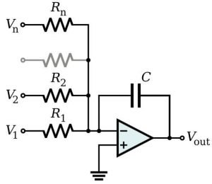
If the feedback path is made through a capacitor instead of a resistance , an RC Network has been established across the operational amplifiers’ negative feedback path. This kind of circuit configuration producing helps in implementing mathematical operation, specifically integration, and this operational amplifier circuit is known as an Operational amplifier Integrator circuit.

The output of the circuit is the integration of the applied input voltage with time.

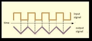
Integrator circuits are basically inverting operational amplifiers (they work in inverting op-amp configuration, with suitable capacitors and resistors), which generally produce a triangular wave output from a square wave input. Hence, they are also used for creating triangular pulses.

Op-amp as Integrator

Working principle of Integrator

Operational amplifiers can be used for mathematical applications such as Integration and Differentiation by implementing specific op-amp configurations.

When the feedback path is made through a capacitor instead of a resistance , an RC Network has been established across the operational amplifiers’ negative feedback path. This kind of circuit configuration producing helps in implementing mathematical operation, specifically integration, and this operational amplifier circuit is known as an Operational amplifier Integrator circuit. The output of the circuit is the integration of the applied input voltage with time.

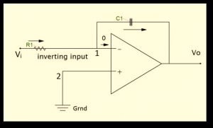
Op-amp integrator circuit

Integrator Circuit
Op-amp integrator circuit

Output of an integrator

Input Output of Integrator
input and output waveform of an integrator

Integrator circuits are basically inverting operational amplifiers (they work in inverting op-amp configuration, with suitable capacitors and resistors), which generally produce a triangular wave output from a square wave input. Hence, they are also used for creating triangular pulses.

The current in the feedback path is involved in the charging and discharging of the capacitor; therefore, the magnitude of the output signal is dependent on the amount of time a voltage is present (applied) at the input terminal of the circuit.

Derivation of Op-amp as integrator

As we know from the virtual ground concept, the voltage at point 1 is 0V. Hence, the capacitor is present between the terminals, one having zero potential and other at potential V0. When a constant voltage is applied at the input, it outcomes in a linearly increasing voltage (positive or negative as per the sign of the input signal) at the output whose rate of change is proportional to the value of the applied input voltage.

From the above circuitry it is observed, V1 = V2 = 0

The input current as:

aaa

Due to the op-amp characteristics (the input impedance of the op-amp is infinite) as the input current to the input of an op-amp is ideally zero. Therefore the current passing from the input resistor by applied input voltage Vi has flown along the feedback path into the capacitor C1.

Therefore the current from the output side can also be expressed as:

aaaa

Equating the above equations we get,

aaaaa

Therefore the op-amp output of this integrator circuit is:

b

As a consequence the circuit has a gain constant of -1/RC. The negative sign point toward an 180o phase shift.

Practical op-amp as aintegrator

If we apply a sine wave input signal to the integrator, the integrator allows low-frequency signals to pass while attenuates the high frequencies parts of the signal. Hence, it behaves like a low-pass filter rather than an integrator.

The practical integrator still has other limitations too. Unlike ideal op-amps, practical op-amps have a finite open-loop gain, finite input impedance, an input offset voltage, and an input bias current. This deviation from an ideal op-amp can affect working in several ways. For example, if Vin = 0, current passes through the capacitor due to the presence of both output offset voltage and input bias current. This causes the drifting of the output voltage over time till the op-amp saturates. If the input voltage current is zero in case of the ideal op-amp, then no drift should be present, but it is not true for the practical case.

To nullify the effect caused due to the input bias current, we have to modify the circuit such that Rom = R1||RF||RL

In this case, the error voltage will be 

bb

Therefore the same voltage drop appears at both the positive and negative terminals because of the input bias current.

For an ideal op-amp operating in the dc state, the capacitor performs as an open circuit, and hence, the gain of the circuit is infinite. To overcome this, a high resistance value resistor RF is connected in parallel with the capacitor in the feedback path. Because of this, the gain of the circuit is limited to a finite value (effectively small) and hence gets a small voltage error.

bbb
Practical Integrator
practical op-amp integrator
  • VIOS refers to the input offset voltage
  • IBI refers to the input bias current

What is Differentiator ?

Definition of Differentiator

If the input resistance in the inverting terminal is replaced by a capacitor, an RC Network has been established across the operational amplifiers’ negative feedback path. This kind of circuit configuration helps in implementing differentiation of the input voltage, and this operational amplifier circuit configuration is known as an Operational amplifier differentiator circuit.

An operational amplifier differentiator basically works as a high pass filter and, the amplitude of the output voltage produced by the differentiator is proportionate to the change of the applied input voltage.

Op-amp as a Differentiator

As we have studied earlier in the integrator circuit, op-amps can be used for implementing different mathematical applications. Here we will be studying the differential op-amp configuration in detail. The differentiator amplifier is also used for creating wave shapes and also in frequency modulators.

An operational amplifier differentiator basically works as a high pass filter and, the amplitude of the output voltage produced by the differentiator is proportionate to the change of the applied input voltage.

Working Principle of Differentiator

When the input resistance in the inverting terminal is replaced by a capacitor, an RC Network has been established across the operational amplifiers’ negative feedback path. This kind of circuit configuration helps in implementing differentiation of the input voltage, and this operational amplifier circuit configuration is known as an Operational amplifier differentiator circuit.

In a differentiating op-amp circuit, the output of the circuit is the differentiation of the input voltage applied to the op-amp with respect to time. Therefore the op-amp differentiator works in an inverting amplifier configuration, which causes the output to be 180 degrees out of phase with the input. Differentiating op-amp configuration generally responds to triangular or rectangular input waveforms.

A Differentiator Circuit

differentiators
Op-amp differentiator circuit

As shown in the figure, a connection of capacitor in series with the input voltage source has been made. The input capacitor C1 is initially uncharged and hence operate as an open-circuit. The non-inverting terminal of the amplifier is connected to the ground, whereas the inverting input terminal is through the negative feedback resistor Rf and connected to output terminal.

Due to the ideal op-amp characteristics (the input impedance of the op-amp is infinite) as the input current, I to the input of an op-amp is ideally zero. Therefore the current flowing through the capacitor (in this configuration, the input resistance is replaced by a capacitor) due to the applied input voltage Vin flows along the feedback path through the feedback resistor Rf.

As observed from the figure, point X is virtually grounded (according to the virtual ground concept) because the non-inverting input terminal is grounded (point Y is at ground potential i.e., 0V).

Consequently, Vx = Vy = 0

With respect to the input side capacitor, the current carrying through the capacitor can be written as:

cc

With respect to the output side feedback resistor, the current flowing through it can be represented as:

ccc

From the above equations when we equate the currents in both the results we get,

cccc
ccccc

The differentiating amplifier circuit requires a very small time constant for its application (differentiation), and hence it is one of its main advantages.

The product value C1Rf is known as differentiator’s time constant, and output of the differentiator is C1Rf times the differentiation of Vin signal. The -ve sign in the equation refers that the output is 180o difference in phase with reference to the input.

When we apply a constant voltage with one step change at t=0 like a step signal in the input terminal of the differentiator, the output should be ideally zero as the differentiation of constant is zero. But in practice, the output is not exactly zero because the constant input wave takes some amount of time to step from 0 volts to some Vmax volts. Therefore the output waveform appears to have a spike at time t=0.

Output Spike
Output waveform Containing spike

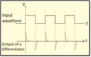
Therefore for a square wave input, we get something like shown in the below figure,

Output waveform
Output waveform of a differentiator for a square wave input

For more Electronics related article and their detail explanation  click here

.

7 Facts On Log & Antilog Amplifier:What,Working,Circuit,Use

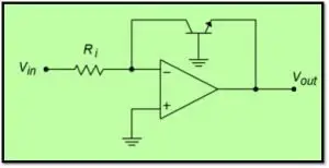
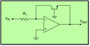
log amplifier Symbol 300x154 1

The operational amplifier circuit configurations which can perform mathematical operations such as log and antilog (exponential), including an amplification of the input signal provided to the circuit, are known as Logarithmic amplifier and Antilogarithmic amplifier respectively. In this section, we are going to learn about the Logarithmic amplifier and Antilog in detail.

Contents:

  • Introduction
  • Logarithmic (Log) Amplifier
  • Log amplifier configuration
  • Diode based Log amplifier configuration
  • Transistor based Log amplifier configuration
  • Output and Working Principle of Log Amplifier
  • Applications of the log amplifier
  • What is Antilog?
  • Antilog Amplifier
  • Log amplifier configuration
  • Diode based antilog amplifier configuration
  • Transistor based antilog amplifier configuration
  • Output and Working Principle of Log Amplifier
  • Applications of the antilog amplifier

Logarithm (Log) Amplifier

An operational amplifier in which the output voltage of the amplifier (V0) is directly proportional to the natural logarithm of the input voltage (Vi) is known as a logarithmic amplifier. Basically, the natural logarithm of the input voltage is multiplied by a constant value and produced as output.

Log Amplifier Circuit

Log Amplifier Using Transistor

Log amplifier
Log amplifier using Transistor

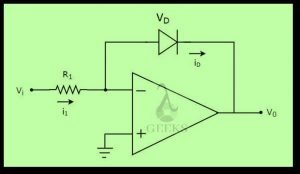
Log Amplifier using Diode

Log amplifier
Log amplifier using Diode

Output and Working Principle of Log Amplifier

This can be expressed as follows:

image002 2

Where K is the constant term, and Vref refers to a normalization constant, which we get to know in this section.

Generally, logarithm amplifiers may require more than one op-amp, in which case they are known as compensated logarithm amplifiers. They even require high performing op-amps for their proper functioning, such as LM1458, LM771, and LM714, are being some of the widely used logarithm amplifier.

The diode is connected in forward biasing. So, the diode current can be represented as:

image003 6

Where Is is the saturation current, VD is the voltage drop for the diode. The  VT is the thermal voltage. The diode current can be rewritten with high biasing condition,

image005 8

The i1 expressed by,

image007 9

Since the voltage at inverting terminal of the op-amp is at virtual ground, hence, the output voltage is given by V= -VD

Noting that i= iD, we can write

image010 3

But, as noted earlier, VD = -V0 and so,

image013 8

Taking natural logarithm on both sides of this equation, we found

image015 7

Or,  

image018 3                      

The equation of the output voltage (V0) of the logarithm amplifier contains a negative sign, which indicates that there is a phase difference of 180 o. Or, 

 image019 4                                                                       

A more advanced one utilize bipolar transistors to remove Is in the logarithmic term. In this type of logarithm amplifier configuration, the output voltage is given as:

image021 3

Applications of the logarithmic amplifier

Log amplifier is used for mathematical applications and also in different devices as per their need. Some of the applications of the log amplifier are as follows:

  • Log amplifiers are used for mathematical applications, mainly in multiplication. It is also used in the division and other exponential operations too. As it can perform multiplication operation, hence it is used in analog computers, in synthesizing audio effects, measuring instruments that require multiplication operation such as in calculating power (multiplication of current and voltage).
  • As we know that when we need to calculate the decibel equivalent of a given quantity, we require the use of a logarithmic operator, and hence, log amplifiers are used to calculate decibel (dB) value of a quantity.
  • Monolithic logarithmic amplifiers are used in certain situations, like in Radio Frequency domain, for efficient spacing (reducing components and space needed by them), and also to improve bandwidth and noise rejection.
  • It is also used in different ranges of applications such as rot mean square converter, an analog-to-digital converter, etc.

What is Antilog?

Antilog Amplifier

An Op-amp in which the output voltage of the amplifier (V0) is directly proportionate to the anti-log of the input voltage (Vi) is known as an anti-logarithmic amplifier or anti-log amplifier. Here, we are going to discuss the operational amplifier configuration that forms the anti-logarithmic amplifier in detail.

Antilog Amplifier Circuit

Antilog Amplifier Using Transistor

Antilog
Antilog Amplifier using Transistor

Antilog Amplifier using Diode

In the antilog amplifier, the input signal is at the inverting pin of the operational amplifier, which passes through a diode.

Antilog
Antilog Amplifier using Diode

Output and Working Principle of Antilog Amplifier

As observed in the circuit shown above, the negative feedback is achieved by connecting the output to the inverting input terminal. According to the concept of the virtual ground between the input terminals of an amplifier, the voltage V1 at the inverting terminal will be zero. Because of ideally infinite input impedance, the current flowing through the diode due to the applied input voltage in the inverting terminal will not enter the op-amp; instead, it will flow along the feedback path through the resistor R as shown in the figure.

The compliment or inverse function of the logarithmic amplifier is ‘exponential’,  anti-logarithmic or simply known as ‘antilog’. Consider the circuit given in the figure. The diode current is

image005 8

Where, VD is the diode voltage. According to the concept of virtual ground, V1=0 as the non-inverting terminal is grounded as shown in the figure. Therefore the voltage across the diode can be expressed as V= V– V1 or VD = Vi Hence, the current through the diode is

image025 2

Due to the ideal characteristics of an op-amp (infinite input impedance), the current flowing through the diode ( iD) flows along the feedback path through the resistor R, as we can observe in the figure.

Therefore i= i2

And, V0 = -i2R = -iDR

Replacing iD in the above equation we get 

image027 3

The parameters n, VT and Iare constants (they are only depend on the diode characteristics which are always constant for a particular diode). Therefore if the value of the feedback resistor R is fixed, then the output voltage V0 is directly proportional to the natural anti-logarithm (exponential) of the applied input voltage Vi. The above equation then can be simply represented as

 image031 3

Where K = – ISR and a = image033 1

Therefore we can notice that the anti-logarithmic op-amp produces its output signal as the exponential value of the input voltage signal applied.

The gain of the anti-log amplifier is given by the value of K that is equal to -ISR.

The –ve sign point out that there is a phase difference of 180degrees between the applied input s and the output of the anti-log amplifier.

For more Electronics related article click here

43 TestNg Interview Questions :Most Beginner’s Don’t Know

TestNg ReTry 1024x747 1 300x219 1

In this tutorial we are going to discuss the exhaustive sets of Critical TestNg interview questions and answers and distributed depending on the difficulty level, where you can better equip yourself quickly on TestNg

These Sets of Testng interview questions are distributed in the following modules or set :

TestNg Interview Questions – Advance

TestNg Interview Questions – Intermediate

TestNg Interview Questions – Basic

Testng Interview Questions and Answers || Set 1

How do you exclude a group from the test execution cycle?

You can use exclude tag to exclude a group of test case from executing in the below manner in Testng xml file 

<groups>

    <run>

        <exclude name = “excludeDummy”>

        </exclude>

    </run>

</groups>

What are the types of reports generated in TestNG by default?

TestNG generates 4 kinds of reports after the execution, which are :

  • TestNG HTML report
  • TestNG Email-able report
  • TestNG Report XML
  • TestNg Failed XML report

Mention the difference between the TestNG test suite and the TestNG test?

TestNG test suite is the collection of test classes and test methods that can be run simultaneously as well as parallelly from the TestNG XML file. 

On the other hand, the TestNG test method is a single test case file or test method.

What is the use of threadPoolSize attribute with the @Test annotation 

Through The threadPoolSize attribute we can define a thread pool with the specific mentioned size by the number for the testmethod to be executed via multiple available threads.

The attribute is being ignored if the invocationCount is not being mentioned.

@Test(threadPoolSize = 3)
public void testCaseOne(){
System.out.println("testCaseOne in process");
}

In the above test method,testCaseOne will be invoked from the three different threads.

What does alwaysRun attributes do?

This alwaysRun annotation attribute is used whenever you want to execute the test method irrespective of the dependent parameters on which the test method depends, fails. If you set to true then you need to set the attribute is true.

What are the different listeners that are available?

  • ITestListener
  • IReporter 
  • ISuiteListener
  • IAnnotationTransformer 
  • IAnnotationTransformer2
  • IHookable 
  • IInvokedMethodListener 
  • IMethodInterceptor 

What is default value for the TestNG Priority?

The TestNG priority has the default value is zero.

How to re-run TestNg Failed Tests using Auto Retry mechanism ?

TestNg provides one interface called as IRetryAnalyzer listener which you can implement the interface auto re-run your Failed Test scripts by mentioning the class in the testNg.XML file , Here is the below code for implementing the same :

TestNg ReTry 1024x747 1
Testng interview questions and answers- TestNg Retry Test Script

In the above area you can configure the number of re-try ,maximum counts and also you can mention in which all exceptions you want to re-run Test scripts.

public class Retry implements IRetryAnalyzer {
    int retryCounter = 0;
    
    // The maximum number of failed execution 
    int autoRetryLimit = 2;
    @Override
    public boolean retry(ITestResult iTestResult) {
        if (retryCounter &lt; autoRetryLimit) {
            retryCounter++;
            return true;
        }
        return false;
    }
}

Approach Two : How to re-run TestNg Failed Tests using Auto Retry mechanism

In the below approach you can build 2 classes ie one is Retry class where you can keep the logic of controlling the number of iteration in case of test failures which will implement the interface Testng IRetryAnalyzer.

Another class is basically which will implement the another interface listener IAnnotationTransformer and implement the method transform which internally interacts with the previous class (ie Retry class)

public class Retry implements IRetryAnalyzer {
    int retryCounter = 0;
    
    // The maximum number of failed execution 
    int autoRetryLimit = 2;
    @Override
    public boolean retry(ITestResult iTestResult) {
        if (retryCounter &lt; autoRetryLimit) {
            retryCounter++;
            return true;
        }
        return false;
    }
}

and finally add the CognitiveRetry class in the listener for testng.xml file .

<listeners>
    <listener class-name= "com.lambdageeks.cognitiveRetryUtils.CognitiveRetry"/>
</listeners>

How to achieve TestNG itestlistener implementation?

ITestListener is an interface in TestNg which has multiple methods(unimplemented since its an interface) which can be implemented by a class . Each method represents specific functionalities or scenarios , hence depending on your need you can implement those methods .

For an example onTestFailure is a method which you can implement where you want to perform any operations while any test method gets failed , lets say you want to capture the screenshot while in case of any test method failures , so you can write the takescreenshot method inside the onTestFailure , and as the ITestListener is an interface hence testNg will keep on listening on the events (test failures) and whenever there is test failures your screenshot will get captured .

Here is the implementation of capturing screenshot whenever you test script encounters a failures :

import org.apache.commons.io.FileUtils;
import org.openqa.selenium.OutputType;
import org.openqa.selenium.TakesScreenshot;
import org.openqa.selenium.WebDriver;
import org.testng.ITestContext;
import org.testng.ITestListener;
import org.testng.ITestResult;
import java.io.File;
import java.io.IOException;
import java.util.logging.Logger;
public class CustomListerners implements ITestListener {
    WebDriver driver=null;
    String filePath = "D:\\\\LambdaGeeks\\\\SCREENSHOTS";
    @Override
    public void onTestFailure(ITestResult result) {
        String testMethodName=String.valueOf(result.getName()).trim();
        ITestContext testContext = result.getTestContext();
        WebDriver driver = (WebDriver)testContext.getAttribute("driver");
        captureTheScreenShot(testMethodName, driver);
    }
    public void captureTheScreenShot(String methodName, WebDriver driver) {
        File scrFile = ((TakesScreenshot)driver).getScreenshotAs(OutputType.FILE);
        /*
        Each screenshots will get saved with along with the test Name to have better correlation
         */
        try {
            FileUtils.copyFile(scrFile, new File(filePath+methodName+".jpg"));
        } catch (IOException e) {
            e.printStackTrace();
        }
    }
    public void onFinish(ITestContext context) {}
    public void onTestStart(ITestResult result) {   }
    public void onTestSuccess(ITestResult result) {   }
    public void onTestSkipped(ITestResult result) {   }
    public void onTestFailedButWithinSuccessPercentage(ITestResult result) {   }
    public void onStart(ITestContext context) {   }
}

And also you need to add this class in listener tag in testng.xml file like we had done in previous question.

How to Implement testng iAnnotationtransformer ?

TestNg provides an interface named as IAnnotationTransformer that provides a method called  “transform” which you can implement and would be triggered in runtime by TestNG , this implementation is used to modify the test annotation behavior of the test class and test methods

In the below segment we would see how we could do that

public class TestClassAnnotations {
    @Test(alwaysRun = true,dependsOnMethods = "testMethodB")
    public void testMethodA() {
        System.out.println("--- Customizing the runtime behavious with ITestAnnotation ---");
    }
    @Test
    public void testMethodB() {
        System.out.println("--- Second TestMethods ---");
        Assert.fail();
    }
}

By default if we run the above code then only one method will get executed which is testMethodA and another method testMethodB will fail because we are intentionally failing this by usinig the Assert.fail() method.

But if we change the Alwaysrun=true annotation to false by using the IAnnotationTransformer then this method will not get executed , below is the code snippet on how to implement the IAnnotationTransformer and use it in the testing.xml to change the behavious of the TestNG annotation

The implementation of the CustomAnnotationTransformers goes here :

public class CustomAnnotationTransformers implements IAnnotationTransformer {
    public boolean isTestRunning(ITestAnnotation iTestAnnotation) {
        if (iTestAnnotation.getAlwaysRun()) {
            return true;
        }
        return false;
    }
    public void transform(ITestAnnotation annotations, Class testClasses, Constructor testConstructors, Method testMethods) {
        if (isTestRunning(annotations)) {
            annotations.setEnabled(false);
        }
    }
}

Here is the listener we need to add in testing.xml file

<listeners>
    <listener class-name= "com.lambdageeks.CustomAnnotationTransformers"/>
</listeners>

How to implement testng iinvokedmethodlistener?

If you want to implement a feature where a some certain method will gets executed before and after each and every Test method of TestNg then that feature could be implemented by the testng IInvokedMethodListener listener.


Here is the code snippet to implement the features :

package com.lambdageeks;
import org.testng.IInvokedMethod;
import org.testng.IInvokedMethodListener;
import org.testng.ITestResult;
public class CustomAnnotationTransformers implements IInvokedMethodListener {
    public void beforeInvocation(IInvokedMethod method, ITestResult testResult) {
        System.out.println(" ::: Before Method from IInvokedMethodListener is Triggered for the Test Method named as :  " + method.getTestMethod().getMethodName() + " ::: ");
    }
    public void afterInvocation(IInvokedMethod method, ITestResult testResult) {
        System.out.println(" :::: After Method from IInvokedMethodListener is Triggered for the Test Method named as :  " + method.getTestMethod().getMethodName() + " ::: ");
    }
}

Here is the Test Class for testing the feature :

public class TestClassAnnotations {
    @Test(alwaysRun = true)
    public void testMethoddummy() {
        System.out.println("--- This is a test Method , testing the feature of IInvokedMethodListener Testng Listener  ---");
    }
}

You have to Mention the TestNG iinvokedmethodlistener in the listener tag in the testng.xml like always

<listeners>
    <listener class-name="com.lambdageeks.CustomAnnotationTransformers"/>
</listeners>

The output of the execution would look like this :

::: Before Method from IInvokedMethodListener is Triggered for the Test Method named as :  testMethoddummy :::

— This is a test Method , testing the feature of IInvokedMethodListener Testng Listener  —

 :::: After Method from IInvokedMethodListener is Triggered for the Test Method named as :  testMethoddummy :::

How to implement Data providers in TestNG?

We can implement the DataProvider using TestNg in the below approach :

public class DataProviderDemo {
    @DataProvider(name = "dpName")
    public Object[][] dataProvidersMethodName() {
        return new Object[][]{{"Lambda"}, {"Geeks"}};
    }
    @Test(dataProvider = "dpName")
    public void dataproviderDummyTestMethod(String dataValues) {
        System.out.println("The Data Params with data provider examples : : " + dataValues);
    }
}

If we don’t set the priority of the test method in which order the tests are executed in TestNG?

The tests are executed in the order of Alphabatical order of the TestmethodName..


Such as in the below code snippet :

public class SequenceTest {
    @Test()
    public void geeks() {
        System.out.println("Sequence Test , Method ran :geeks ");
    }
    @Test()
    public void lambda() {
        System.out.println("Sequence Test , Method ran : lambda ");
    }
    @Test()
    public void abc() {
        System.out.println("Sequence Test , Method ran :abc");
    }
}

The output would look like this :

Sequence Test , Method ran :abc

Sequence Test , Method ran :geeks

Sequence Test , Method ran : lambda


How to run your Test scripts in parallel ?

You can run your Test scripts using TestNg XML file by mentioning the parallel=”methods” thread-count=”2″, here 2 parallel cases will get executed , if you want to executed more threads in parallel.

<suite name="DummyTest" parallel="methods" thread-count="2" >

<listeners>
<listener class-name="org.uncommons.reportng.HTMLReporter" />
<listener class-name="org.uncommons.reportng.JUnitXMLReporter" />
</listeners>
</suite>  

How to integrate TestNg with GRADLE build Tool?

You can run Testng Suite in gradle in different ways:

How to run TestNg Groups using Gradle : You can create a Task in build.gradle file can mention the useTestNG() and mention the below details while running the Test Groups.

TestNg Gradle
TestNg Interview Questions and Answers-TestNg with Gradle

How to run Testng Default listener with Gradle to generate report using TestNg library

TestNg Default listeners
TestNg Interview Questions and Answers- Testng With Gradle Default Listeners

If you want to use the custom listener then you can mention that same in the following approach :

Testng Gradle Custom listener 1024x497 1
TestNg Interview Questions and Answers-TestNG Custom Listeners with Gradle

How to run Testng Runner xml file using command prompt ?

You can use TestNg Downloaded location and mention org.testng.TestNg.testNgRunner.xml to run the runner xml file from the command prompt.

java -cp "/opt/testng-7.1.jar:bin" org.testng.TestNG testngRunner.xml

How to Integrate TestNg XML with Maven ?

You can integrate TestNg with Maven with the use of Plugin called maven-surefire-plugin where you can configure to run the testNgrunner.xml file using the configurations :

TestNG Maven Integration 1024x667 1
TestNg Interview Questions and Answers-TestNg-Maven-Surefire Integration

How can you specify the TestNg Test parameter using TestNg and Maven ?

You can specify the Test parameter using Maven SureFire Plugin with TestNg.XML file in the below fashion

TestNg Maven TestParameter 1024x543 1
TestNg Interview Questions and Answers-Test Parameter

Testng Interview Questions and Answers || Set 2

What is meant by invocationCount in TestNG?

invocationCount is a test annotation attribute by which you can define the number of iteration the test method will be executed in a single execution. 

 The above test will execute two times as invocationCount is mentioned as 2.

@Test(invocationCount = 2)
public void testOfInvCount() {
   System.out.println("Invocation count test in progress");
}

What are listeners in TestNG?

in TestNg the listeners are basically interface in Java which you need to implement in your class. The implemented class will keep on listening to certain events and executes the specific block of code associated with that event.Here when you implement the interface you ultimately implement the unimplemented methods and those block of code or the methods will get executed as and when specific event gets triggered. 

With the help of TestNG listeners, we can perform a lot of run time actions by listening to a different event triggered by the test script execution and their status, or we can do reporting. Also, we can change the implementation of TestNg annotation.

Mention the differences between @Factory and @Dataprovider annotations in TestNg?

@Dataprovider: When you want to execute the same test, but with different diverse sets of data in every run, you can use the dataprovider annotation, and this you can achieve the datadriven testing approach. Here the test method execution happens using the same class instance to which the test method belongs.

@Factory: This will be executed all the test methods present inside a test class using separate and multiple instances of the class.

How to use TestNG Reporter Class for the log generation?

You can log the details and data using the Reporter class, and these logs will be captured by the report generated by TestNG

Reporter.log(” Logging message “);

How to do exception handling in TestNG?

You can mention the type of expected exception in an attribute called expectedExceptions with the @test annotation; in this case, then TestNg would mark the test as passed.

@Test(expectedExceptions = numberFormatException.class)

How to achieve dependency injection via TestNg XML ?

TestNG allows us to inject dependencies between different groups of tests via the TestNG XML file. Through which we can have the dependence of one group onto another.

What are the various assertion approaches for TestNG ?

We can use two types of assertions with TestNg. 

Soft Asserts

Hard Asserts 

Mention some of the commonly used assertions with TestNG 

Some of the widely used assertion methods in TestNG :

  • assertEquals(boolean actual,boolean expected)
  • assertEqual(String actual,String expected)
  • assertEqual(String actual Result,String expected Result , String message)
  • assertTrue(condition)
  • assertFalse(condition)
  • assertFalse(condition, message)
  • assertTrue(condition, message)

What do you understand by the asserts in TestNG?

An assertion is performed to validate the actual test results with respect to the expected test results. In TestNg, we can use hard assert of soft assert. 

Difference between Hard assert and soft assert in TestNg

While working with the Hard assert, If in case we get any failure in the assertion condition then the subsequent test steps will not be executed and would be aborted, and eventually the test will be marked as a failed test case. 

While on the other hand the Soft Assert takes into considering of validating all the assertion points even if there are any failures in any of the assertions . That means the test execution does not get aborted even if one assertion fails.

How to write soft assertion in TestNg 

The below piece of code gives the approach of writing the soft assertion in TestNG

@Test
   public void assertion() {
   SoftAssert softAssertion = new SoftAssert();
   //Assertion 1 
   softAssertion.assertEquals("exp", "act");
   //Assertion 2 
   softAssertion.assertEquals(123, 123);
   //Assertion 3 
   softAssertion.assertEquals("actual Value", "expected value");
   // At the end considering all the assertion values
   softAssertion.assertAll();
}

How to use regular expression in TestNG groups?

A regular expression can be used in TestNG to execute the groups which have a similar pattern in their naming. 

For example, if you want to run all the groups starting with “testX” as per the name is concerned, then you can use the regular expression as testX.* in the TestNG XML file.

Testng Interview Questions and Answers || Set 3

What is TestNG?

TestNg basically represents “Testing Next Generation” is a unit testing framework that controls the flow and order of test automation and automation scripts by providing various annotations with their functionalities.

What are the advantages of TestNg?

  •             Through Testng’s various annotations, you can control the flow and order of automation and Test execution in a better approach.
  •             Test Classes or Test script Methods parallel execution can be achieved with TestNg.
  •            TestNg can be easily integrated with different build tools such as Maven, Gradle. Also, it can be integrated with CICD tools such as Jenkins.
  •            TestNG provide details HTML reporting feature and easily integrated with other Test reporting platform such as Allure, Extent Report with features of TestNG Listeners.
  •           All the tests can be triggered by the testng.xml file where you can mention the Test class/Test/Test Package name to be run.
  •           Data driven Testing can be done with the TestNg DataProvider annotation. Also, parameterization Tests can be done through Testng.xml as well, such as while performing cross browser testing, you can parameterize the different browsers for different tests. This feature helps to build the Data Driven Framework with TestNG.
  •          TestNg Provides a way to include/exclude a set of a test from tesngNg.xml with include and exclude attribute.
  •          With TestNg, you can group your tests and dependency injection in between the tests.
  •          TestNg provides many listeners with those you can achieve a lot of things like you can do custom reporting(IReporter), integration with different tools(ITestListener), Change the behavior of TestNG Test annotation in runtime with IAnnotationTransformer and many more.
  •         You can skip the specific test, prioritize your test order, create a time-bound test with TestNg Test annotations.
  •         You can use Hard Assertion as well as Soft Assertion with TestNg for writing Assert statement.
  •         TestNg generates TestNG-failed.xml after each Test execution, so you can you the same generated TestNG-failed.xml to rerun your failed test scripts.
  •        TestNg provides various Test annotation such as @BeforeMethod, @AfterMethod, @BeforeTest, @AfterTest.@BeforeSuite,@AfterSuite.
  •        You can run the expected exception Test with TestNg.
  •        You can rerun the failed test with IretryAnalyzer of Testng 

How do you trigger and execute the TestNg test Script?

You can run TestNg Test script in several ways : 

  •       Right Click on Test Class and “run as” and select the option of “TestNg Test.”
  •       Create testng.xml and right on the file and run the xml file.
  •       If you integrate testNg.xml with the build tool such as Maven/Gradle, then you can run from maven or Gradle as well.
  •       If the build tool such as Maven/Gradle is integrated with CICD, then you can run from CICD, i.e., from Jenkins.

State the Testng annotations that are available ?

Majorly used Testng Test annotations are :

  • @BeforeSuite
  • @AfterSuite
  • @BeforeTest
  • @AfterTest
  • @BeforeClass
  • @AfterClass
  • @BeforeMethod
  • @AfterMethod
  • @BeforeGroups
  • @AfterGroups
  • @Test

Mention the TestNg annotations execution sequence?

From the Test execution standpoint here is the below sequence for all the available TestNg annotations :

Precondition Annotations :

  • @BeforeSuite
  • @BeforeTest
  • @BeforeClass
  • @BeforeMethod
  • Test Annotations :
  • @Test
  • PostCondition Annotations: 
  • @AfterSuite
  • @AfterTest
  • @AfterClass
  • @AfterMethod

How to disable test execution for a test script?

You can use enabled attribute is equals to false in the @Test annotation attribute like mentioned below :

@Test(enabled = false)
public void logout(){
   System.out.println("Sample Test");
}

How can you specify listeners in TestNG xml?

You can use Tesng xml file for mentioning the listeners to be used as part the test script executions, in the below approach:

<suite>

<listeners>

        <listener class-name=”org.uncommons.reportng.HTMLReporter” />

        <listener class-name=”org.uncommons.reportng.JUnitXMLReporter” />

</listeners>

What is the Timeout Test in TestNg?

In this case, the “timeout test” means, if in case the test script takes longer than the specified time period to execute, then testng will abort the test and will mark as a failed test.

@Test(timeOut = 6000) // this time in mulliseconds
public void testShouldPass() throws InterruptedException {
   Thread.sleep(2000);
}

How to achieve the Expected Exception Test with TestNG?

If a Test method throws an exception, which is the same as specified as part of the test annotation expectedExceptions attribute, then TestNg would mark the test as passed.

@Test(expectedExceptions = ArithmeticException.class)
public void TestDivision() {
   int i = 1 / 0;
}

 The above Test method will be passed as it throws the exception expected by TestNG.

What is the difference between @BeforeTest and @BeforeMethod annotation?

@BeforeTest is executed once before each of the testng <test> tag mentioned in the testng.xml file 

@BeforeMethod is executed before each and every test script method.

What is the advantage of using the testng.xml file?

With the testng.xml file, you can control the flow of execution with single test suite or multiple test suite in a single testng xml file. Some of the important features are :

  • testng.xml file allows us to exclude and include test methods and test group execution.
  • You can pass test data/parameters through testng.xml.
  • You can add dependency between test methods and also a group of test methods
  • You can prioritize the test cases.
  • Parallel test execution of test cases is achieved.
  • You can implement different testng listeners and use them by mentioning those in the testng.xml.
  • If you run your suite with testng.xml, then you will only fail the test for the next iteration by using TestNG-failed.xml is generated after every execution.
  • You can run specific groups of tests using <groups>tag of TestNG xml.

How many types of dependencies can you achieve by using TestNG?

There are two types of dependencies we can achieve with TestNG : 

A. DependsOnMethods : 

By using this dependsOnMethods attribute, you are defining which test method will be dependent on other test methods, So if the depending method is failed or not run, then the dependent test method also will not run.

@Test
public void loginUserProfile() {
   System.out.println("Login user ");
}
@Test(dependsOnMethods = "loginUserProfile")
public void logOutPage_user() {
   System.out.println("Logout page for User");
}

 Here is logOutPage_user test method that will run after the successful execution of the loginUserProfile test.

B. dependsOnGroups : 

In this type of test dependency, It allows us to put the dependency injection for the test methods with a group of test methods.

The flow of execution happens in such a way ie the testGroup first gets triggered and executed and then the dependent test method gets triggered, and once after successful completion of the group test, the dependent test method will get executed.

@Test(groups="AtestGroupName")
public void testcaseOne()
{
   System.out.println("testcaseOne in process");
}
@Test(groups="AtestGroupName")
public void testcaseTwo()
{
   System.out.println("testcaseTwo in process");
}
@Test(dependsOnGroups="AtestGroupName")
public void testcaseThree()
{
   System.out.println("testcaseThree in process");
}

Conclusion : With this we conclude the list of all critical and important TestNg interview questions and answers , to get better grip on TestNg you can go through the exhaustive documentation on TestNg.

To learn more about the exhaustive Selenium tutorial you can visit here.

33 Facts On Summing Amplifier:Inverting, Non-Inverting

Summing amplifier breadboard circuit 2 300x215 1
  1. summing operational amplifier
  2. summing amplifier definition
  3. non inverting summing amplifier
  4. inverting summing amplifier
  5. summing amplifier circuit
  6. inverting summing amplifier circuit
  7. non inverting summing amplifier circuit
  8. summing amplifier with ac and dc input
  9. summing amplifier output
  10. summing amplifier waveform
  11. summing amplifier output waveform
  12. gain of a summing amplifier
  13. determine the output voltage of the summing amplifier
  14. summing amplifier derivation
  15. inverting summing amplifier formula
  16. non inverting summing amplifier derivation
  17. summing amplifier gain formula
  18. summing amplifier ic
  19. summing amplifier schematic
  20. analog summing amplifier
  21. summing and difference amplifier theory
  22. audio summing amplifier
  23. current summing-amplifier
  24. difference between inverting and non inverting summing amplifier
  25. digital to analog converter summing-amplifier
  26. function of summing amplifier
  27. single supply summing-amplifier
  28. summing-amplifier applications
  29. summing amplifier audio mixer
  30. summing amplifier dc offset
  31. summing amplifier design
  32. summing-amplifier example
  33. summing scaling and averaging amplifier
  34. summing amplifier circuit on breadboard
  35.  FAQs

Summing operational amplifier

A summing-amplifier is one of the op-amp applications, which performs summation or addition operations. Multiple input voltages are supplied into the amplifier, and the output provides an amplified summation of the voltages. Summing-amplifiers has various applications in electronics. It also has two types – inverting summing-amplifier and non-inverting summing-amplifier. In detail, we will discuss the analysis of the summing-amplifier in the following article.

summing amplifier
summing-amplifier
Image credit : Wikipedia commons

Summing amplifier definition

A summing-amplifier can be defined as An amplifier, which takes multiple inputs at one of the input terminals and provides the weighted sum of all the inputs.

Non inverting summing amplifier using op amp

Non-inverting summing-amplifier is one of the types of summing-amplifiers. In this type of operations, the input voltages are provided in the amplifier’s non-inverting terminal. The polarity of the output remains the same as the inputs and because of this, it is termed as non-inverting summing-amplifier.

Inverting summing amplifier

Inverting summing-amplifier is another type of summing-amplifier where the input voltages are provided in the inverting terminals. The polarity of the output voltages gets changed and for that reason it is known as inverting summing-amplifier.

Summing amplifier design

A summing-amplifier is designed with the help of a basic op amp and resistances. It can be designed in two main configurations

  • inverting summing-amplifier.
  • non-inverting summing-amplifier.

 We will discuss the general designing of a summing-amplifier.

To design a circuit with an op-amp, we have to keep in mind the op-amp’s basic properties. They are – high input impedance and the concept of virtual ground. For the virtual ground, we have to make a ground connection in any input terminal (the conventional way is to connect the ground in the opposite terminal where inputs are not supplied). A feedback path is created, keeping in mind the high input gain. Generally, a negative feedback path is made for system stability. The Inputs are provided with resistances. The output is collected from the output, containing the weighted sum of input.

Summing amplifier circuit | Op amp summing amplifier circuit design

The below images represent circuit diagrams of the summing-amplifier. The first one is for inverting the summing-amplifier circuit, and the second is for the non-inverting summing-amplifier circuit.

Inverting summing amplifier circuit

300px Op Amp Inverting Amplifier.svg
Image by: InductiveloadOp-Amp Inverting Amplifier, marked as public domain, more details on Wikimedia Commons

Non inverting summing amplifier circuit

300px Op Amp Non Inverting Amplifier.svg
Image by: InductiveloadOp-Amp Non-Inverting Amplifier, marked as public domain, more details on Wikimedia Commons

Observe both the circuit diagram as you can observe the difference in applying the input voltages.

Summing amplifier with ac and dc input

A summing-amplifier can be provided with either ac voltage or dc voltage. The input voltage types generally have no in the operation of the amplifier.

Summing amplifier output

The output of a summing-amplifier provides the amplified added up input voltages provided at one of the op amp input terminals. The polarity of the output voltage depends on selecting the input terminal and if the input is provided in the non-inverting terminal, the output will not be inverted. Still, if the input is provided in the inverting terminal of the circuit, there will be a polarity change.

Summing amplifier waveform

The input and output voltages of an op-amp can be observed and measured using a CRO. The CRO pins are connected with the input pins and the ground for observing the input voltages.

Summing-amplifier output waveform

To observe the output, the positive jack of the CRO is connected to the output pin, and the Negative jack is connected to the ground pin. Then we can observe the output voltage.

Gain of a summing-amplifier

The summing-amplifier is also a typical op-amp. It also amplifies the input signal and provides the output. Now, a summing-amplifier also performs the addition operation. So, it amplifies the summed-up input voltage. The general equation (of non-inverting summing amplifier) can be written as: Vo = k (V1 + V2 + … + Vn). Here, Vo is the output equation and V1, V2 … Vn are the input voltages. ‘k’ is the gain factor.

How to determine the output voltage of the summing-amplifier?

A few steps are to be followed to determine the O/P voltage of the summing-amplifier. At first, we have to use the concept of virtual ground. Using this, we make sure that voltages at both the input terminal are equal. Then apply Kirchhoff’s Current Law to get the voltage equations from the input terminals. After that, replace the necessary terms to get the final output in input voltages and resistances. Derivations for both the inverting and non-inverting types are given below.

Summing-amplifier derivation

The derivation of the summing-amplifier refers to the output equation’s derivation. The derivation includes finding out the current equation using KCL and using the concept of virtual ground ad high input impedance wherever applicable. The derivation of inverting and non-inverting summing-amplifier is done below.

Inverting summing amplifier formula

Let us determine the output formula for an inverting summing-amplifier, having ‘n’ number of inputs. Observe the circuit diagram given above.

Using the virtual ground concept, the A node’s potential is identical to potential at the B node. Applying KCL, current will be

I1 +I2 +I3 +…+IN = IO

Or, V1 /R1 + V2/R2 + … +Vn/Rn = – Vo/Rf

Or, Vo = – [(V1*Rf/R1) + (Rf*V2/R2) + … + (Rf*Vn/Rn)

Now if R1 = R2 = … = Rn = Rf, then we can write –

Vo = – [V1 + V2 + … +Vn]

This is the inverting summing-amplifier formula.

Non inverting summing-amplifier derivation

Observe the circuit diagram of the non-inverting summing-amplifier. The feedback resistance is given as Rf. The resistances for every input voltage are assumed as R1 =R2 = R3 = R.  The resistance for inverting summing-amplifier is R1. Using, the concept of virtual ground and KCL, the output equation comes as: Vo = [1 + (Rf/R1)] * [ (V1 + V2 + V3)/3]

Summing-amplifier gain formula

The output equation of an inverting summing-amplifier is given as:

Vo = – [(V1*Rf/R1) + (Rf*V2/R2) + … + (Rf*Vn/Rn)

Assuming R1 = R2 = … = Rn,

Vo = – [(V1*Rf/R1) + (Rf*V2/R1) + … + (Rf*Vn/R1)

Or, Vo = – (Rf/R1) [ V1 + V2 + … + Vn]

Now, the General equation of an inverting amplifier is:

Vo = – k (V1 + V2 + … + Vn), Where k is the gain.

So, k = (Rf/R1)

It is the gain factor of an inverting summing-amplifier.

Summing-Amplifier IC

There is no readymade summing-amplifier available in IC packaging. They are build using the conventional op-amp ICs. Op-amps, like LM358, which has a dual op-amp implemented in it, are used to make the circuit.  

Summing amplifier schematic

The schematic diagram of the summing-amplifier is given below.

375px Op Amp Internal.svg 2
Schematic of internal Circuits

Analog summing-amplifier

The amplifier is an analog device. A summing-amplifier is also used for digital to analog conversion. That is why summing-amplifiers are called analog summing amplifiers.

Summing and difference amplifier theory

The theory behind summing and difference amplifier is just the mathematical operations of addition and subtraction. In the summing-amplifiers, input voltages are provided at one end, and the output, the sum of the voltages, is received with some amplification in the output.

Same for difference amplifier, two or more voltages are provided at the input stage, and an output, the difference between them is provided with amplifications.

Both the amplifiers are also basic op-amps. So, the theory and principles of basic op-amps are also followed.

Summing amplifier uses

A summing-amplifier is a handy device. As the name recommends, the amplifier mixes up signals as required. Some of the significant applications are-

  • Audio Mixer: Summing-amplifiers are used in audio mixing for adding up various inputs with equal gains.
  • DAC: Summing-amplifiers are also used in Digital to Analog Converters.
  • Analog Signal Processing: Summing-amplifiers are efficient instruments for signal processing.

Audio summing amplifier

Audio summing-amplifier is one of the significant applications of summing-amplifiers. Audio amplifiers mix up vocals, drums, guitars and other sounds from other instruments. It is one of the essential devices for playback recordings.

DC summing-amplifier

The Dc summing-amplifier is referred to as the summing-amplifiers fed with the input dc voltages. In general, summing-amplifiers can be fed with either ac or dc voltages for their operation.

Difference between inverting and non inverting summing amplifier

Inverting and non-inverting summing-amplifiers are nothing but two different summing-amplifiers configurations and comparison in-between as follows:

Subject of Comparison Inverting Summing-Amplifier Non-inverting Summing-Amplifier
Input Input is applied in the inverting terminal of the circuit. Input is applied to the non-inverting amplifier of the circuit.
Output The output polarity gets inverted from the input. The output polarity remains the same as the input terminal signal.
Preferences An inverting summing-amplifier is more preferred comparatively. A non-inverting summing-amplifier is used in specific applications.

Differential summing-amplifier

A summing-amplifier provides an output that includes the weighted sum of inputs. Now, suppose the output of a summing-amplifier has both the negative polarity input and positive polarity voltages. In that case, that summing amplifier will be known as a differential summing-amplifier. Such amplifiers can be designed and are readily available in the market.

Digital to analog converter summing-amplifier

A digital to analog converter converts the provided digital signal into its equivalent analog signal and to know more about digital to analog converter, Click Here.

A summing-amplifier is an essential device for making a digital to analog converter, circuit diagram of a 3-bit DAC using a summing-amplifier has been shown here.

<image:4>

The output of the circuit comes as: Vo = -R [(V2/R) +(V1/2R) + (V0 / 4R)]

After simplifying the equation, we can write –

Vo = -1/4[ 4V2 + 2V1 + V0]

The output table

V2 V1 V0 Digital Value Vout (Analog Value)
0 0 0 0 0
0 0 1 1 -0.25
0 1 0 2 -0.5
0 1 1 3 -0.75
1 0 0 4 -1.0
1 0 1 5 -1.25
1 1 0 6 -1.5
1 1 1 7 -1.75

Function of summing-amplifier

The summing-amplifier’s function is to add all the input voltages provided at either inverting or non-inverting terminal and provided the output, which contains the weighted sum of all the input.

How does a summing-amplifier work

The working of a summing-amplifier is straightforward. Inputs are given at one of the input terminals. The resistances add weight to the input voltages. The amplifier then sums up all the weighted input and produces output.

Summing-amplifier dc offset

A summing-amplifier is supplied with a DC offset voltage with an AC voltage. This supply helps maintain the LEDs in the LED modulation circuit, working in a linear range.

Summing-amplifier example

Some of the examples of summing-amplifiers are Audio mixers, Digital to analog converters, LED modulations, voltage adder, etc.

Summing scaling and averaging amplifier

Inverting amplifier has three types of configurations. They are – summing, averaging, and scaling. We have discussed inverting the summing-amplifier. Now we are going to describe the scaling and averaging.

The output equation of the inverting summing-amplifier is:

Vo = – [(V1*Rf/R1) + (Rf*V2/R2) + … + (Rf*Vn/Rn)

Now, observe. The resistance term associated with the input voltages contributes to the gain and effecting the output. Change in the resistance will change the output. This is the scaling amplifier.

Now, if R1= R2 = … =Rn = R,

Then, Vo = – [(V1*Rf/R) + (Rf*V2/R) + … + (Rf*Vn/R)

Or, Vo = – (Rf/R) [V1+ V2+ … + Vn]

Now, if (Rf / R) = 1/n, where n is the number of input, Then the equation comes as: Vo = – (1/n) [V1+ V2+ … + Vn]

We can say this equation represents the average of all the input signal. This is the averaging amplifier.

Summing-amplifier circuit on breadboard

A summing-amplifier (either inverting or non-inverting) adding up two voltages can be designed using a breadboard. The components needed for making the connections are as follow:

  1. IC741 (1)
  2. Multiple Voltage Source
  3. Resistances (5kohm x 2, 1kohm x 3)
  4. Connecting Wires
  5. CRO

The connection is completed using the circuit diagram of the inverting summing-amplifier. The below image shows the breadboard connection of the summing-amplifier.

Summing amplifier breadboard circuit 2

Frequently asked questions

1. What does a summing amplifier do

Answer: The summing-amplifier’s main objective is to add all the input voltages provided at either the inverting or non-inverting terminal and provided the output, which contains the weighted sum of all the input.

2. How does a summing amplifier work

Answer: The working of a summing-amplifier is straightforward. Inputs are given at one of the input terminals. The resistances add weight to the input voltages. The amplifier then sums up all the weighted input and produces output.

3. Summing amplifier with capacitor

Answer: Capacitors are placed in a summing-amplifier to block the signals’ Dc component. The capacitor allows only the AC parts of the incoming and outgoing signals.

4. Why is the summing op amp called a weighted summing amplifier

Answer: The summing-amplifier is often called a weighted summing-amplifier, as the output of a summing-amplifier consists of weighted input voltages. The weightage comes from the resistances connected with the input voltages.

5. What are the advantages and dis-advantage of inverting a summing amplifier

Answer: The advantages of summing-amplifier are – i) It has higher stability because of negative feedback. ii) It has three types of configurations for a summing-amplifier: summing, scaling and averaging.

The only disadvantage of the inverting summing-amplifier is that it has comparatively lower gain than the non-inverting amplifier.

6. What is the formula to calculate the value of the Rf feedback resistor in a summing amplifier circuit?

Answer: In general, Rf’s value is supplied to the circuit. If they are not available, but you have values for other parameters, you can easily find out Rf’s value from the output equation. The output equation of an inverting amplifier is given below.

Vo = – [(V1*Rf/R1) + (Rf*V2/R2) + … + (Rf*Vn/Rn)

7. Why active band stop filters are designed using a summing amplifier

Answer: Summing-amplifiers are used to design the active band stop filters as the summing-amplifier offers a linear operating region and provides the virtual ground.

For more Electronics related article click here

Detailed Overview on Wind Tunnel: A Comprehensive Guide for Science Students

detailed overview on wind tunnel

Wind tunnels are complex facilities that play a crucial role in the study of aerodynamics, aerospace engineering, and civil engineering. These specialized instruments provide accurate and reliable data on the behavior of objects in a controlled airflow environment, allowing researchers and engineers to optimize designs, evaluate performance, and assess the impact of wind on structures.

Types of Wind Tunnels

Wind tunnels can be classified into several categories based on the specific airflow conditions they are designed to simulate:

  1. Subsonic Wind Tunnels: These tunnels operate at speeds below the speed of sound, typically up to Mach 0.8. They are commonly used for testing aircraft, automobiles, and other objects at low-speed conditions.

  2. Transonic Wind Tunnels: These tunnels operate in the transonic regime, where the airflow around the object transitions from subsonic to supersonic. They are used to study the complex flow phenomena that occur at transonic speeds, such as shock waves and boundary layer separation.

  3. Supersonic Wind Tunnels: These tunnels operate at speeds above the speed of sound, typically up to Mach 5. They are used to study the behavior of objects in high-speed airflow, such as missiles, rockets, and hypersonic aircraft.

  4. Hypersonic Wind Tunnels: These tunnels operate at speeds greater than Mach 5, often reaching Mach 10 or higher. They are used to study the aerodynamics of objects in extreme high-speed conditions, such as reentry vehicles and scramjet engines.

Primary Components of a Wind Tunnel

detailed overview on wind tunnel

The main components of a wind tunnel include:

  1. Test Section: This is the area where the object being tested is placed. The size and shape of the test section vary depending on the type of wind tunnel and the object being studied.
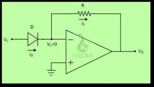
  2. Fan or Air Mover: The fan or air mover is responsible for generating the airflow in the wind tunnel. The size and type of fan depend on the wind tunnel’s design and the desired airspeed.

  3. Diffuser: The diffuser is a section of the wind tunnel that gradually widens the cross-sectional area of the airflow, reducing the velocity and increasing the pressure.

  4. Contraction: The contraction is a section of the wind tunnel that gradually narrows the cross-sectional area of the airflow, increasing the velocity and reducing the turbulence.

  5. Settling Chamber: The settling chamber is designed to remove any turbulence generated by the fan before the air enters the contraction.

Airflow Characterization and Measurement

The airflow in a wind tunnel is characterized by various parameters, including:

  1. Velocity: Velocity is measured using pitot tubes or hot-wire anemometers.
  2. Pressure: Pressure is measured using pressure transducers or pressure scanners.
  3. Temperature: Temperature is measured using thermocouples or resistance temperature detectors.
  4. Turbulence: Turbulence is measured using turbulence probes or laser Doppler anemometry.

The accuracy and quality of the wind tunnel flow are critical for obtaining reliable data. The flow quality is assessed using various parameters, including:

  1. Turbulence Intensity: The ratio of the root mean square of the fluctuating velocity to the mean velocity.
  2. Flow Uniformity: The degree of uniformity of the velocity across the test section.
  3. Flow Direction: The angle between the mean velocity vector and the longitudinal axis of the test section.

The acceptable values of these parameters depend on the type of wind tunnel and the object being tested.

Theoretical Considerations

The behavior of objects in a wind tunnel is governed by the principles of fluid dynamics, which can be described using various mathematical models and equations. Some key theoretical considerations include:

  1. Bernoulli’s Principle: This principle states that as the speed of a fluid increases, the pressure within the fluid decreases. This principle is fundamental to the study of aerodynamics and is used to explain the lift generated by airfoils.

  2. Boundary Layer Theory: The boundary layer is the thin layer of fluid adjacent to the surface of an object, where the effects of viscosity are significant. The behavior of the boundary layer, such as separation and transition, can have a significant impact on the overall aerodynamic performance of the object.

  3. Reynolds Number: The Reynolds number is a dimensionless quantity that represents the ratio of inertial forces to viscous forces in a fluid flow. It is an important parameter in the study of fluid dynamics and is used to determine the flow regime (laminar or turbulent) and the scaling of wind tunnel experiments.

  4. Computational Fluid Dynamics (CFD): CFD is a numerical technique used to simulate the behavior of fluids, including the airflow in wind tunnels. CFD can be used to complement wind tunnel experiments and provide additional insights into the flow phenomena.

Practical Applications and Considerations

Wind tunnels are used in a wide range of applications, including:

  1. Aerodynamic Design Optimization: Wind tunnels are used to test and optimize the aerodynamic performance of aircraft, automobiles, and other objects.
  2. Structural Load Evaluation: Wind tunnels are used to assess the impact of wind on buildings, bridges, and other structures, allowing engineers to design more resilient structures.
  3. Turbomachinery Testing: Wind tunnels are used to test the performance of turbines, compressors, and other turbomachinery components.
  4. Ballistics and Projectile Testing: Wind tunnels are used to study the behavior of projectiles, such as bullets and missiles, in high-speed airflow.

When conducting wind tunnel experiments, it is important to consider factors such as scale effects, model fidelity, and measurement uncertainty. Proper experimental design and data analysis techniques are crucial for obtaining reliable and meaningful results.

Conclusion

Wind tunnels are essential tools in the field of fluid dynamics and aerodynamics, providing researchers and engineers with the ability to study the behavior of objects in a controlled airflow environment. By understanding the various types of wind tunnels, their primary components, and the principles governing the airflow, scientists and engineers can leverage these facilities to optimize designs, evaluate performance, and assess the impact of wind on structures. The detailed overview presented in this article serves as a comprehensive guide for science students interested in the field of wind tunnel research and applications.

References

  1. Measurement and assessment of wind tunnel flow quality, 2008, ResearchGate.
  2. Wind Tunnel Flow Quality and Data Accuracy Requirements, 1985, DTIC.
  3. Wind Tunnels, an overview, ScienceDirect Topics.
  4. Toward a Standard on the Wind Tunnel Method, 2016, NIST.
  5. Uncertainty Quantification of Wind-tunnel Tests of a Low-Rise Building Model using the NIST Aerodynamic Database, 2021, TigerPrints.

A Detailed Overview on Jupiter, the Largest Planet

a detailed overview on jupiter the largest planet

Jupiter, the largest planet in our solar system, is a true giant, with a wealth of fascinating characteristics and a rich history of exploration. As the fifth planet from the Sun, Jupiter’s sheer size and complexity have captivated astronomers and scientists for centuries. In this comprehensive blog post, we’ll delve into the intricate details of this colossal world, exploring its physical properties, atmospheric features, magnetic field, and more.

Physical Characteristics

Jupiter’s immense size is truly staggering. With an equatorial diameter of 143,000 km (88,900 miles), it is over 11 times the diameter of Earth. Its mean distance from the Sun is 778,340,821 km (5.2 astronomical units), and its orbit has an eccentricity of 0.048 and an inclination of 1.3° to the ecliptic. The Jovian year, or the planet’s sidereal period of revolution, is 11.86 Earth years, and its visual magnitude at mean opposition is a striking -2.70.

Jupiter’s rapid rotation is another remarkable feature, with a mean synodic period of 398.88 Earth days and a mean orbital velocity of 13.1 km/sec. The planet’s equatorial radius is 71,492 km, while its polar radius is 66,854 km, indicating a significant oblate spheroid shape. Its mass is an astounding 18.98 × 10^26 kg, with a mean density of 1.33 g/cm^3 and a surface gravity of 2,479 cm/sec^2. The planet’s escape velocity is a staggering 60.2 km/sec.

Rotation Periods

a detailed overview on jupiter the largest planet

Jupiter’s rotation is complex, with three distinct systems:

  1. System I (±10° from Equator): 9 hr 50 min 30 sec
  2. System II (Higher Latitudes): 9 hr 55 min 41 sec
  3. System III (Magnetic Field): 9 hr 55 min 29 sec

This variation in rotation periods is a result of the planet’s dynamic atmospheric conditions and the complex interactions between its layers.

Magnetic Field and Magnetosphere

Jupiter’s magnetic field is incredibly powerful, with a strength of 4.3 gauss at the equator. This immense magnetic field, the largest in the solar system, creates a vast magnetosphere that extends millions of kilometers into space, trapping charged particles and creating a dynamic and complex environment.

Atmosphere

Jupiter’s atmosphere is primarily composed of hydrogen and helium, with the former making up approximately 90% of the composition. The planet’s cloud bands, which are visible from Earth, are created by cold, windy clouds of ammonia and water. One of the most famous features of Jupiter’s atmosphere is the Great Red Spot, a giant storm larger than Earth itself, with a diameter of about 16,350 km (10,159 miles).

Moons and Ring System

Jupiter has an extensive system of moons, with a total of 95 known satellites. The planet also has a main ring and three less-dense ring components, forming a complex and dynamic ring system.

Formation and Structure

Jupiter is believed to have formed from the dust and gases left over from the Sun’s formation, approximately 4.5 billion years ago. The planet’s core is partially dissolved, with no clear separation from the metallic hydrogen around it, leading researchers to describe it as “fuzzy.”

Exploration

Jupiter has been the subject of extensive exploration since the first detailed observations made by Galileo Galilei in 1610. The most recent mission to the planet is NASA’s Juno spacecraft, which has been studying the giant planet from orbit since 2016.

Additional Facts

  • Jupiter is the oldest planet in the solar system, having formed from the same dust and gases that gave rise to the Sun.
  • The planet has the shortest day in the solar system, with a rotation period of only 10.5 hours.
  • Despite its immense size and powerful gravitational field, Jupiter is unlikely to support life as we know it due to its extreme temperatures, pressures, and atmospheric composition.

References

  1. Britannica. (2024). Jupiter – Gas Giant, Moons, Orbit | Britannica. Retrieved from https://www.britannica.com/place/Jupiter-planet/Basic-astronomical-data
  2. NASA. (n.d.). Jupiter: Facts – NASA Science. Retrieved from https://science.nasa.gov/jupiter/jupiter-facts/
  3. NASA. (n.d.). Jupiter – NASA Science. Retrieved from https://science.nasa.gov/jupiter/
  4. PBS LearningMedia. (2016). Jupiter: The Largest Planet – PBS LearningMedia. Retrieved from https://thinktv.pbslearningmedia.org/resource/npls12.sci.ess.eiu.juplarge/jupiter-the-largest-planet/
  5. Space.com. (2023). Jupiter: A guide to the largest planet in the solar system – Space.com. Retrieved from https://www.space.com/7-jupiter-largest-planet-solar-system.html

A Detailed Overview on Venus, the Hottest Planet

a detailed overview on venus the hottest planet

Venus, the second planet from the Sun, is renowned for being the hottest planet in our solar system, with surface temperatures hot enough to melt lead. This comprehensive guide delves into the intricate details of Venus, providing a wealth of technical and advanced information for physics students and enthusiasts.

Physical Characteristics

Venus has a diameter of 12,100 km (7,520 miles), approximately 80% of Earth’s mass, and a density similar to Earth’s. The planet’s surface temperature is a staggering 480°C (900°F), primarily due to its atmospheric composition of 96% carbon dioxide, 3% nitrogen, and trace amounts of other gases.

The high surface temperature of Venus is a result of the greenhouse effect, where the planet’s dense atmosphere traps heat from the Sun, causing a runaway heating process. This effect is amplified by the presence of clouds composed of sulfuric acid and sulfur dioxide, which further contribute to the extreme temperatures.

Orbital and Rotational Characteristics

a detailed overview on venus the hottest planet

Venus orbits the Sun at a distance of 108 million km (67 million miles), taking 225 Earth days to complete one revolution around the Sun. However, the planet’s rotation is unique, as it spins slowly in the opposite direction from most other planets, with a length of day of 243 Earth days.

The retrograde rotation of Venus, where the planet spins in the opposite direction to its orbital motion, is a result of the planet’s early formation and the complex interactions between its gravitational forces and the solar system’s dynamics. This unique rotational characteristic has significant implications for the planet’s climate and atmospheric patterns.

Atmospheric Features

Venus’ atmosphere is remarkably dense, with a pressure over 90 times that of Earth’s, akin to the pressure experienced at a depth of 1,000 meters (3,300 feet) in the ocean. This extreme atmospheric pressure is a consequence of the planet’s high carbon dioxide content, which traps heat and creates the runaway greenhouse effect.

The clouds of Venus are composed primarily of sulfuric acid and sulfur dioxide, which contribute to the planet’s distinctive yellow-orange hue. These clouds play a crucial role in the greenhouse effect, as they effectively trap heat and prevent it from escaping the planet’s surface.

To quantify the atmospheric features, we can use the following equations:

  1. Atmospheric Pressure: The atmospheric pressure on Venus can be calculated using the barometric formula:
    P = P0 * e^(-m*g*h / (R*T))
    where P is the atmospheric pressure, P0 is the reference pressure, m is the molar mass of the atmosphere, g is the gravitational acceleration, h is the altitude, R is the universal gas constant, and T is the absolute temperature.

  2. Greenhouse Effect: The greenhouse effect on Venus can be quantified using the Stefan-Boltzmann law:
    Q = σ * A * (T^4 - T0^4)
    where Q is the heat flux, σ is the Stefan-Boltzmann constant, A is the surface area, T is the surface temperature, and T0 is the temperature of the surroundings.

These equations and their associated parameters provide a more technical and quantifiable understanding of Venus’ atmospheric characteristics.

Geological Features

The surface of Venus is dominated by volcanic plains and rifts, with thousands of volcanoes, some of which are still active. The planet’s crust is estimated to be 10 to 20 km (6 to 12 miles) thick, primarily composed of basalt.

Venus’ core is believed to be metallic, roughly 6,000 km (2,400 miles) wide, similar to Earth’s core structure. However, unlike Earth, Venus does not have an internally generated magnetic field. Instead, it has an induced magnetic field due to the interaction between the solar wind and the planet’s outer atmosphere.

To further understand the geological features of Venus, we can consider the following data points:

  • Surface Composition: Venus’ surface is primarily composed of basalt, with a silica content of around 50-55%.
  • Volcanic Activity: Venus has an estimated 1,600 major volcanoes, with some still actively erupting.
  • Tectonic Activity: The planet’s surface exhibits evidence of tectonic activity, such as rifts and faults, though the mechanisms are not fully understood.
  • Crater Density: The crater density on Venus is relatively low compared to other terrestrial planets, suggesting a younger, more geologically active surface.

These geological characteristics provide insights into the formation, evolution, and internal structure of Venus, which are crucial for understanding the planet’s unique features and potential for future exploration.

Exploration and Missions

Venus has been the subject of numerous exploration missions, with both successful and failed attempts to study the planet’s atmosphere, surface, and potential for life.

Some notable missions and their key findings include:

  1. VERITAS Mission (Planned): This NASA mission, scheduled for launch in the 2020s, aims to collect high-resolution, global maps of Venus’ surface to better understand its geological history and evolution.

  2. Davinci Mission (Planned): Another NASA mission, Davinci is designed to explore Venus’ atmosphere and surface, with the goal of providing insights into the planet’s formation and potential for habitability.

  3. Russian Venera Probes: The Soviet Union’s Venera program successfully landed several probes on the surface of Venus, detecting particles in the planet’s lower atmosphere that could be indicative of microbial life.

These missions, along with ongoing and future explorations, continue to expand our understanding of Venus and its unique characteristics, paving the way for further scientific discoveries and potential future human exploration.

Unique Features and Potential for Life

Venus stands out among the planets in our solar system due to its distinct features and the ongoing debate surrounding the potential for life on the planet.

One of the most notable characteristics of Venus is the lack of water on its surface. Unlike Earth, Venus is almost entirely devoid of water, which has significant implications for its geological history and the potential for life.

Another unique feature of Venus is its induced magnetic field, which is generated by the interaction between the solar wind and the planet’s outer atmosphere, rather than an internally generated magnetic field like Earth’s.

Despite the extreme surface conditions, the upper atmosphere of Venus, with temperatures ranging from 30°C to 70°C (86°F to 158°F), may potentially be habitable for extremophile microbes. Additionally, the persistent, dark streaks observed in the planet’s clouds have been a subject of ongoing investigation, as they could be indicative of microbial life or other chemical compounds.

To further explore the potential for life on Venus, scientists have proposed various hypotheses and experiments, such as:

  1. Cloud Habitability: Investigating the possibility of extremophile microbes thriving in the upper atmospheric conditions of Venus.
  2. Atmospheric Chemistry: Analyzing the chemical composition of the clouds and their potential to support life.
  3. Subsurface Habitats: Exploring the possibility of microbial life in the planet’s subsurface, where conditions may be more favorable.

These unique features and the ongoing exploration of Venus’ potential for life continue to captivate the scientific community and drive further research and missions to unravel the mysteries of this enigmatic planet.

References:

  1. NASA Science. (n.d.). Venus. Retrieved from https://science.nasa.gov/venus/
  2. NASA Science. (n.d.). Venus: Facts. Retrieved from https://science.nasa.gov/venus/venus-facts/
  3. Exploring the Planets. (n.d.). Chapter 7. Venus. Retrieved from https://explanet.info/Chapter07.htm
  4. Space.com. (2024). Venus facts — A guide to the 2nd planet from the sun. Retrieved from https://www.space.com/44-venus-second-planet-from-the-sun-brightest-planet-in-solar-system.html
  5. UCL Culture Online. (2022). Is Venus the hottest planet? Retrieved from https://www.ucl.ac.uk/culture-online/case-studies/2022/sep/venus-hottest-planet
  6. Sagan, C. (1961). The Planet Venus. Annual Review of Astronomy and Astrophysics, 1(1), 39-58.
  7. Kasting, J. F. (1988). Runaway and moist greenhouse atmospheres and the evolution of Earth and Venus. Icarus, 74(3), 472-494.
  8. Smrekar, S. E., & Stofan, E. R. (1997). Corona formation and heat loss on Venus. Science, 277(5330), 1289-1294.
  9. Grinspoon, D. H. (1997). Venus revealed: A new look below the clouds of our mysterious twin planet. Addison-Wesley.
  10. Gilmore, M. S., & Treiman, A. H. (2021). The Geology of Venus: Progress, Puzzles, and Future Directions. Annual Review of Earth and Planetary Sciences, 49, 1-30.

The Non-Inverting Op-Amp Voltage Follower: A Comprehensive Guide

non inverting op amp voltage follower

The non-inverting op-amp voltage follower, also known as a unity gain buffer, is a specific configuration of the non-inverting amplifier circuit that provides a high input impedance and low output impedance, effectively buffering the input signal and preventing the loading effect in multi-stage circuits.

Understanding the Non-Inverting Op-Amp Voltage Follower

The non-inverting op-amp voltage follower has a gain of 1, meaning the output voltage (Vout) is equal to the input voltage (Vin). This is because the feedback resistor (Rf) is not present in this configuration, and the input resistor (Rin) is connected directly to the non-inverting input of the operational amplifier.

Key Characteristics of the Voltage Follower

  1. Input Impedance: The input impedance of the non-inverting op-amp voltage follower is high due to the direct connection to the op-amp’s non-inverting input. This high input impedance ensures minimal loading on the input signal source, preventing the input signal from being attenuated or distorted.

  2. Output Impedance: The output impedance of the voltage follower is low, allowing it to drive loads effectively. This low output impedance is a crucial characteristic that enables the voltage follower to maintain the input signal’s integrity when connected to various loads.

  3. Phase Shift: There is no phase shift between the input and output signals in the non-inverting op-amp voltage follower. The voltage follower maintains the same phase, ensuring that the output signal is in phase with the input signal.

  4. Current Transfer: The current transfer from the input to the output of the voltage follower is nearly ideal, with minimal loading effect on the input signal source. This means that the current drawn from the input source is negligible, preserving the input signal’s integrity.

Theoretical Analysis of the Voltage Follower

The non-inverting op-amp voltage follower can be analyzed using the following formula:

Vout = Vin * (1 + Rf/Rin)

For a voltage follower, the feedback resistor (Rf) is not present, so the formula simplifies to:

Vout = Vin * (1 + 0)
Vout = Vin

This confirms that the output voltage is equal to the input voltage, making the voltage follower a useful circuit for buffering signals.

Practical Applications of the Non-Inverting Op-Amp Voltage Follower

non inverting op amp voltage follower

The non-inverting op-amp voltage follower finds numerous applications in various electronic circuits and systems, including:

  1. Signal Buffering: The voltage follower is commonly used to buffer signals, preventing the loading effect and maintaining the integrity of the input signal. This is particularly important in multi-stage circuits, where the output of one stage needs to be connected to the input of the next stage without affecting the signal.

  2. Impedance Matching: The voltage follower’s high input impedance and low output impedance make it useful for impedance matching between different circuit components or stages. This ensures efficient power transfer and minimizes signal reflections.

  3. Analog-to-Digital Conversion: In analog-to-digital conversion (ADC) systems, the voltage follower is often used to provide a low-impedance source for the ADC, ensuring accurate and stable voltage measurements.

  4. Sensor Interfacing: When interfacing sensors with electronic circuits, the voltage follower can be used to buffer the sensor’s output, preventing the sensor from being loaded by the subsequent circuitry.

  5. Driving Capacitive Loads: The voltage follower’s low output impedance allows it to effectively drive capacitive loads, such as long cables or high-capacitance inputs, without introducing significant phase shifts or signal distortion.

  6. Isolation and Protection: The voltage follower can be used to isolate sensitive circuits from external disturbances or high-current loads, providing protection and preventing damage to the sensitive components.

Example Numerical Problem

Consider an input voltage (Vin) of 2V applied to a non-inverting op-amp voltage follower with an input resistance (Rin) of 10 kΩ. Calculate the output voltage (Vout).

Using the voltage follower formula:

Vout = Vin * (1 + Rf/Rin)

Since Rf is not present in this configuration:

Vout = Vin * (1 + 0)
Vout = Vin
Vout = 2V

In this example, the output voltage (Vout) is equal to the input voltage (Vin) of 2V, as expected for a non-inverting op-amp voltage follower.

Conclusion

The non-inverting op-amp voltage follower is a versatile and widely used circuit configuration in electronic systems. Its ability to provide high input impedance, low output impedance, and unity gain makes it an essential building block for various applications, including signal buffering, impedance matching, analog-to-digital conversion, sensor interfacing, and driving capacitive loads. Understanding the characteristics and theoretical analysis of the voltage follower is crucial for designing and implementing effective electronic circuits.

Reference:

  1. MIT OpenCourseWare: Introduction to Electronics, Signals, and Measurement
  2. Electronics Tutorials: Op-Amp Voltage Follower
  3. Jake Electronics: Operational Amplifiers – Inverting vs. Non-Inverting Op-Amps