The Comprehensive Guide to Laser Microphones: A Hands-on Exploration

laser microphone

Laser microphones are a remarkable technological advancement that utilizes the principles of laser optics and vibration detection to remotely capture audio signals. These devices employ a laser beam to detect minute surface vibrations, allowing for the remote monitoring and recording of sound without the need for physical contact with the target. This comprehensive guide will delve into the intricate details of laser microphone technology, providing a wealth of technical information and practical insights for science students and enthusiasts.

Understanding the Fundamentals of Laser Microphones

At the core of a laser microphone is the ability to detect and measure the deflection or wobble of a reflected laser beam. When a laser beam is directed at a surface, such as a window or a wall, the surface vibrations caused by sound waves will modulate the reflected beam. By analyzing the changes in the reflected beam, the original audio signal can be recovered and reproduced.

Laser Types and Characteristics

The choice of laser used in a laser microphone is crucial, as it determines the performance and capabilities of the system. Common laser types employed in these devices include:

  1. Helium-Neon (HeNe) Lasers: HeNe lasers are known for their stability, coherence, and relatively high power output, making them a popular choice for laser microphones. These lasers typically operate at a wavelength of 632.8 nm and can provide up to 50 mW of power.

  2. Diode Lasers: Diode lasers are compact, efficient, and cost-effective alternatives to HeNe lasers. They are available in a wide range of wavelengths, from visible to near-infrared, and can deliver power outputs ranging from milliwatts to several watts.

  3. Frequency-Doubled Neodymium-Doped Yttrium Aluminum Garnet (Nd:YAG) Lasers: Nd:YAG lasers are known for their high power and excellent beam quality. By frequency-doubling the output of an Nd:YAG laser, it is possible to obtain a green laser with a wavelength of 532 nm, which can be advantageous for certain laser microphone applications.

The choice of laser type depends on factors such as power output, wavelength, beam quality, and cost, as well as the specific requirements of the laser microphone application.

Optical Detectors and Demodulation Techniques

To capture the modulated laser beam and extract the audio signal, laser microphones employ optical detectors, such as photodiodes or phototransistors. These devices convert the received light into an electrical signal, which can then be processed and analyzed.

The demodulation technique used to recover the audio signal from the electrical signal is crucial. One common method is the use of a lock-in amplifier, which synchronizes to the modulation frequency of the laser and extracts the signal of interest. Other techniques include phase-sensitive detection and homodyne detection, each with its own advantages and trade-offs.

Sensitivity and Range Considerations

The sensitivity of a laser microphone is influenced by several factors, including the power output of the laser, the sensitivity of the optical detector, and the signal-to-noise ratio of the system. Laser microphones can be more sensitive than traditional microphones, as they can detect very small vibrations in the target surface.

The range of a laser microphone is determined by the power output of the laser, the sensitivity of the optical detector, and the reflectivity of the target surface. Laser microphones can operate at longer ranges than traditional microphones, as the laser beam can be focused to a small spot and the reflected beam can be detected over long distances.

Laser Microphone Design and Optimization
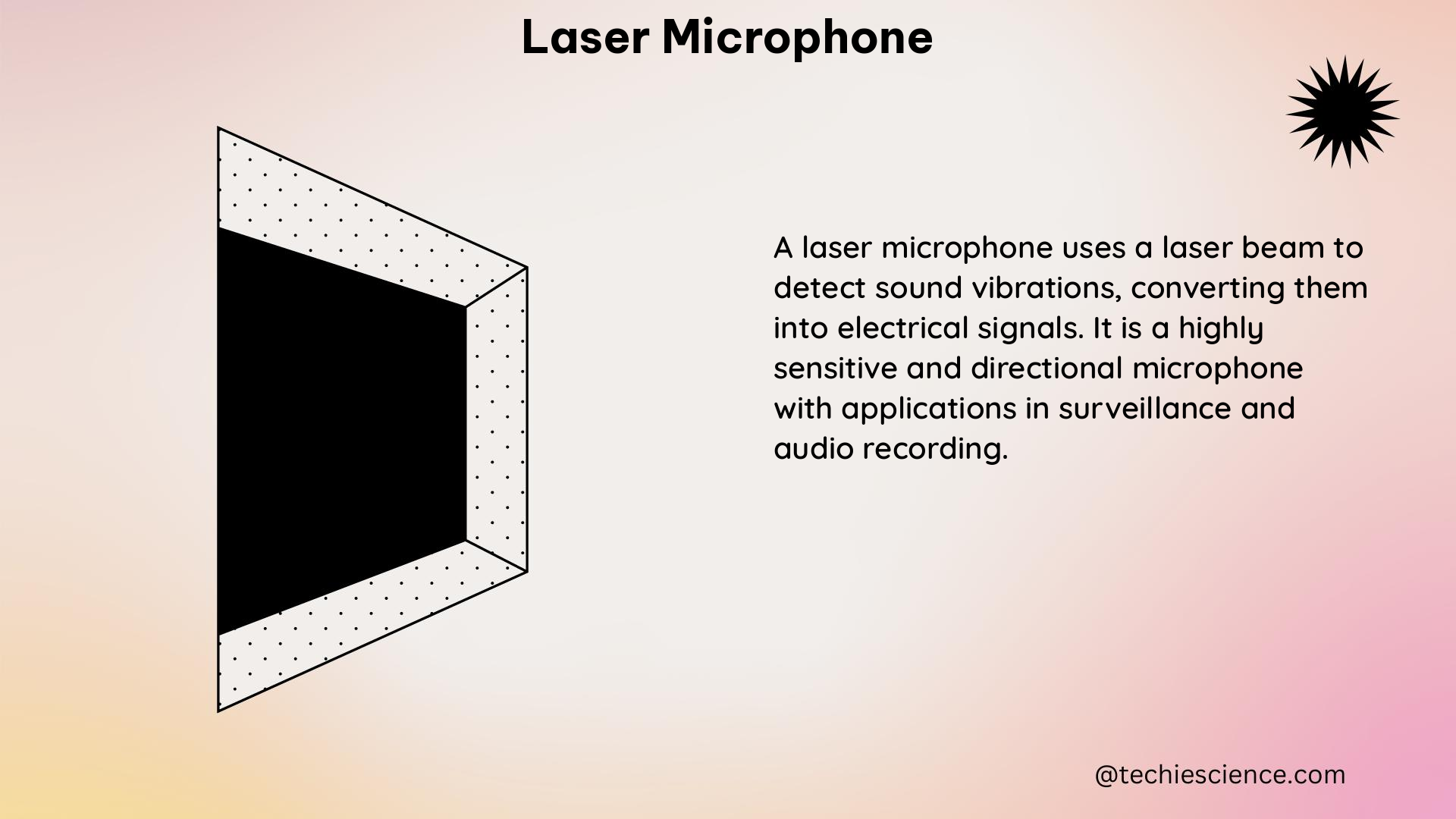
laser microphone

Designing an effective laser microphone requires careful consideration of various parameters and optimization techniques. Let’s explore some key aspects of laser microphone design:

Laser Beam Characteristics

The characteristics of the laser beam, such as its power, wavelength, and beam quality, play a crucial role in the performance of a laser microphone. Higher laser power can improve the signal-to-noise ratio, while the choice of wavelength can affect the sensitivity and interference susceptibility of the system.

The beam quality, as measured by the beam parameter product (BPP) or M^2 factor, determines the ability to focus the laser beam to a small spot, which is essential for maximizing the sensitivity and range of the laser microphone.

Optical System Design

The optical system of a laser microphone is responsible for directing the laser beam to the target surface and collecting the reflected beam. This system typically includes lenses, mirrors, and other optical components to collimate, focus, and steer the laser beam.

The design of the optical system must consider factors such as beam divergence, focal length, and the placement of the optical components to optimize the performance of the laser microphone.

Demodulation and Signal Processing

The demodulation and signal processing techniques used in a laser microphone are critical for extracting the audio signal from the modulated laser beam. The choice of demodulation method, such as lock-in amplification or homodyne detection, depends on the specific requirements of the application and the characteristics of the target surface.

Signal processing algorithms, including filtering, amplification, and noise reduction, can further enhance the quality of the recovered audio signal.

Interference Mitigation

Laser microphones can be susceptible to interference from other light sources, such as sunlight or artificial lighting. To minimize the impact of interference, the laser beam can be modulated at a high frequency, which can reduce the influence of ambient light.

Additionally, the use of narrow-band optical filters and careful shielding of the optical components can help to improve the signal-to-noise ratio and reduce the impact of interference.

Practical Applications and Considerations

Laser microphones have found various applications in fields such as security, surveillance, and scientific research. Let’s explore some practical considerations and use cases for these devices:

Security and Surveillance

Laser microphones can be used for remote eavesdropping and surveillance applications, as they can capture audio signals from a distance without the need for physical access to the target. This makes them valuable tools for security and intelligence gathering operations.

However, the use of laser microphones for surveillance purposes raises ethical and legal concerns, and their deployment must be carefully considered and regulated.

Scientific Research and Instrumentation

Laser microphones have found applications in scientific research and instrumentation, where their high sensitivity and non-contact nature make them valuable tools for vibration analysis, acoustic measurements, and other applications.

For example, laser microphones can be used in the calibration of traditional microphones, as they can provide a more accurate reference signal for the measurement of sound pressure levels.

Challenges and Limitations

While laser microphones offer several advantages, they also face some challenges and limitations. These include:

  1. Sensitivity to Environmental Conditions: Laser microphones can be sensitive to environmental factors such as temperature, humidity, and air turbulence, which can affect the stability and accuracy of the system.

  2. Complexity and Cost: Laser microphone systems can be more complex and costly to design and build compared to traditional microphones, which may limit their widespread adoption in certain applications.

  3. Regulatory Considerations: The use of laser technology in microphones may be subject to regulatory requirements and safety guidelines, which must be carefully considered and addressed.

Conclusion

Laser microphones represent a remarkable technological advancement in the field of audio sensing and remote monitoring. By leveraging the principles of laser optics and vibration detection, these devices offer unique capabilities and advantages over traditional microphones, such as increased sensitivity, extended range, and non-contact operation.

This comprehensive guide has explored the technical details and practical considerations of laser microphones, providing a wealth of information for science students and enthusiasts. From understanding the fundamental components and design principles to exploring practical applications and limitations, this guide aims to equip readers with a deep understanding of this fascinating technology.

As laser microphone technology continues to evolve, the potential for innovative applications and further advancements remains vast. By delving into the intricacies of laser microphones, readers can gain valuable insights and inspire future developments in this exciting field of science and engineering.


References

  1. Laser Microphone Project
  2. Testing 1-2: New Laser-Based Microphone Calibration Measures Up
  3. Laser Doppler Vibrometry Brings More Accurate Microphone Calibration
  4. Laser Microphone: Principles, Design, and Applications
  5. Laser Microphone Technology: A Review
  6. Laser Microphone for Remote Acoustic Sensing

Laser Beam Welding: A Comprehensive Guide for Science Students

laser beam welding

Laser beam welding (LBW) is a highly precise welding technique that utilizes a concentrated laser beam to melt and fuse materials. The process involves several key measurable and quantifiable parameters that can significantly impact the quality and consistency of the weld, including laser power, beam diameter, welding speed, and focal position.

Laser Power Measurement: Ensuring Consistent Weld Quality

Laser power is a critical parameter in LBW, as it directly influences the amount of energy delivered to the workpiece. Measuring laser power accurately is essential for ensuring consistent weld quality. Traditional thermal power meters, which measure heat delivery, are commonly used for this purpose. However, these methods may not be suitable for real-time power measurement during the welding process.

To address this challenge, researchers at the National Institute of Standards and Technology (NIST) have developed a novel optical laser-power measurement technique that allows for high accuracy in real-time measurements. This technique measures the force of light, or radiation pressure, exerted by the laser beam on a sensitive scale, providing a direct and accurate measurement of laser power during the welding process.

The radiation pressure exerted by a laser beam can be calculated using the following formula:

F = 2P/c

Where:
F is the radiation pressure (in newtons)
P is the laser power (in watts)
c is the speed of light (approximately 3 × 10^8 m/s)

By measuring the force exerted by the laser beam on a sensitive scale, researchers can accurately determine the laser power in real-time, enabling precise control and monitoring of the welding process.

Beam Diameter Measurement: Optimizing Energy Density and Penetration Depth

laser beam welding

Beam diameter is another critical parameter in LBW, as it affects the energy density and penetration depth of the laser beam. Measuring the beam diameter accurately is essential for ensuring consistent weld quality. High-speed imaging analysis of laser welding processes has shown that new methods are being developed to collect quantitative measurements of the laser weld process with high-speed cameras.

One such method involves the use of a high-speed camera to capture the laser beam profile during the welding process. By analyzing the captured images, researchers can measure the beam diameter and other critical parameters, such as the beam shape and intensity distribution, in real-time. This information can be used to optimize the laser beam parameters and improve the overall quality of the weld.

The beam diameter can be calculated using the following formula:

d = 2w

Where:
d is the beam diameter (in meters)
w is the beam radius (in meters)

By accurately measuring the beam diameter, welding engineers can ensure that the energy density and penetration depth of the laser beam are optimized for the specific application, leading to improved weld quality and consistency.

Welding Speed Measurement: Controlling Heat Input and Cooling Rate

Welding speed is another important parameter in LBW, as it affects the heat input and cooling rate of the weld. Measuring welding speed accurately is essential for ensuring consistent weld quality. Process monitoring and control of laser beam welding can be facilitated through measurement of quantifiable variables, such as welding speed, to improve processing results.

One method for measuring welding speed involves the use of high-speed cameras or laser displacement sensors to track the movement of the workpiece or the laser beam itself. By analyzing the captured data, researchers can calculate the welding speed and use this information to optimize the process parameters.

The welding speed can be calculated using the following formula:

v = d/t

Where:
v is the welding speed (in meters per second)
d is the distance traveled by the workpiece or laser beam (in meters)
t is the time taken to travel the distance (in seconds)

By accurately measuring the welding speed, welding engineers can control the heat input and cooling rate of the weld, ensuring consistent weld quality and reducing the risk of defects.

Focal Position Measurement: Optimizing Energy Density and Penetration Depth

Focal position is the final critical parameter in LBW, as it affects the energy density and penetration depth of the laser beam. Measuring the focal position accurately is essential for ensuring consistent weld quality. Closed-loop power and focus control of laser welding for full-penetration monitoring has been shown to improve weld quality and reduce defects.

One method for measuring the focal position involves the use of a laser displacement sensor or a confocal sensor to track the position of the laser beam relative to the workpiece. By analyzing the captured data, researchers can determine the focal position and use this information to adjust the laser beam parameters accordingly.

The focal position can be calculated using the following formula:

f = z - z_0

Where:
f is the focal position (in meters)
z is the distance between the laser source and the workpiece (in meters)
z_0 is the focal length of the laser beam (in meters)

By accurately measuring the focal position, welding engineers can optimize the energy density and penetration depth of the laser beam, leading to improved weld quality and reduced defects.

Conclusion

Laser beam welding involves several critical measurable and quantifiable parameters, including laser power, beam diameter, welding speed, and focal position. Accurate measurement and control of these parameters are essential for ensuring consistent weld quality and improving processing results. New methods and techniques, such as high-speed imaging analysis and radiation pressure measurement, are being developed to improve the accuracy and efficiency of these measurements.

By understanding and applying these advanced measurement techniques, science students and welding engineers can optimize the laser beam welding process, leading to improved productivity, reduced defects, and enhanced weld quality.

References:

  1. Laser Welding Parameter – an overview | ScienceDirect Topics
  2. High speed imaging analysis of laser welding – Diva-Portal.org
  3. Measuring Laser Beam Welding Power Using the Force of Light – NIST
  4. Process Monitoring and Control of Laser Beam Welding: Measuring Quantifiable Data for Improved Processing Results

The Comprehensive Guide to Laser Etching: A Hands-on Playbook for Science Students

laser etching

Laser etching is a highly precise and versatile technique that allows for the creation of permanent markings on a wide range of materials, including metals, plastics, and ceramics. By precisely controlling the energy delivered by a laser beam, this process can produce intricate designs, serial numbers, barcodes, and logos with exceptional accuracy and durability. This comprehensive guide will delve into the technical details of laser etching, providing science students with a hands-on playbook to master this advanced manufacturing process.

Understanding the Fundamentals of Laser Etching

Laser etching is a non-contact, subtractive manufacturing process that utilizes a focused laser beam to selectively remove material from the surface of a workpiece. The laser beam, typically generated by a CO2 or fiber laser, delivers a high amount of energy to a small, targeted area, causing the material to melt and vaporize. This localized melting and expansion of the material results in the creation of permanent markings on the surface.

The key parameters that govern the laser etching process are:

  1. Laser Power: The power of the laser beam, typically measured in watts (W), determines the amount of energy delivered to the material. Higher laser power can result in deeper and more pronounced etchings.

  2. Pulse Duration: The duration of each laser pulse, measured in microseconds (μs), affects the depth and width of the etching. Shorter pulses can create finer, more detailed markings.
  3. Pulse Frequency: The number of laser pulses per second, measured in hertz (Hz), influences the speed and quality of the etching process. Higher pulse frequencies can lead to faster processing times.

  4. Beam Spot Size: The diameter of the focused laser beam, typically measured in micrometers (μm), determines the resolution and precision of the etching. Smaller beam spot sizes can produce more detailed markings.
  5. Scan Speed: The speed at which the laser beam moves across the material’s surface, measured in millimeters per second (mm/s), affects the depth and quality of the etching. Slower scan speeds can result in deeper and more uniform markings.
Controlling the Etching Process: Line Interval and DPI

laser etching

The size and appearance of the markings created through laser etching are primarily determined by two key settings: line interval and DPI (dots per inch).

Line Interval

The line interval, measured in micrometers (μm), refers to the distance between the individual lines or passes of the laser beam. A smaller line interval results in a higher density of lines, leading to a more uniform and continuous appearance of the etching.

The line interval can be calculated using the following formula:

Line Interval = Beam Spot Size / (DPI / 25.4)

Where:
– Beam Spot Size is the diameter of the focused laser beam, measured in micrometers (μm)
– DPI is the desired dots per inch of the etching

DPI (Dots per Inch)

The DPI setting determines the number of individual dots or pixels that make up the etching per inch of the material’s surface. A higher DPI value results in a higher resolution and more detailed markings, but it also requires a smaller line interval to avoid overlapping of the laser passes.

The relationship between line interval and DPI can be expressed as:

DPI = 25.4 / Line Interval

Where:
– Line Interval is the distance between the individual lines of the etching, measured in micrometers (μm)
– 25.4 is the conversion factor from micrometers to inches

It is important to find the optimal balance between line interval and DPI to achieve the desired quality and appearance of the etching without causing overburning or damage to the material.

Laser Beam Characteristics and Energy Delivery

The laser beam used in the etching process is a critical component that determines the quality and precision of the markings. Pulsed lasers, such as CO2 or fiber lasers, are commonly used in laser etching applications due to their ability to deliver high-energy pulses with precise control.

Pulsed Laser Characteristics

  • Pulse Energy: The amount of energy contained in each laser pulse, typically measured in millijoules (mJ).
  • Pulse Duration: The duration of each laser pulse, typically in the range of microseconds (μs) to nanoseconds (ns).
  • Pulse Frequency: The number of laser pulses per second, measured in hertz (Hz).
  • Peak Power: The maximum power of the laser pulse, calculated by dividing the pulse energy by the pulse duration, typically in the range of kilowatts (kW) to megawatts (MW).

The energy delivered by each laser pulse is absorbed by the material, causing it to heat up and melt. This localized melting and expansion of the material result in the creation of permanent markings on the surface.

Energy Absorption and Material Interaction

The interaction between the laser beam and the material being etched is a complex process that involves several physical phenomena, including:

  1. Optical Absorption: The material’s ability to absorb the laser energy, which is influenced by factors such as the wavelength of the laser, the material’s optical properties, and the surface condition.

  2. Thermal Conduction: The transfer of heat within the material, which can affect the depth and width of the etching.

  3. Phase Transitions: The changes in the material’s physical state, such as melting and vaporization, which occur due to the high-energy input from the laser.

  4. Plasma Formation: The ionization of the material’s surface, which can occur at high laser intensities and can influence the etching process.

Understanding these material-laser interactions is crucial for optimizing the laser etching process and achieving the desired results.

Laser Etching Techniques and Applications

Laser etching can be employed in a wide range of applications, from industrial manufacturing to consumer products. Some of the common techniques and applications include:

Techniques

  1. Raster Scanning: The laser beam is scanned across the material’s surface in a raster pattern, creating a series of parallel lines to form the desired marking.
  2. Vector Scanning: The laser beam follows a predefined vector path, allowing for the creation of more complex designs and shapes.
  3. Mask Projection: A mask or stencil is used to selectively expose the material to the laser beam, enabling the creation of multiple markings simultaneously.

Applications

  1. Industrial Marking: Laser etching is widely used for marking serial numbers, barcodes, and other identification codes on metal parts, tools, and equipment.
  2. Product Branding: Logos, graphics, and other branding elements can be permanently etched onto consumer products, such as electronics, jewelry, and sporting goods.
  3. Medical Device Marking: Laser etching is used to mark medical devices, implants, and surgical instruments with unique identifiers for traceability and patient safety.
  4. Art and Engraving: The precision and control of laser etching make it a popular technique for creating intricate designs, patterns, and engravings on a variety of materials.
  5. Semiconductor Packaging: Laser etching is employed in the semiconductor industry for marking and identification of integrated circuits, wafers, and other electronic components.

Emissions and Environmental Considerations

While laser etching is a highly efficient and precise manufacturing process, it is important to consider the potential environmental impact, particularly the emissions generated during the process.

A study on the characterization of emissions from carbon dioxide laser cutting activities found that there was a significant increase in total particulate concentrations during the post-background period after the laser cutting had been completed and the fume exhaust was turned off. The concentration of each method was an average of two laser cutting trials, with all six individual trial data presented in the study.

An ANOVA statistical test was used to determine that there was a significant difference between the total concentration means of each phase of laser cutting activities, with a follow-up t-test determining that there were only significant differences between the total background and post-background concentrations in Methods 2 and 3.

To mitigate the potential environmental impact of laser etching, it is essential to implement appropriate engineering controls, such as effective fume extraction systems and proper ventilation, to capture and contain the emissions generated during the process. Additionally, regular monitoring and testing of air quality in the work environment can help ensure compliance with relevant environmental regulations and safeguard the health and safety of workers.

Conclusion

Laser etching is a highly versatile and precise manufacturing process that allows for the creation of permanent markings on a wide range of materials. By understanding the fundamental principles of laser-material interactions, the importance of line interval and DPI settings, and the potential environmental considerations, science students can develop a comprehensive understanding of this advanced technique.

This hands-on playbook has provided a detailed overview of the technical aspects of laser etching, equipping you with the knowledge and tools necessary to effectively apply this process in various scientific and industrial applications. As you continue to explore and experiment with laser etching, remember to prioritize safety, environmental sustainability, and the pursuit of innovative solutions that push the boundaries of what is possible.

References

  1. Understanding line interval/DPI for engraving – Community Laser Talk. (2020-03-12). Retrieved from https://forum.lightburnsoftware.com/t/understanding-line-interval-dpi-for-engraving/13110
  2. Characterization of Emissions from Carbon Dioxide Laser Cutting Activities. (2023-06-22). Retrieved from https://www.ncbi.nlm.nih.gov/pmc/articles/PMC10369487/
  3. Laser Etching: Everything You Need to Know – Laserax. (2020-08-04). Retrieved from https://www.laserax.com/blog/laser-etching
  4. Laser Etching Fundamentals: A Comprehensive Guide. (2022-09-15). Retrieved from https://www.lasermech.com/blog/laser-etching-fundamentals
  5. Laser Etching Techniques and Applications. (2021-11-30). Retrieved from https://www.troteclaser.com/en/knowledge-base/laser-etching-techniques-and-applications/

Diode:It’s Working Principle,Types,7 Important Applications

Picture1 300x235 1

C O N T E N T S

  • Definition
  • Diode symbol
  • Important features
  • Biasing technique of Diodes
  • Important Types
  • Applications of Diodes

What are Diodes?

Definition of Diode:

“A diode is a special electronic element with two electrodes termed as the Anode and the Cathode”.

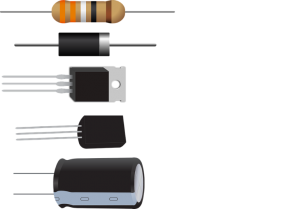
Different types of diodes


Most of the diodes are made of semiconductors such as silicon, germanium, or selenium.

How does a Diode function?

Working Principle of diode:

The basic characteristics of a diode is to carry electric current in only one direction. If the cathode is negatively charged at a voltage greater than the anode, a certain current called ‘forward break over’ starts flowing through it.

When the cathode is +ve charged in respect of the anode, it will not conduct any current. These can be operated as a rectifiers, switches and limiters.

The forward break over voltage is approximately 0.6 Volt for silicon, 0.3 Volt for germanium and 1 Volt for selenium material respectively.

At the forward break over point, if an analog signal flow through the diode the signal waveform is inaccurate and distorting. All the signals that get generated are harmonic and integral multiples if the input frequency. These generally produce signals at microwave frequency with the correct level and polarity of voltage application.

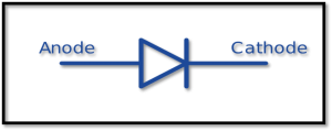
Symbol of Diode:

Diode
Diode Symbol

Important features of Diodes:

  • Diode is a two terminal electronic component
  • It has lower resistance in one direction and higher in another direction
  • Most of the diodes are made of silicon
  • The voltage drop under a forward bias condition is 0.7 volts approximately.
  • In the reverse biasing the region of depletion layer, will increase.

Different types of diode:

1.   P-N junction diode –

“A diode is a P-N junction with P-type on one side and N-type on the other side”.

2.   Light Emitting Diode (LED) –

“LED is a semiconductor light source that emits light when current flows through it”.

3.   Photo Diode –

This is a semiconductor-based P-N junction diode, if exposed to light produce a potential difference

4.   Schottky Diode –

 This is designed by the junction of a semiconductor with a metal. Sometime known as hot carrier diode”.

5.   Tunnel Diode –

A semiconductor diode that has effectively negative resistance due to the tunnelling”.

6.   Varactor diode –

 A diode with changing internal capacitance with the changes of the reverse voltage”.

7.   Zener Diode –

A special type of diode, designed to allow current to carry backwards when a reverse voltage is applied”.

What are the Ideal Diodes?

In an ideal diode, when it is in forward bias the current starts flowing freely from the device. In an ideal one usually without voltage drop when forward biased. All the other voltage sources are dropped across the circuit resistors. When reverse biased, in an ideal diode there is zero current flow and will have infinite resistance.

What are Practical Diodes?

In a practical diode, some of the resistances allow the current to flow if forward bias. Due to the presence of the resistances, some power is dissipated when the current starts flowing through the forward biased. When it’s in reverse biased, due to the high resistance it can conduct.

A diode is normally is P-N junction.

  1. It is a barrier potential. To overcome this problem by applying an extra voltage to the p-n junction, it can be able to conduct.
  2. So current will pass through p-n junction when the barrier potential is omitted.
  3. It is with two metallic conducts is known as p-n junction.
  4. The process of external voltage applying is channel biasing.

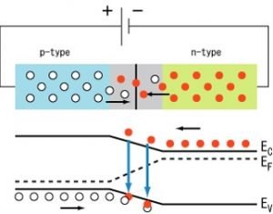
Forward Bias:

Picture1
Diode in Forward Biasing
Image Credit:  S-kei , PnJunction-Diode-ForwardBiasCC BY-SA 2.5
  • A battery connected +ve terminal to p-side of p-n junction diode & then connect -ve terminal to the n side.
  • If we apply an external voltage which is greater than the potential barrier then it starts conducting the current to pass
  • The diode is connected to a DC voltage source (V)
  • The voltage across the diode is called forward characteristic of p-n junction diode
  • No diode current flows till A is reached because external voltage Vf  is being opposed by built in voltage whose value is 0.
  • However voltage increases beyond A and the diode current decreases rapidly.
  • If the forward current is externally backward it cuts the voltage axis at a point from which Vk can be determined

Reverse Bias:

PnJunction Diode ReverseBias
Diode in Reverse biasing
Image Credit: S-keiPnJunction-Diode-ReverseBiasCC BY-SA 2.5
  • If voltage is applied to p-n junction diodes –ve terminal is connected to the p-type semiconductor. Similarly, +ve terminal is connected to the n-type.
  • Holes from p-side are attracted towards the -ve terminal. Whereas the free electrons from n-side are attracted towards +ve terminal.
  • The reverse bias increases in steps and diode current is observed.
  • When the reverse bias increases VBR the diode reverse current increases very shortly.

Switching property of diodes:

In forward bias when a small voltage is applied the diode conducts which exceeds the cut in voltage known as on-state.

In reverse bias only small voltage current sources with reverse applied voltage that is less than the breakdown value is known as off-state

In switching property of a diode is switched from forward bias on-state to reverse bias off-state or vice versa.

Applications of a diodes

Rectification:

A diode is usually acting as a rectifier, flattening an AC power source into a constant power supply. This can achieve this task by obstructive the flow in one direction and pass through the other direction.

Light emission:  

LED provides a much more efficient source of light. The bulbs are cost more than their incandescent counterparts, in part because they require additional control circuitry to work with AC power.

Inductive Load Dissipation:

Diodes are used in this application, when an inductive load is switched off, the energy it has stored must go somewhere. Without the proper circuit protection, the stored energy can lead to voltage spikes that can arc across the switch and potentially overload a transistor this configuration allows the current to dissipate across the inductor and it feeds back into the power supply and protects the circuit.

Sensing and Control:

Semiconductors can easily generate electrical charges based on the optical effects. In general, these devices are packaged in such a way that it blocks out light to avoid unintended electrical activity. Photodiodes are built to optimize this effect. These photodiodes are often used in the infrared spectrum, such as inside consumer remote controls.

For more Electronics related article click here

Bridge Rectifier, Circuit, Formula,7 Important Factors

1920px Diode bridge alt 1.svg 300x125 1

List of Topics

  • Rectification & Rectifier
  • Types of Rectifier
  • Bridge Rectifier
  • Bridge Rectifier Circuit and Diagram
  • Working of a bridge rectifier
  • Differences between Bridge Rectifier and Full Wave Rectifier
  • Mathematical problems

Rectification

Rectification: The process through which AC voltage is converted into Dc voltage is known as the rectification. Rectifier is the electronics device to perform the rectification

Types of Rectifiers

Rectifiers are mainly three types. They are –

  1. Half-Wave Rectifiers (HWR)
  2. Full-Wave Rectifiers (FWR)
  3. Bridge Rectifier (BR)

Bridge Rectifiers

Bridge rectifiers are kind of rectifiers that converts ac to dc that is alternating current to direct current. This type of rectifier allows both halves of the ac input voltage to pass through the circuit. Four diodes are necessary to make a bridge rectifier.

Bridge Rectifiers Working & Circuit

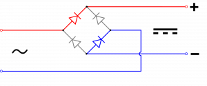
A bridge rectifier is shown in the below circuit.

1920px Diode bridge alt 1.svg
Bridge Rectifier Circuit Diagram, Image Source – User:WykisDiode bridge alt 1, marked as public domain, more details on Wikimedia Commons

Full-wave rectification can also be implemented with the help of a rectifiers, which includes four diodes. As shown in the circuit, two diodes of the opposite arms conduct current simultaneously while the other two diodes remained in OFF state. For Now, the current flows through the diode D1 and D3 but no current flows through the D2 and D4 diodes. This happens because of the instantaneous polarity of the secondary windings of the transformer.  A current I thus pass through the load resistance RL in the shown direction.

Now, the next half of the cycle comes. This time the transformer’s polarity changes. Current flows through the Diode D2 and diode D4 and no current flows through the diodes D1 and D3. The direction of flow of current remains the same as the previous half of the cycle.

Know about How a Transformer works!

Bridge Rectifier Formula and Equations

From the standard Bridge rectifier circuit,

Vi is the input voltage; Vb is the diode voltage, rd is the dynamic resistance, R is the load resistance, Vo is the output voltage.

Average O/p voltage:

Vo = VmSinωt; 0 ≤ ωt ≤ π

Vav = 1/π * ∫0Vo d(ωt)

Or, Vav = 1/π * ∫0VmSinωt d(ωt)

Or, Vav = (Vm/π) [- Cosωt]0π

Or, Vav = (Vm / π) * [-(-1) – (-(1))]

Or, Vav = (Vm/ π) * 2

Or, Vav = 2Vm / π = 0.64 Vm

The average load current (Iav) = 2* Im

The RMS (Root Means Square) Value of current:

Irms = [1/π * ∫ 0 I2  d(ωt)]1/2

I = ImSinωt; 0 ≤ ωt ≤ π

Or, Irms = [1/π * ∫ 0 Im2  Sin2ωt d(ωt)]1/2

Or, Irms = [Im2/π *∫ 0 Sin2ωt d(ωt)]1/2

Now, Sin2ωt = ½ (1 – Cos2ωt)

Or, Irms = [Im2/π *∫ 0 (1 – Cos2ωt)d(ωt)]1/2

Or, Irms = [Im2/2] ½   Or, Irms = Im/√2

The RMS voltage = Vrms = Vm/√2.

The significance of the RMS value is that it is equivalent to DC Value.

Provided that RMS value is ≤ Peak Value

Peak Inverse Voltage (PIV):

Peak inverse voltage or PIV is referred to as the maximum permissible voltage that can be applied to a diode before its breakdown.

Peak inverse voltage of a bridge rectifier is calculated as PIV >= Vm

Applying greater voltage than the peak inverse voltage will damage the diode and effect other circuit elements if associated.

Bridge Rectifier graph

The following graph shows the input output signal of a bridge rectifier. It is same as Bridge Rectifier.

3 phase rectification 2
Bridge Rectifier Graph showing the input signal(upper one) and the output signal(lower one), Image Source – Krishnavedala3 phase rectification 2CC BY-SA 3.0

Form Factor

The form factor of a bridge rectifier is the same as a full-wave rectifier and is defined as the ratio of RMS (Root Means Square) Value of load voltage to the average value load Voltage.

Form Factor = Vrms / Vav

Vrms = Vm/2

Vav = Vm / π

Form Factor = (Vm/√2) / (2*Vm/ π) = π/2√2=1.11

So, we can write, Vrms = 1.11 * Vav.

Ripple Factor

Ripple factor of a bridge rectifier is the percentage of Alternating Current component present in the output of the bridge rectifier.

The ‘γ’ represents the ripple factor.

Io = Iac + Idc

Or, Iac = Io – Idc

Or, Iac = [1/(2π) * ∫0(I-Idc)2d(ωt)]1/2

Or, Iac = [Irms2 + Idc2– 2 Idc2]1/2

Or, Iac = [Irms2 – Idc2]1/2

So, Ripple factor,

γ = Irms2 – Idc2 / Idc2

or, γ = [(Irms2 – Idc2) – 1] 1/2

γFWR = 0.482

Transformer Utilization Factor

The ratio of DC power to the rated AC power is known as the Transformer utilization factor or TUF.

TUF = Pdc/ Pac(rated)

Vs / √2 is the voltage rated for the secondary winding and Im/2 is the current flowing through the winding.

So, TUF = Idc2 RL / (Vs/ √2) * (Im / √2)

TUF = (2Im/ π)2RL / ( Im2 (Rf +RL)/(2√2) = 2√2/ π 2 * (1 / (1 + Rf/RL))

If Rf << RL, then,

TUF = 8 / π 2 = 0.812

The more the TUF, the better the performance.

Bridge Rectifier Efficiency

Efficiency of bridge rectifier is defined as the ratio of the DC power supplied at the load to the input AC power. It is represented by the symbol – η

η = Pload / Pin *100

or, η = Idc2 * R/ Irms2 * R , as P = VI, & V= IR

Now, Irms = Im/√2 and Idc = 2*Im

So, η = (4Im2/ π2) / (Im2/2)

η = 8 / π2 * 100% = 81.2%

Efficiency of an ideal Bridge Rectifier Circuit is = 81.2%

Specify Difference Between Bridge and Full Wave Rectifier

Subject of ComparisonBridge RectifierFull Wave Rectifier
No. of diodes usedFour diodes are usedTwo diodes are used
Current flowCurrent flows in the circuit for only the positive half of the input cycle.Current flows in the circuit for all half of the input cycle.
Transformer RequiredAny small step-down or step-up transformerCentre Tapped transformers are the centre required for full-wave rectifiers. It also needs a more oversized transformer than a bridge rectifier.
Peak Inverse VoltageFor a bridge rectifier, peak inverse voltage is the maximum voltage across the transformer’s secondary winding.For the full-wave rectifier, each diode’s peak inverse voltage is twice the maximum voltage between the center tap and any other end of the transformer’s secondary winding.
Availability A bridge wave rectifier is available in the market in one package. Ready-made full-wave rectifiers are not available in the market.
CostCheaper than full-wave rectifiers.Costlier than bridge rectifier.
Transformer Utilization FactorsTransformer Utilization Factor is 0.812For a full-wave transformer, TUF is = 0.693
Efficiency for low voltagesCurrent flows through two diodes in series in a bridge rectifier, and immense power dissipates in the diodes. Hence efficiency is lower in low voltage conditions.There is no such effect on full-wave rectifiers. Efficiency is more in such a condition than a bridge rectifier.

Some Problems with Bridge Rectifiers

1. A bridge rectifier has a load of 1 kilo- ohm. The applied AC voltage is 220 V (RMS value). If the diodes’ internal resistances are neglected, what will be ripple voltage across the load resistance?

a. 0.542 V

b. 0.585 V

c. 0.919 V

d. 0.945 V

The ripple voltage is = γ * Vdc / 100

Vdc = 0.636 * Vrms * √2 = 0.636*220*√2 = 198 V.

The ripple factor of an ideal full-wave rectifier is 0.482

Hence the ripple voltage = 0.482*198/100 = 0.945 V

2. If the peak voltage of a bridge rectifier circuit is 10 V and the diode is silicon diode, what will be the peak inverse voltage on the diode?

Peak inverse voltage is an important parameter defined as the maximum reverse bias voltage applied across the diode before entering the breakdown region. If the peak inverse voltage rating is less than the value, then breakdown may occur. For a full-wave rectifier, the diode’s peak inverse voltage is the same as the peak voltage = Vm. So, peak inverse voltage =5 volts.

3. A input of 100Sin 100 πt volt is applied to a full-wave rectifier. What is the output ripple frequency?

V= VmSinωt

Here, ω= 100

Frequency is given as – ω/2 = 100/2 = 50 Hz.

Thus, the output frequency = 50*2 = 100 Hz.

4. What is the main application of a rectifier? Which device does the opposite operation?

A rectifier transforms the AC voltage to the DC voltage. An oscillator converts a DC voltage to AC voltage.

5. For a bridge rectifier, the input voltage applied is 20Sin100 π t. What will be the average output voltage?

Now we know that, V= VmSinωt

Vm = 20

So, the output voltage = 2Vm / π = 2*20 / π = 12.73 volts

The output voltage is = 12.73 volts.

A Complete Guide For Perfecto Cloud(Beginner Must Read!)

Image1 opening cloud device 300x276 1

How to access Perfecto Cloud devices for Manual testing

This Perfecto Tutorial by Lambda Geeks is written to give a complete and exhaustive overview of Perfecto. From accessing Perfecto Cloud devices for Manual Testing to Performance testing, we will discuss the in-depth exploration of all the different verticals. 

Introduction

The Perfecto Automation tool is web-based SaaS (Software as a Service), a mobile application testing platform that permits mobile application designers and QA professionals. Perfecto supports mobile automation with advanced features like barcode scanning, colour detection, Network virtualization, monitoring, and different performance testing facilities. The perfect tool provides many mobile devices across several geographical locations for automation and manual testing.

Overview of mobile testing using Perfecto cloud

There are three ways where you can access the mobile phone from Perfecto.

Accessing Perfecto Public Cloud:

Perfecto has its mobile cloud, where they have hosted thousands of mobile devices in different geographical locations. Consumers can avail of a vast option of multiple manufacturers and models with all Operating System variants.

Advantages:

This is a license-based model for mobile access. Comparatively, it is cost-effective. Users can access a massive number of devices.

Disadvantages:

Sometimes, the mobile you want to access the same device is already reserved by someone else. Then you have to wait until the reserved device is going to be released.

To get the details on advantages and disadvantages of Perfecto, please click on this link

Accessing Perfecto Private Cloud

 As per the agreement with Client Perfecto will provide a dedicated private cloud to the client. Perfecto will host a specific number of mobile phones of different make and models with the desired operating system as per client requirements. Those devices will be available to the client for 24×7. If the client faces any issue, Perfecto will provide support immediately. According to Perfecto’s contract, the client can change the cloud-hosted device 3/4 times every year according to OS version up-gradation or release of new mobile models. This will depend on mutual understanding with Perfecto and the Client side. 

Please follow the mentioned steps for accessing Perfecto Cloud devices and do manual testing.

Step1: Create a Perfecto account

Users can create a free trial account, which is valid for 14 days. There several limitations to free trial licenses. Another option is users have to purchase Perfecto licenses. 

Free/Trial Account creation steps mentioned below 

To get perfecto Mobile Cloud Testing free trial, Go to the link_ https://www.perfecto.io/, and you will see the below screen.

Click on the free trial.

Once the user clicks on the “FREE TRIAL” button and you will find form.

Fill up the mandatory fields and clicked on, “I’m not a robot.” Then click the “START FREE TRIAL” button.

Perfecto Team sends a mail to your mail for your Perfecto Free Trial Credentials,

Once you click on the link, open an interface, and put your email and password (provided in the mail).

Once the user clicks on the “SIGN IN” button, you have to update your password and submit.

Now you will find the below image and your account ready to start testing.

Image1 opening cloud device
A Complete Guide for Perfecto Cloud access_Device Reservation

Step2: Reserving mobile in Perfecto Cloud for testing

After login to the Perfecto portal, We need to reserve mobile devices for manual testing. Please select the “OPEN DEVICE” option in the Manual Testing section.

Step3: After selecting “Open devices,” you will get the list of available devices/mobile phones in Perfecto hosted cloud devices.

You will find vast numbers of both the iOS and Android mobile phones with a different model with various OS versions that help any tester. Left side, you will get the devices’ details to count availability and recently added new mobile devices. In the availability column, the user will find the list of available mobiles for testing and the list of reserved devices booked by other testers. If any user wants to secure the “IN USE” devices, they need to wait until the present user releases it.    

Image3 Perfecto cloud device reserve
A Complete Guide for Perfecto Cloud access_Cloud Device Reserved

Perfecto provided the device in different geographic locations, helping the user access the device faster. You will find the device availability status (Available/IN USE) according to the availability. 

Step4: As per the user’s requirement, he/she can reserve the devices. First, identify the device you want to book, hover the mouse over the device, and find the “OPEN” option on the rightest side of the device name.  

Step5: After click on the “Open” button, the available device will be launched within a few seconds.

Note: One thing the user should keep in mind that the user’s network speed should be more than 10 MBPS; otherwise, the user will be facing network latency issues, which is not expected during mobile application testing.

Image4 Cloud app features
A Complete Guide for Perfecto Cloud access_Cloud Features

Features available in Perfecto: 

  1. Inject Image:  

This feature helps the tester test such applications where bar-code scanning is required or a banking application where the tester needs to scan the Check. The user needs to supply the images which will be stored in the repository.    

  • Set location

This feature is related to those applications which are related to location-aware like OLA, Uber, and Zomato, etc. Without moving from one place to a different place, the user can test the application and generate the location data. 

  • Network virtualization: Network virtualization is an extraordinary kind of feature supported by limited numbers of tools. Primarily it is required for performance testing of any mobile application. It helps developers and others tester for a different kind of testing also. It permits the developer and performance tester to emulate real-world network conditions as a part of the testing scenario. There are primarily three commands for Network virtualization, i.e., start, update and stop. 

For a real-world example: consider that if any user wants to check the application’s performance in low network conditions, he/she can set the 2G/3G/4G network condition using the Network virtualization feature and get the performance details, and the user can do the required modification as per application performance.   

  • Restart the mobile: 

This feature helps users if it is required to restart the mobile device during any application’s compatibility. 

  • Rotate screen:

This feature helps the user to test the application in landscape or portrait mode. If the application does make itself resized or fit into the specified screen resolution, the tester needs to inform the developer to fix the defect. 

  • Vital:

When the user wants to know the mobile Memory usage, CPU usage, and CPU Kernel, then the Vital command is used. While collecting the device vitals, it does not hamper the existing task or automation execution.   

  • Device logs

Device logs are essential for the developer. While the tester performs any testing, a device log will be generated, and if the tester found any issue, then the device log will help the developer debug the issue. Command for collecting device logs in Perfecto-> mobile:device:log

  • Image analysis:

Perfecto has provided an outstanding feature called Visual analysis, which covers both the text and image analysis. This feature is helpful for both manual and automation testing. 

It can touch the screen near the recognized text. It can choose UI elements based on the analysis. It supports image and text (using OCR) recognition on the device screen. 

  • Object Finder:

Object finder is a useful feature provided by perfecto; this feature helps them identify and retrieve objects from the mobile screen for all kinds of applications (Native, Hybrid, and web). 

  1. Screenshot capturing:

During any kind of testing, the tester needs to collect evidence for every issue and defect to understand the problem correctly and resolve the issue quickly.

Step6: Installing Applications in reserved devices.

Image5 app installation
A Complete Guide for Perfecto Cloud access_App Installation

If any user wants to install a specific application as per his/her requirement, Please click on the menu button. You will find the option to install the application you want to test in the reserved mobile from the Perfecto cloud. 

Pre-requisite for app installation: User should have the .apk/.ipa file in the repository or local drive.

Image6 apk file path
A Complete Guide for Perfecto Cloud access_Application Local Path

Step7: provide the .apk file location

The first user needs to click on the “Select app,” then he/she needs to select one option between Repository or Computer as per the installable application location. Otherwise, the user can drag and drop the application in a mentioned place. Below a screenshot of the application; installation is in progress. 

Image7 app installation in progress
A Complete Guide for Perfecto Cloud access_App installation in Progress

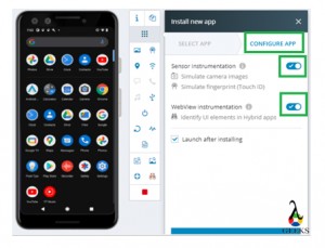
Step8: Configuring app setting

When the application installation is completed, please do the necessary configuration for app testing. To do the same, please select “CONFIGURE APP” and please make the radio button on or off as per your testing requirement.

Image8 Configure app settings
A Complete Guide for Perfecto Cloud access_Configure App Setting

Step9: To get the device ID or device attribute capability 

To start automation for mobile applications, we need to make the application and device synchronization; we need to configure device attributes.

We can get attribute details from selecting the “Capabilities” option.

Image10 Capturing screenshot
A Complete Guide for Perfecto Cloud access_Capture Screenshot

Step10: Capturing screenshot during testing 

Capturing the screenshot feature helps the tester to collect the evidence for any defect/error/issue. It enables the developer to debug and fix the problem.  

Image10 Get device attribute
A Complete Guide for Perfecto Cloud access_Get Device Attribute

Step11: Release the Cloud device

When the user completes the testing, the device needs to be released so that other users can use it for testing.  

A Complete Guide for Perfecto Cloud access
A Complete Guide for Perfecto Cloud access_Release Cloud Device

Conclusion

In this topic, We have covered how to reserve a mobile device from Perfecto Cloud and do manual testing. In the next topic, We will write about Perfecto configuration and set up for Automation. For more details on Perfecto, please refer to this link.

11 Facts On Voltage Regulator:Types,Circuits,Applications !

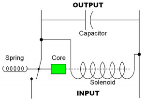
450px Simple electromechanical voltage regulator 300x207 1
  • What is a Voltage regulator
  • Types of a voltage regulator
  • Voltage regulator Circuit
  • Zener Diode as a voltage regulator
  • Difference between series regulator & shunt regulator
  • Series regulator
  • Shunt regulator
  • Regulated power supply
  • The function of the voltage regulator
  • Percentage regulation
  • Applications of a voltage regulator

Definition of voltage regulator:

A voltage regulator is a DC regulator that offers a constant DC output voltage that is fundamentally independent of applied input voltage, output load current, and temperature.”

Also, the regulator output can be changed as per the requirement. Hence, the function of a voltage regulator is two-fold 1. The output voltage can be regulated at the desired level. 2. The regulated voltage at the output can be maintained constant despite disturbances in supply voltage or change in load.

Voltage Regulator Types:

  • The Zener Diode Based Shunt Regulators
  • The Transistor Based Shunt Regulators
  • The Transistor Series Regulators
  • The Transistor Current Regulators
  • The Transistor Controlled Series Regulators
  • The Op-amp based Shunt Regulators
  • The Op-amp based Series Regulators
  • The Switching Voltage Integrated Circuit Regulators
  • The Monolithic Regulators

Voltage Regulator Circuit:

The following figure refer to the Zener diode of a regulator.

450px Simple electromechanical voltage regulator
Voltage Regulator Circuit, Image Credit – anonymous, Simple electromechanical voltage regulatorCC BY-SA 2.5

The input current, IS=VS-VZ/RS

Where VS= d.c input voltage to the regulator circuit VZ= Zener voltage

The voltage across Zener diode terminals,

VL=VZ + IZ rz

VL=VZ (Itrz is negligible)

IL=VL/RL

Input current, IS=IZ + IL or IZ= IS – IL

Zener Diode as Voltage Regulator:

Voltage stabiliser transistor IEC symbols
Zener Diode as Voltage Regulator Image Credit – I, AppaloosaVoltage stabiliser transistor, IEC symbolsCC BY-SA 3.0

In this circuit, a Zener diode is joined in reverse biased parallel with a variable voltage source supply. The Zener diode in this circuit will operate when the voltage at the reverse breakdown voltage. Then, the diode’s relatively low impedance retains the voltage.

This is a typical voltage regulation circuit with an input voltage, VIN. This voltage is regulated down to a stable output voltage, namely VOUT. The breakdown diode voltage is stable over a wide current range and maintains VOUT at relatively constant even though the relative voltage may fluctuate during this operation.

As per Ohm’s law diode current, flowing through the diode, a load is placed across the diode, and as long as the Zener diode operates in a reverse breakdown, the diode will deliver a stable voltage to the load. Zener diodes in this stage are often used as a stable regulator for more advanced circuitry.

Series Regulator Circuit:

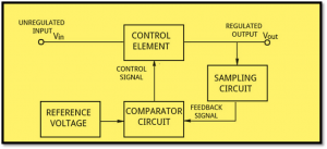
The basic block diagram of the series regulator circuit is shown below. The control element is connected in series with the load in between i/p and o/p terminal. The sampling circuit detects the variation in the output voltage. The comparator circuit will compare sample voltage with a reference one. The control element will compensate during that period and will retain a constant output. The control element conducts more when V0 reduces and conducts less when V0 increases.

DG 3
Series Voltage Regulator

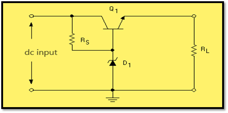
Here a simple series regulator is presented. Transistor Q is the controlling element that is in series. The Zener diode provides the reference voltage.

Voltage stabiliser OA IEC symbols
Regulator with op-amp, Image Credit – I, AppaloosaVoltage stabiliser OA, IEC symbolsCC BY-SA 3.0

Shunt Regulator Circuit:

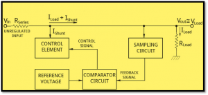
In the linear voltage regulator category, in the shunt regulator circuit, the output is monitored, and the feedback signal initiates changes in input signals to maintain the desired output. However, in series regulators, the control unit or regulating unit is in series, and in shunt regulators, the control unit is in the shunt. The basic block diagram is shown below,

DG 5
Shunt Voltage Regulator

In the case of shunt regulators, as the control element is in shunt, it conducts more to provide regulation by shunting current away from the load.

DG 6

What is Regulated Power Supply?

A regulated power supply is a stand-alone unit. It is able to supply a stable voltage to a circuit. This has to be operated within specific power supply limits. The regulated power supply output might be alternating or unidirectional but it is nearly a DC in standard operation.

The type of stabilization be limited to confirm that the output remains within absolute limits under a number of load condition.

The specification parameters are:

  • The Input Voltage parameter
  • The Output Voltage parameter
  • The Output Current parameter
  • Stability factor
  • Ripple factor
  • The Stored Energy
  • The Pulsed operations
  • The Load Regulation
  • The Line regulation
  • The Dynamic Regulation
  • The Efficiency.

Comparison between Shunt and Series Regulator

ParameterShunt Voltage  RegulatorSeries Voltage Regulator
ConnectionIt is connected in parallel with loadIt is connected in series with load
Load CurrentAt high load current, has good voltage regulation.At high load current, does not have an effective voltage regulation.
OutputConstant DC Output voltage.Varying Output voltage.
Control ElementHigh voltage low current circuitryHigh current low voltage circuitry.
SuitabilityIt is good for light loadsIt is good for heavy loads.
EfficiencyGood efficiency for low load current.Good efficiency for heavy load current.

What is the function of a Voltage Regulator?

A voltage regulator is to provide a constant DC output which is independent of the input voltage, output load current, and the temperature. It is an important component of a power supply circuitry. Its input voltage supplied from the rectifier circuit. The low capacity (500VA) regulators are in general used for domestic applications, for television, refrigerator, air-conditioner, etc. and for necessary equipment like computers. In these medical instruments, the sudden changes in voltages can affect the equipment leading to erroneous results and may get damaged ultimately.

What is the Percentage Regulation?

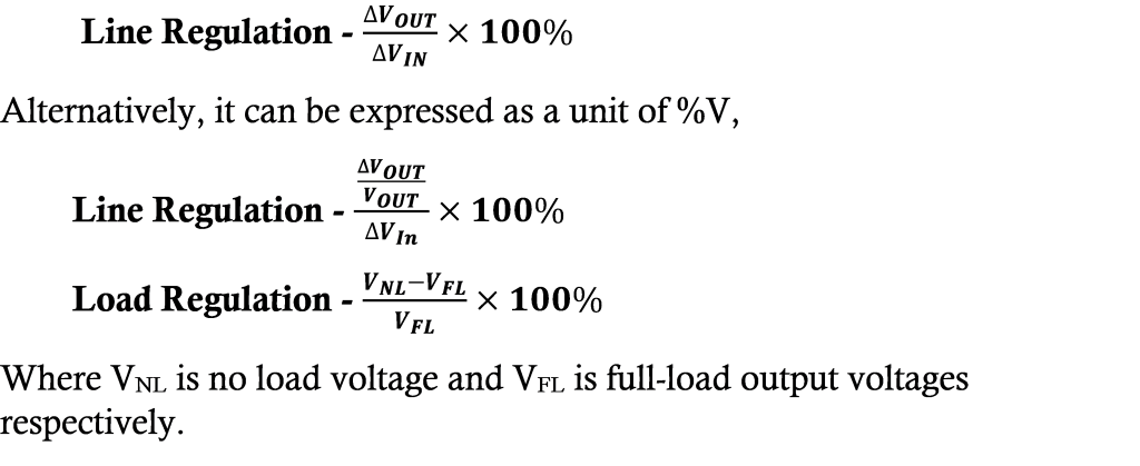
The basic performance measures for a regulator are line regulation and load regulation parameter. The line regulation is defined as the change in percentage of the output voltage for a given change in the input voltage as explains follows:

DG 7

Uses of Voltage Regulators:

  • Voltage Regulators is used in low output voltage switching power supply circuits.
  • It is used in error amplifiers design.
  • In design of the current source and  the sink circuits
  • These are used for voltage monitoring and maintenances.
  • It is used to design the Precision current limiter circuitry. It is applied in Analog and Digital Circuits for precision reference.
  • It is used in adjustable voltage or current linear circuitry etc.

33 Essential Interview Questions On Transistor(BJT, FET & MOSFET)

Most Frequently asked interview questions on transistor in the topic such as BJT, FET and MOSFET.

1.   BJT is

  1. a voltage control device
  2. a current controlled device
  3. a temperature controlled device
  4. none of these

Answer – (2)

2.   In NPN BJT electrons are energized in

  1. forward biased junction
  2. reverse biased junction
  3. bulk region
  4. both the junctions

Answer – (4)

3.   When a transistor operating at the central of the load line is declining, the current gain will change the Q-point

  1. down
  2. up
  3. nowhere
  4. of the load line

Answer – (3)

4.    The output voltage of a Common Emitter amplifier is

  1. amplify
  2. reverse
  3. 180° out of the phase with the input
  4. all of these

Answer – (1)

5.   The level of doping of emitter section of a transistor has to be

  1. More than the collector and base.
  2. Smaller than the collector and base.
  3. lesser than the base region but greater than the collector region
  4. More than base region only

Answer – (3)

6.   A BJT used in Common Emitter configured offers

  1. low input & high output impedance
  2. high input & low output impedance
  3. low input & output impedances
  4. high input & output impedances

Answer – (2)

7.   A bipolar junction transistor when used as a switch, operates in

  1. cut-off and active region
  2. active and saturation region
  3. cut-off and saturation region
  4. all of these

Answer – (3)

8.   If for CE model hie  = 1k.ohm, hfe = 50 then for common collector model hie . hfe will be

  1. 1 k.ohm,50
  2. 1k.ohm,51
  3. 1/51 k.ohm,50
  4. 1/51 k.ohm, -51

Answer -(2)

9.   The leakage current ICBO flows through

  1. base and emitter terminals
  2. emitter and collector terminals
  3. base and collector terminals
  4. emitter,base and collector terminals

Answer – (3)

10. To turning OFF an SCR, it is essential to decrease current to be less than

  1. trigger current
  2. holding current
  3. break over current
  4. none of these

Answer – (1)

11. In a BJT, the base region should be very thin to minimalize the

  1. drift current
  2. diffusion current
  3. recombination current
  4. tunneling current

Answer – (3)

12.  A transistor configuration with the lowermost current gain is

  1. common base
  2. common emitter
  3. common collector
  4. emitter follower

Answer – (4)

13.  When a transistor is acting as a switch operate in

  1. cut-off region
  2. saturation region
  3. active region
  4. both a & b

Answer – (4)

14.  The Transistor is connected in Common Base configuration has

  1. high input & low output resistance
  2. low input & high output resistance
  3. low input & low output resistance
  4. high input & high output resistance

Answer – (1)

15.  An N-channel MOSFET, the source and drain region has to be doped with

  1. n-type material
  2. p-type material
  3. source with p-type and drain with n-type material
  4. none of these

Answer – (2)

16. JFET normally works

  1. In the cut-off mode
  2. In the saturation mode
  3. In the Ohmic mode
  4. In the break down mode

Answer – (3)

17. In a p-type MOSFET in accumulation region, the band bends

  1. downwards
  2. sideways
  3. upwards
  4. none of these

Answer – (3)

18.  When the drain saturation current is >= Idss a JFET operate as

  1. The bipolar transistor
  2. The current source
  3. Simple resistor
  4. A battery

Answer – (3)

19. Strong inversion occurred in N-MOSFET for condition

  1. Φ s = Φ F
  2. Φ = 2Φ F
  3. Φ s  = 0
  4. Φ s < Φ F

Where, Φ  and Φ F   are surface and Fermi potential respectively

Answer – (2)

20. A D-MOSFET typically operate in

  1. The depletion mode only.
  2. The enhancement mode only.
  3. The both depletion & enhancement mode.
  4. The small impedance mode.

Answer – (3)

21. Ion implantation is done

  1. at lower temperature than diffusion mode
  2. at higher temperature than diffusion mode
  3. at most same temperature as diffusion mode
  4. none of these

Answer – (1)

22. The Flat band condition for an MOS capacitor is

  1. Φ s  = 0
  2. Φ s  > 0
  3. Φ s  < 0
  4. Φ s  = Φ F

Answer – (1)

23. Inversion layer in an MOS circuit is made by

  1. doping
  2. impact ionization
  3. tunneling
  4. electric field

Answer – (4)

24. Compared to Field Effect Phototransistor, Bipolar Phototransistors are

  1. more sensitive and faster
  2. more sensitive and slower
  3. less sensitive and slower
  4. less sensitive and faster

Answer – (3)

25. Consider the following statements

The threshold voltage of a MOSFET can be increased by

  • I. using thinner Gate Oxide
  • II. reducing the substrate concentration
  • III. increasing the substrate concentration of these
  1. III alone is correct
  2. I & II are correct
  3. I & III are correct
  4. II alone is correct

Answer – (2)

26. The function of the SiO2 layer in MOSFET is to provide

  1. The high input impedance
  2. The high output impedance
  3. flow of current carries within channel
  4. both a & b

Answer – (3)

27. Above pinch off voltage in a JFET the drain current

  1. decreases
  2. increases sharply
  3. remains constant
  4. both a & b

Answer – (3)

28. If V is the voltage applied to the metal with respect to p-type semiconductor in a MOS capacitor then V<0 corresponds to

  1. accumulation
  2. depletion
  3. inversion
  4. strong inversion

Answer – (1)

29. Flat-Band voltage of n-channel enhancement type MOSFET is

  1. positive
  2. negative
  3. positive or negative
  4. zero

Answer – (1)

30. Which one of the following is not a voltage controlled circuit?

  1. MOSFET
  2. IGBT
  3. BJT
  4. JFET

Answer – (3)

31. Pinch off voltage of FET depends on

  1. channel width
  2. doping concentration of channel
  3. applied voltage
  4. both of a & b

Answer – (4)

32. For design of a high speed electronic system the preferred one should be

  1. Si n-MOS
  2. Si p-MOS
  3. GaAs n-MOS
  4. GaAs p-MOS

Answer – (3)

33. What is one significant thing transistors perform?

  1. Amplify weak signals
  2. Rectify line voltage
  3. Regulate voltage
  4. Emit light

Answer – (1)

34. The base of an NPN transistor is thin and

  1. Heavily doped
  2. Lightly doped
  3. Metallic
  4. Doped by a pentavalent material

Answer – (2)

35. Maximum no electrons in the base region of an NPN transistor will not recombine for reason being

  1. Have a long lifetime
  2. Have a negative charge
  3. Must flow a long way through the base
  4. Flow out of the base

Answer – (1)

UFT Tutorial: UFT Overview (Beginner’s Guide!)

UFT Overview

After developing, the software product has to be passed through the testing phase to ensure the quality. In the testing life cycle, test automation has a brighter future as it has the ability to reduce the testing cycle and cost with expected quality check. Many tools are available for test automation, but if we consider the broader application coverage, the Unified Functional Test(UFT) tool is one of the key player.

Through out this “UFT Overview” article, we will go through the basics of testing and overview of different components which are available in UFT.

UFT Tutorial – Table of Content

UFT Overview

About Software Testing:

Testing has the importance for cross verification of the end product. Testing can be done in different phases of software development life cycle. We can perform the software testing in two ways – manually or through test automation. We will talk about test automation through out the tutorials. 

The purposes of software testing are explained below –

  • Verification of the quality of the end product..
  • Find and fix the bugs before deploying the software in production.
  • Testing can assure about the software requirement.
  • Report if there is any performance or security issues.

The classification of software testing are explained below –

  • Unit Testing – This type of testing are done in the development phase by the application developer.
  • Integration Testing – After the development, when all the components are integrated, the integration testing is required to ensure the interfaces and the different software components are working as expected.
  • System Testing – This type of testing is done before delivering the end product. The functionalities of the product are tested in this phase.
  • User Acceptance Testing – The User Acceptance Testing(UAT) is done by the business users to check the requirements before deploring the product into production. This is a blac-kbox testing.
  • Regressing Testing – Regression testing is required to verify the business-as-usual functionalities during the application enhancements.

About Automation Testing:

In todays life, time is an important criteria for the software testing process. So, there is a high demand to reduce the test execution cycle without compromising with the quality. In this particular aspect automation testing is come into the picture. Automated testing is nothing but the testing has to be done automatically without spending any human efforts. Many tools are available to perform test automation like RFT, QTP (UFT), and Selenium. But, considering the application coverage and flexibility, UFT is ruling the test automation industry. In this tutorial, we will provide an overview idea of UFT as a test automation tool.

The key features of test automation are mentioned below –

  • Automated test execution is always very fast with compare with manual testing cycle.
  • Common human errors can not be replicated in test automation.
  • It reduces the test execution cycle time which helps to reduce the entire software development life cycle as well.
  • Ensures the quality by covering more functionalities.
  • Parallel test execution can be done.

About UFT Overview:

UFT is the short form of Unified Functional Testing, which is previously known as Quick Test Professional (QTP). With the help of VB Scripting, test cases build to automate any functional testing scenario. The primary merits of UFT over other test automation tools, are specified below –

  • Test automation process is simple and easy to learn the tool in a shorter span of time.
  • Automation can be done through the recording.
  • Identification of test object is more efficient and robust.
  • It’s easily compatible with different standard test automation frameworks.
  • It has more application coverage. The famous application platforms (e.g., Web, SAP, SFDC, mobile, etc.) are compatible with UFT.
  • UFT supports web service testing(API) and XMLs.
  • It supports vbscripting which is easy to learn
  • We can easily integrate the UFT with ALM as a test management tool.
  • It has an in-build excel sheet like dataTables which helps to develop test data driven approach easily.
  • In-build reporting is available with the tool during execution.

Different important components of UFT are specified below –

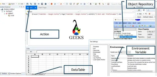
  • Action –Actions are the actual container of the test scripts i.e., we can develop the test case in a action. The application functionalities can be broken into small logical blocks/ modules using the actions.
  • Object Repository – The technical properties of test objects are stored in object repository (OR) which are used to develop the automated test cases in UFT.
  • Datatable – The another important features of UFT is datatable which is used for test data management. Based on the usage and looks, it’s comparable to Microsoft excel sheet. We can add, edit, delete data at any time from the datatable. The datatable allows us to design the data-driven automation test framework.
  • Function Library – The function library in UFT, contains the user defined functions and sub procedures. Conceptually, function is a block of codes or statements which are used to perform a specific task. To access the functions from the function libraries, first, we need to associate the library with the UFT test cases.
  • Environment Variable – UFT allows us to store configuration related test data which will be accessible through out the entire test suite in a special kind of variables. This variables are known as environment variable. Three types of environment variables are available – In built, internal user defined and external user defined environment variables. Details on environment variables are available here.
UFT Overview
UFT Overview

About Automation Test Framework: 

The automation test framework defines some standard guidelines which help to perform test automation test activities in a organized and efficient way. The purposes of automation test frameworks as specified below –

  • Use the same standards through out all the test cases.
  • Increase the speed of test automation activities such as development, execution, maintenance etc.
  • Easy to debug the failed test cases.
  • Using of predefined standards, there is better readability.
  • Reduces the test execution efforts by implementation of unattended execution.
  • Test data can be managed in a structured way by defining the proper frameworks.

In the below section, the all types of automated test frameworks are explained –

Linear Automation Framework –

This type of automation test frameworks are also known as record and play framework. The reason behind this naming convention is that the test cases are created by recording the test scenario by the UFT Recording feature. This type of test case does not contain data parameterization, reusable components etc. Here, the test cases can be created quickly with minimum skillset of tester. This test framework is popular for one time test execution but not advisable to use for long run. As it needs much more maintenance efforts if we compare with other frameworks.

Modular Driven Framework – 

The name suggest that test cases are driven by reusable modules which means that the entire test scenario is broken into small parts as modules. By clubbing the modules, we can create the test cases. The modules can be created using reusable actions or procedures with the help shared object repository. Before starting the scripting, we need to analyze the entire test scenarios and identify the small sections which can be reused again and again.

As the modules are the driver in this test framework, the test maintenance efforts are very less if we compare with linear test framework. This framework approach is very useful for any application where different test flows are available.

Data-Driven Framework –

As per the name suggest, the test cases are driven by test data in data-driven test framework. The test data can be stored in datatables, excel sheet, databases or csv files which will be fetched and used during the test execution. This framework is very useful for applications where single flow is available and based on different data criteria, different test cases are created. It minimizes the number of test cases as same test case can be executed for different set of test data. Thus, it reduces the maintenance efforts as well.

Keyword Driven Framework – 

The keyword-driven test framework is also called the table-driven testing. The first step of this framework is to develops the keys which represent the small modules such as invoke, login, enterData, clickSubmit, verify, logout, etc. Then, by specifying the keys in predefined excel or datatable along with data and operation, we can develop the test cases. In this framework, one driver script is required which reads the excels or datatable and perform the corresponding task as per the keys. This is best fitted for small projects and due to usage of reusable keys, the maintenance efforts are very less. The main disadvantage of this keyword driven framework is the complexity.

Hybrid Test Framework –

By combining two or more test frameworks which are explained above, we can define the hybrid test frameworks. This types of frameworks are mostly used for any test automation projects.

UFT Overview - Test Framework
UFT Overview – Test Framework

Conclusion:

In this article about UFT Overview, we have learned about the overview of automation testing, components of UFT, and test frameworks. Click here to understand more from the Microfocus support portal.

UFT Setup – Complete HandsOn Guide And Steps!

UFT Setup Registration to Download UFT

Through out this UFT Setup article, we will explain the step by step approach of UFT Setup, which includes download. Install, License Configuration, and ALM Connection.

The software testing now the hot topic on software development life cycle to ensure the quality of the end product. Also the marked demands the faster delivery of the product with the best quality. On this aspect, test automation plays the major role to reduce the test cycle time. In the market, different types of automation test tools are available. But, Unified Functional Testing (UFT in shorter form) is playing the key role in the market.

UFT Tutorial – Table of Content

 UFT Tutorial #2: UFT Setup

Download UFT:

  • Step1: Open the microfocus site and click on the corresponding link to download the latest UFT.
  • Step2: Enter the below details to register for the UFT Trial version.
UFT Setup - Registration to Download UFT
UFT Setup – Registration to Download UFT
  • Step3: Click on Start Free trial to download software and unzip it if required.

Install UFT

  • Step1: Uninstall the existing UFT version from the system (if any).
  • Step2: Execute the setup file with Admin privilege, which was downloaded previously.
UFT Setup - Install UFT Step2
Install UFT Step2
  • Step3: Enter the location to extract temp files and click on Next.
UFT Setup - Install UFT Step3
Install UFT Step3
  • Step4: Update window components (if required). Click OK.
UFT Setup - Install UFT Step4
Install UFT Step4
  • Step5: Click on the Next button and accept terms and condition
UFT Setup - Install UFT Step5
Install UFT Step5
  • Step6: Select required Addons to automate corresponding applications. Also, the Installation directory can be modified from here.
UFT Setup - Install UFT Step6
Install UFT Step6
  • Step7: Keep the default selection and click on the Install button and wait for the completion of the installation.
UFT Setup - Install UFT Step7
Install UFT Step7
  • Step8:  Click on the Finish button to close the setup wizard.
UFT Setup - Install UFT Step8
Install UFT Step8
  • Step9: Install Microsoft Script Debugger by executing scd10en.exe file with admin privilege. The script debugger is available in Microsoft’s official page to download.

UFT License Configuration

  • Step1: Open the UFT with admin privilege(for the first time only).
UFT Setup - UFT License Configuration Step1
UFT Setup – UFT License Configuration Step1
  • Step2: Click on the Install Licence button from the error message(if it appears).
UFT Setup - UFT License Configuration Step2
UFT Setup – UFT License Configuration Step2
  • Step3: Click on the “Concurrent License” section.
UFT Setup - UFT License Configuration Step3
UFT Setup – UFT License Configuration Step3
  • Step4: Enter the License server as “mlgccu01devat02” and click on Connect. Some time error may appear (in the error case, retry for a couple of times after restarting the server)
UFT Setup - UFT License Configuration Step4
UFT Setup – UFT License Configuration Step4
  • Step5: If connection success, click on the INSTALL button.
UFT Setup - UFT License Configuration Step5
UFT Setup – UFT License Configuration Step5
  • Step6: License server connected successfully now. Click on EXIT WIZARD and reopen the UFT tool.
UFT Setup - UFT License Configuration Step6
UFT Setup – UFT License Configuration Step6
  • Step7: After the successful installation of the license server, the below addon selection screen should appear.
UFT Setup - UFT License Configuration Step7
UFT Setup – UFT License Configuration Step7

ALM Connection

ALM is used as a script repository of UFT test cases. Also, we can manage the test execution, status reporting, defect management through the ALM. In this section, we will learn how to connect ALM from the UFT.

  • Step1: Open the UFT with admin privilege. Admin access is required to download the required DLL files to establish a connection with ALM. This is a one-time activity.
  • Step2: Select required addon and click OK to open UFT…
  • Step3: Click on the “ALM Connection” icon.
UFT Setup - ALM Connection Step3
UFT Setup – ALM Connection Step3
  • Step4: Enter ALM Server URL and user credential. Server URL – http://xxxxxxxxx/qcbin/ and click on Connect.
UFT Setup - ALM Connection Step4
UFT Setup – ALM Connection Step4

It will take a couple of minutes to download ALM components(DLLs).

  • Step5: Select the ALM projects and click on the Login button.
UFT Setup - ALM Connection Step5
UFT Setup – ALM Connection Step5

Conclusion:

In this article about UFT Setup, we have learned about how to download, install, and configure UFT for test automation. To know more details on UFT from support portal, please click here. Also, if you want to prepare for UFT Interview Questions, please click here.