Microwave Resonators: 5 Important Factors Related To It

MR 1 300x122 1

Points of Discussion: Microwave Resonators

Introduction to Microwave Resonators

Microwave resonators are one of the crucial elements in microwave communication circuit. They can create, filter out, and select frequencies in various applications, including oscillators, filters, frequency meters, and tuned oscillators.

Operations of microwave-resonators are very much like the resonators used in network-theory. We will discuss the series and parallel RLC resonant circuits at first. Then, we will find out various applications of resonators at microwave frequencies.

Know about Microwave Engineering and Its Overview. Click Here!

Series Resonator Circuit

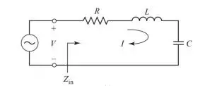
A series resonator circuit is made by arranging a resistor, an inductor, and a capacitor in series connection with a voltage source. The circuit diagram of a series RLC is given below. It is one of the type of microwave resonators.
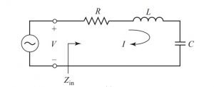
Microwave Resonators
Series Resonator Circuit, Microwave Resonators – 1

The input impedance of the circuit is given as Zin = R + jωL − j /ωC

The complex power from the resonator is given by Pin.

Pin = ½ VI* = ½ Zin | I|2 = ½ Zin | (V/Zin) |2

Or, Pin = ½ |I|2 (R + jωL − j /ωC)

The power by the resistor is: Ploss = ½ |I|2 R

The average magnetic energy stored by the inductor L is:

We = ¼ |Vc|2 C = ¼ |I|2 (1/ω2C)

Here, Vc is the voltage across the capacitor.

Now, complex power can be written as follow.

Pin = Ploss + 2 jω (Wm − We)

Also, the input impedance can be written as: Zin = 2Pin/ |I|2

Or, Zin = [Ploss + 2 jω (Wm − We)] / [½ |I|2]

In a circuit, resonance occurs when the stored average magnetic field and the electric charges are equal. That means, Wm = We. The input impedance at resonance is: Zin = Ploss / [½ |I|2] = R.
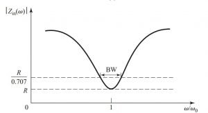
Microwave Resonators
Graph: Input impedance magnitude and frequency, Microwave Resonators – 2

R is a pure real value.

At Wm = We, the resonance frequency ω0 can be written as ω 0 = 1/ √(LC)

Another critical parameter of the resonant circuit is the Q factor or quality factor. It is defined as the ratio of the average energy stored to the energy loss per second. Mathematically,

Q = ω * Average energy change

Or Q = ω *(Wm + We) / Ploss

Q is a parameter which gives us the loss. Higher Q value implies the lower loss of the circuit. Losses in a resonator may occur due to loss in conductors, dielectric loss, or radiation loss. An externally connected network may also introduce losses to the circuit. Each of the losses contributes to the lowering of the Q factor.

The Resonator’s Q is known as Unloaded q. It is given by Q0.

The unloaded Q or Q0 can be calculated from the previous equations of Q factor and Power loss.

Q0 = ω 0 2Wm / Ploss = w0L / R = 1/ w0Rc

From the above expression, we can say that the Q decreases with the increase of R.

We will now study the behaviour of the input impedance of the resonator circuit when it is near its resonance frequency. Let w = w0 + Δω, here Δω represents a minimal amount. Now, the input impedance can be written as:

Zin = R + jωL (1 − 1/ω2LC)

Or Zin = R + jωL ((ω2 – ω02)/ω2)

Now, ω20 = 1/LC and ω2 − ω20 = (ω − ω0) (ω + ω0) = Δω (2ω − Δω)2ω Δω

Zin ~ R + j2L Δω

Zin ~ R + j2RQ0L Δω / ω0

Now, the calculation for half-power fractional bandwidth of the resonator. Now, if the frequency becomes |Zin| 2 = 2R2, the resonance receives 50% of the total delivered power.

One more condition is such that when the Band Width value is in fraction, the value of Δω/ω0 becomes half of the Band Width.

|R + jRQ0(BW)| 2 = 2R2,

or BW = 1/Q0

Know about Transmission Lines and waveguides. Click Here!

Parallel Resonant Circuit

A parallel resonator circuit is made by arranging a resistor, an inductor, and a capacitor in parallel with a voltage source. The circuit diagram of a parallel RLC is given below. It is one of the type of microwave resonators.
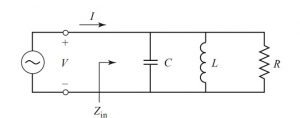
Microwave Resonators
Circuit: Parallel Resonator Circuit, Microwave Resonators – 3

Zin gives the input impedance of the circuit.

Zin = [1/R + 1/jωL + jωC] −1

The complex power delivered from resonator is given as Pin.

Ploss = ½ VI* = ½ Zin | I|2 = ½ Zin | V|2 / Zin*

Or Pin = ½ |V|2 (1/R + j/wL – jωC)

The power from resistor R is Ploss.

Ploss = ½ |V|2 / R

Now, the Capacitor also stores the energy, it is given by –

We = ¼ |V|2C

The inductor also stores the magnetic energy, it is given by –

Wm = ¼ |IL|2 L = ¼ |V|2 (1/ ω2L)
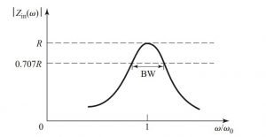
Microwave Resonators
Graph: Input impedance magnitude with frequency, Microwave Resonators – 4

IL is the current through the inductor. Now, the complex power can be written as: Pin = Ploss + + 2 jω (Wm − We)

The input impedance can also be written as: Zin = 2Pin/ |I|2 = (Ploss + 2 jω (Wm − We))/ ½ |I|2

In the series circuit, the resonance occurs at Wm = We. Then the input impedance at resonance is Zin = Ploss / ½ |I|2 = R

And the resonant frequency at Wm = We can be written as w0 = 1 / √ (LC)

It is same as the value of series resistance. Resonance for the parallel RLC circuit is known as an antiresonance.

The concept of unloaded Q, as discussed early, is also applicable here. The unloaded Q for the parallel RLC circuit is represented as Q0 = ω02Wm/ Ploss.

Or Q0 = R /ω0L = ω0RC

Now, at antiresonance, “We = Wm”, and the value of the Q factor decreases with the decrease in R’s value.

Again, for input impedance near resonance frequency consider ω = ω0 +Δω. Here, Δω is assumed as a small value. The input impedance is again rewritten as Zin.

Zin = [ 1/R + (1 – Δω / ω0) / jω0L + jω0C + jΔωC] -1

Or Zin = [ 1/R + j Δω / ω2L + jΔωC] – 1

Or Zin = [ 1/R + 2jΔωC]-1

Or Zin = R / (1 + 2jQ0Δω/ω0)

Since ω2 = 1/LC and R = infinite.

Zin = 1 / (j2C (ω – ω0))

The half-power bandwidth edges occur at frequencies (Δω / ω0 = BW/2) such that, |Zin|2 = R2/ 2

Band Width = 1 / Q0.

Transmission Line Resonators

Almost always, the perfect lumped components can not deal in the range of microwave frequencies. That is why distributed elements are used at microwave frequency ranges. Let us discuss various parts of transmission lines. We will also take into consideration of the loss of transmission lines as we have to calculate the resonators’ Q value.

For Detail Analysis of Transmission Lines… Click Here!

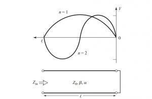
Short circuited λ/2 Line

Let us take a transmission line which suffers loss and also it is short-circuited at one of its terminal.
Microwave Resonators
Voltage Distribution and short circuited diagram of Lossy transmission line, Microwave Resonators – 5

Let us assume the transmission line has a characteristic impedance of Z0, the propagation constant of β and attenuation constant is α.

We know that, at resonance, the resonant frequency is ω = ω0. The length of the line ‘l’ is λ/2.

The input impedance can be written as Zin = Z0 tanh (α + jβ)l

Simplifying the tangential hyperbolic function, we get Zin.

Zin = Z0 (tanh αl + j tan βl) / (1 + j tan βl tanh αl).

For a lossless line, we know that Zin = jZ0 tan βl if α = 0.

As discussed earlier, we will consider the loss. That I why, we will take,

αl << 1 and tanh αl = αl.

For a TEM line,

βl = ωl/ vp = ω0l/ vp + Δωl/ vp

vp is an important parameter which represents the transmission line’s phase velocity. L = λ/2 = πvp0 for ω = ω0, we can write,

βl = π + Δωπ/ ω0

Then, tan βl = tan (π + ωπ/ ω0) = tan (ωπ/ ω0) = ωπ/ ω0

Finally, Zin = R + 2 jLω

At last, the value of resistance comes as: R = Z0αl

The value of inductance comes as : L = Z0π/ 2ω0

And, the value of Capacitance comes as : C = 1/ ω20L

The unloaded Q of this resonator is, Q0 = ω0L/ R = π/ 2αl = β/ 2α

Solved mathematical Example of Microwave Resonators

1. A λ/2 resonator is made up of copper coaxial line. Its inner radius is 1 mm, and the outer radius is 4mm. The value of the resonant frequency is given as 5 GHz. Comment on the calculated Q value of two coaxial line among which one is filled with air another filled with Teflon.

Solution:

a = 0.001, b = 0.004, η = 377 ohm

We know that the conductivity of the copper is 5.81 x 10⁷ S/m.

Thus, the surface resistivity at 5GHz = Rs.

Rs = root (ωµ0/ 2σ)

Or Rs = 1.84 x 10⁻² ohm

Air filled attenuation,

αc = Rs /2η ln b/a {1/ a + 1/ b}

Or αc = 0.22 Np/m.

For Teflon,

Epr = 2.08 and tan δ = 0.0004

αc = 0.032 Np/m.

There is no dielectric los due to air filled, But for Teflon-filled,

αd = k0 √epr/2 * tan δ

αd = 0.030 Np/m

So, Qair = 104.7 / 2 * 0.022 = 2380

Qtefflon = 104.7 * root(2.008) / 2 * 0.062 = 1218
Transmission Lines & Waveguides: 7 Important Explanations

TL 1 300x191 1

Points of Discussion : Transmission lines and Waveguides

Detail analysis of Transmission Lines! Check out here!

Introductions to Transmission Lines(TL) & Waveguide(WG)

The invention and development of transmission lines and other waveguides for the low-loss transmission of power at high frequency are among the earliest milestones in the history of microwave engineering. Previously Radio Frequency and related studies were revolved around the different types of transmission medium. It has advantages for controlling high power. But on the other hand, it is inefficient in controlling at lower values of frequencies.

Two wires lines cost less, but they have no shielding. There are coaxial cables that are shielded, but it is difficult to fabricate the complicated microwave components. Advantage of Planar line is that it has various versions. Slot lines, co planar lines, micro-strip lines are some of its forms.  These types of transmission lines are compact, economical, and easily integrable with active circuit devices.

Parameters like constant of propagation, characteristic impedance, attenuation constants consider how a transmission line will behave. In this article, we will learn about the various types of them. Almost all transmission lines (who have multiple conductors) are capable of supporting the transverse electromagnetic waves. The longitudinal field components are unavailable for them. This particular property characterizes the TEM lines and wave-guides. They have a unique voltage, current, and characteristic impedance value. Waveguides, having a single conductor, may support TE (transverse electric) or TM (transverse magnetic), or both. Unlike Now, Transverse Electric and Transverse Magnetic modes have their respective longitudinal field components. They are represented by that property.  

Know about 7+ Applications of Microwave Engineering and Overview. Click Here!

Types of waveguides

Though there are several types of waveguides, some of the most popular are listed below.

Types of Transmission Lines

Some of the types of transmission lines are listed below.

  • Stripline
  • Microstrip line
  • Coaxial line

Parallel Plate Waveguide

Parallel plate waveguide is one of the popular types of waveguide, which are capable of controlling both Transverse Electric and Transverse magnetic modes. One of the reason behind the popularity of parallel plate waveguide is that they have applications in model making for the greater-order modes in lines.

Transmission lines and Waveguides
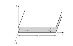
Geometric Representation of Parallel Plates Waveguides, Transmission lines and Waveguides – 1

The above image (Transmission lines and waveguides) shows the geometry of the parallel plate waveguide. Here, the strip width is W and considered more significant than the separation of d. That is how fringing field and any x variables can be cancelled. The gap between two plates is filled up by a material of permittivity ε and permeability of μ.

TEM Modes

The solution of the TEM Modes is calculated with the help of solution of the Laplace’s equation. The equation is calculated considering the factor for the electrostatic voltage which lies in between the conductor plates.

TL 4
Equation, Transmission lines and Waveguides – 2

Solving, the equation, the transverse electric field comes as:

e (x,y) = ∇t ϕ (x,y) = – y^ Vo / d.

Then, the total electric field is: E (x, y, z) = h(x, y) e– jkz = y^ (Vo / d) * e-jkz

k represents the propagation constant. It is given as: k = w √ (μ * ε)

The magnetic fields’ equation comes as:

EQ1

Here, η refers to the intrinsic impedance of the medium which lies in between the conductor plates of parallel plate waveguides. It is given as: η = √ (μ / ε)

TM Modes

Transverse magnetic or TM modes can be characterized by Hz = 0 and a finite electric field value.

(∂2 / ∂y2 + k2c) ez (x, y) = 0

Here kc is the cut-off wavenumber and given by kc = √ (k2 − β2)

After the solution of the equation, the Electric filed EX comes as:

Ez (x, y, z) = An sin (n * π * y / d) * e– jβz

The transverse field components can be written as:

Hx = (jw ε / kc) An cos (nπy / d)  e– jβz

Ey = (-jB/ kc) An cos (nπy / d) e– jβz

Ex = Hy = 0.

The cut off frequency of TM mode can be written as:

fc= kc / (2π * √ (με)) = n / (2d * √(με))

The wave impedance comes as ZTM = β / ωε

The phase velocity: vp = ω / β

The guide wavelength: λg = 2π / β

TE Modes

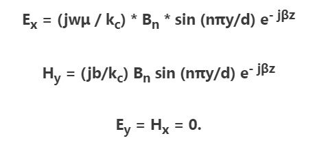
Hz (x,y) = Bn cos (nπy / d) e– jβz

Equations of the transverse fields are listed below.

EQ 2

The propagation constant β = √ (k2 – (nπ/d )2)

The cutoff frequency: fc = n / (2d √ (με))

The impedance of the TM mode: ZTE = Ex / Hy = kn/ β = ωμ/ β

Rectangular waveguide

The rectangular waveguide is one of the primary types of waveguide used to transmit microwave signals, and still, they have been used.

With miniaturization development, the waveguide has been replaced by planar transmission lines such as strip lines and microstrip lines. Applications which uses highly rated power, which uses millimeter wave technologies, some specific satellite technologies still use the waveguides.

As the rectangular waveguide has not more than two conductors, it is only capable of Transverse Magnetic and Transverse Electric Modes.

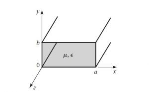
TL 2
Geometry of Rectangular Waveguide, Transmission lines and Waveguides – 3

TE Modes

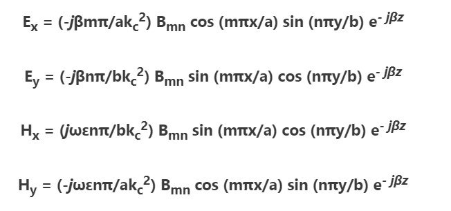
The solution for Hz comes as: Hz (x, y, z) = Amn cos (mπx/a) cos (nπy/b) e– jβz

Amn is a constant.

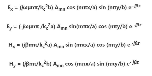
The field components of the TEmn modes are listed below:

EQ3

The propagation constant is,

EQ4
EQ5

TM Modes

The solution for Ez comes as: Ez (x, y, z) = Bmn sin (mπx/a) sin (nπy/b) e– jβz

Bmn is constant.

The field component of TM mode are calculated as below.

EQ6

Propagation constant :

EQ7

The wave impedance: ZTM = Ex / Hy = -Ey / Hx = bη * η / k

Circular Waveguide

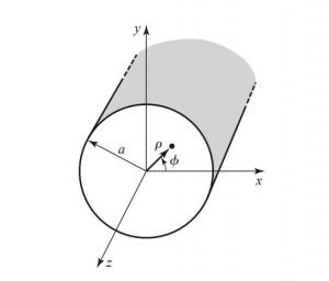
The circular waveguide is a muffled, round pipe structure. It supports both the TE and TM modes. The below image represents the geometrical description of a circular waveguide. It has an inner radius ‘a,’ and it is employed in cylindrical coordinates.

TL 3
Geometry of Circular Waveguide, Transmission lines and Waveguides – 4

Eρ = (− j/ k2c) [ β ∂Ez/ ∂ρ + (ωµ/ρ) ∂ Hz/ ∂φ]

Eϕ = (− j/ k2c) [ β ∂Ez/ ∂ρ – (ωµ/ρ) ∂ Hz/ ∂φ]

Hρ = (j /k2c) [(ωe/ ρ) ∂Ez /∂φ − β ∂ Hz/ ∂ρ]

Hϕ = (-j /k2c) [(ωe/ ρ) ∂Ez /∂φ + β ∂ Hz/ ∂ρ]

TE Modes

The wave equation is:

2Hz + k2Hz = 0.

k: ω√µe

The propagation constant: Bmn = √ (k2 – kc2)

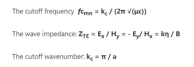
Cutoff frequency: fcnm = kc / (2π * √ (με))

The transverse field components are:

Ep = (− jωµn /k2cρ) * (A cos nφ − B sin nφ) Jn (kcρ) e− jβz

EQ8

Hφ = (− jβn/k2cρ) (A cos nφ − B sin nφ) Jn (kcρ) e− jβz

The wave impedance is:

ZTE = Ep / Hϕ = – Eϕ / Hp = ηk / β

TM Modes

To determine the necessary equations for the circular waveguide operating in Transverse magnetic modes, the wave equation is solved and the value of Ez is calculated. The equation is solved in cylindrical coordinates.

[∂2 /∂ρ2 + (1/ρ) ∂/ ∂ρ + (1 /ρ2) ∂2/ ∂φ2 + k2c] ez = 0,

TMnm Mode’s Propagation Constant ->

βnm = √ (k2 – kc2) = √ (k2 − (pnm/a)2)

Cutoff frequency: fcnm = kc / (2π√µε) = pnm / (2πa √µε)

The transverse fields are:

Eρ = (− jβ/ kc) (A sin nφ + B cos nφ) Jn/ (kcρ) e− jβz

Eφ = (− jβn /k2cρ) (A cos nφ − B sin nφ) Jn (kcρ) e− jβz

Hρ = (jωen /k2 cρ) (A cos nφ − B sin nφ) Jn (kcρ) e− jβz

Hφ = (− jωe/ kc) (A sin nφ + B cos nφ) Jn` (kcρ) e− jβz

The wave impedance is ZTM = Ep / Hφ = – Eϕ/Hp = ηβ/k

Stripline

One of the examples of planar type transmission line is Stripline. It is advantageous for incorporation inside microwave circuits. Stripline can be of two types – Asymmetric Stripline and Inhomogeneous stripline. As stripline has two conductors, thus it supports the TEM mode. The geometrical representation is depicted in the below figure.

Microwave Engineering: 5 Important Factors Related To It

442px Radar hatzerim 1 1

Points of Discussion

Introduction to Microwave Engineering

The microwave frequency range is typically 100 Mega Hertz to 1000 Giga Hertz. The range covers not only the microwave domain but also the radio frequency domain. Typical microwave domain has a frequency range of 3 MHz to 300 GHz. The corresponded electrical wavelength lies between 10 cm to 1mm. Signals having millimetre wavelengths are frequently referred to as millimetre waves. Because of the high-frequency range, typical circuit theory problems cannot solve the microwave engineering problems.

Microwave components generally act as distributed elements. The phenomena occur when the current and voltage phase varies. At lower frequencies, the wavelength gets larger. That is why there are insignificant phase changes across the dimension of the device.

Maxwell’s Theorems are one of the most used theorems in this domain.

Microwave Engineering

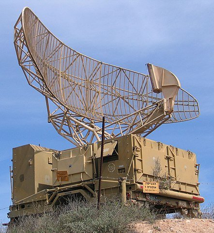
Aircraft Detector Radars,

Image Credit: BukvoedRadar-hatzerim-1-1CC BY-SA 3.0

A brief history of Microwave Engineering

Microwave engineering is one of the young and prosperous fields of engineering. The development started almost 50 years ago.The progress in this digital era in various fields is helping the microwave and RF domain to be live.

In the year 1873, James Clerk Maxwell came up with the fundamentals of Electromagnetic Theory. In the United States, a unique laboratory named as – Radiation Laboratory, was set up at the Massachusetts Institute of Technology to study, research and develop the Radar Theory. Various renowned scientists including – H. A. Bethe, R. H. Dicke, I. I. Rabi, J. S. Schwinger and several prominent scientists were there for the development in the field of RF and Microwave at that time.

Communication technologies using microwave systems started developing soon after the invention of Radar. The wide bandwidths, line-of-sight propagation of microwave technologies have proved to be necessary for both terrestrial and satellite communications. Nowadays the researches are going on the development of economic miniaturized microwave components.

Microwave Engineering
Commercial Marine Radar Antenna, Image Credit: Amada44Rotating marine radar – rotating waveguide antennaCC BY-SA 3.0

Properties of Microwaves

Microwave Engineering deals with microwave signals. Let’s analyse some of the characteristics of microwave domain. 

  1. Microwave signals have shorter wavelengths.
  2. The ionosphere cannot reflect the microwave.
  3. Microwave signals get reflected by the conducting surfaces.
  4. Microwave signals get attenuated easily within shorter distances.
  5. A thin layer of cable is enough for transmission of microwave signals.

Know about transmission lines. Click Here!

Advantages and Disadvantages of Microwave Engineering

Microwave engineering comes up with both its advantages and disadvantages. They are discussed in the later sections.

Advantages of Microwave Engineering

Microwaves have several advantages over any other domains. Let us discuss some of them.

  1. Microwave has a broader bandwidth. Thus, more data can be transmitted. For this advantage, microwave signals are used in point-to-point communications.
  2. Microwave antennas have higher gain.
  3. Size of the antenna gets reduced as the frequencies are higher and the wavelength is shorter.
  4. As microwave lie in HF to VHF, very small amount of power is consumed.
  5. Microwave signals allow having an effective reflection area for the radar systems.
  6. Line of sight propagation helps to reduce the effect of fading.

Disadvantages of Microwaves

Microwave engineering has some limitations also. Let us discuss some of them.

  1. Microwave resources are significantly costlier. Also, installation charges are high for several types of equipment.
  2. Microwave devices and systems are significant and occupy more space. However, researches are on for less space consumed devices.
  3. Microwave systems some time suffers electromagnetic interference.
  4. Inefficiency due to electric power may cause.

Applications of Microwave Engineering

High frequencies and shorter wavelengths of microwave systems create difficulties in circuit analysis. But these unique characteristics provide opportunities for the application of the microwave system. The below-mentioned considerations could be useful for practices.

  • The antenna has a property that the antenna’s gain is proportionally related to the size of the antenna. Now, for higher operational frequency, antenna gain is comparatively larger for a given physical antenna size. It also has significant consequences when implementing a microwave system.
  • More bandwidth (which is again directly related to the data rate) is gained at higher frequencies. 1% BW of 500 Mega Hertz means 5 Mega Hertz. It can give data rate around 5 Megabyte Per Second.
  • Microwave has the property of line of sight, and the ionosphere cannot reflect them.
  • One of the property of microwave signals, coupled with a gain of antennas, makes it unique and preferable.
  • Different types of resonances like molecular, atomic and nuclear happen at microwave frequency ranges. This opens up the field for several applications in basic science, remote sensing, medical science etc.
  1. The primary application of RF and Microwaves in today’s world is in wireless technologies. Technologies like – wireless communications, wireless networking, wireless security systems, radar systems, medical engineering, and remote sensing.
    • Modern day’s telephony system is evolved with the concept of cellular frequency reuse, proposed in 1947 at Bell labs. But it was practically implemented in the year 1970. In the mean-time, the demand for wireless communication increased, and miniaturization of devices was developed. Later, various communications like – 2G, 2.5G, 3G, 3.5G, 3.75G, 4G were developed using the microwave system.
  2. Satellite communications are also dependent on RF and microwave technologies. Satellites have been developed for providing cellular data, videos, data connections for the whole world. Small satellite systems like GPS and DBS has been doing great.
  3. Wireless local networks or WLANs connects computers within a short distance and provides high-speed networking. It is also an application of microwaves. Demand for WLANs are increasing day by day and will have high demands in future too.
  4. Another application of microwaves is ultra-wideband radio. Here the broadcast signal takes a vast frequency band but has a low power level. It is a precaution for avoiding interference with other systems.
  5. Radar & Military Applications: Radar systems have several applications in Defence and Militant fields, also in  profitable and research based fields. Radar is typically used to detect and mark any foreign objects inside the user’s territory in air and ground. It is also used in missile guidance and fire controls.
  6. In the commercial fields, radar systems are used in ATC (air traffic control), motion detection (like- opening and closing of the door, security alarms), vehicle collision avoidance, measurement of the distance from a point.
  7. Microwave radiometry is another application.
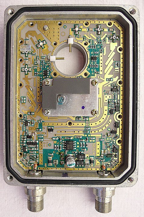
477px LNB dissassembled 1

Microstrip circuit for Satellite Television

Image Credit:SatmapLNB dissassembled, marked as public domain, more details on Wikimedia Commons

Frequently asked questions on Microwave Engineering

1. What is the frequency range for RF and microwaves?

  • Answer: RF ranges from 30 MHz to 300 MHz, and Microwaves ranges from 300 MHz to 300 GHz.

2. What are the frequency bands of microwaves?

  • Answer: There are 13 different frequency bands in the microwave range. The below list illustrates them.
Band NameRange of frequencyRange of Wavelength
L Band1 Giga Hertz – 2 Giga Hertz15 cm to 30 cm
D Band110 Giga Hertz– 170 Giga Hertz1.8 mm to 2.7 mm
Ku Band12 Giga Hertz – 18 Giga Hertz16.7 mm to 25 mm
K Band18 Giga Hertz – 26.5 Giga Hertz11.3 mm to 16.7 mm
S-Band2 Giga Hertz – 4 Giga Hertz7.5 cm to 15 cm
Ka-Band26.5 Giga Hertz – 40 Giga Hertz5 mm to 11.3 mm
Q Band33 Giga Hertz – 50 Giga Hertz6 mm to 9 mm
C Band4 Giga Hertz – 8 Giga Hertz3.75 cm to 7.5 cm
U Band40 Giga Hertz – 60 Giga Hertz5 mm to 7.5 mm
V Band50 Giga Hertz – 75 Giga Hertz4 mm to 6 mm
W Band75 Giga Hertz – 110 Giga Hertz2.7mm to 4.0 mm
X Band8 Giga Hertz – 12 Giga Hertz25 cm to 37.5 cm
F Band90 Giga Hertz – 110 Giga Hertz2.1 mm to 3.3 mm

3. Mention some disadvantages of microwaves.

  • Answer: Microwave engineering has some limitations also. Let us discuss some of them.
  1. Microwave resources are significantly costlier. Also, installation charges are high for several types of equipment.
  2. Microwave devices and systems are significant and occupy more space. However, researches are on for less space consumed devices.
  3. Microwave systems some time suffers electromagnetic interference.
  4. Inefficiency due to electric power may cause.

Cover Image By: WINDOWSCUSTOMIZATION

9 Important Solutions On Circuit Theory

MATH1 300x157 1

[Specially picked questions for GATE, JEE, NEET]

In the Circuit theory series, we have come across some fundamental yet essential rules, formulas, and methods. Let us find out some applications of them and understand them more clearly. The problems will be mainly on – KCL, KVL, Thevenin’s theorem, Norton’s theorem, Superposition theorem, Maximum Power Transfer Theorem.

Helping Hands for problem Solving on Circuit Theory:

  1. Kirchhoff’s Laws: KCL, KVL
  2. Pure AC Circuits
  3. Thevenin’s Theorem
  4. Norton’s Theorem
  5. Superposition Theorem
  6. Maximum Power Transfer Theorem
  7. Millman’s Theorem
  8. Star & Delta Connection

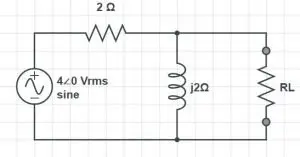
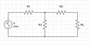
Circuit Theory: 1. Find out the maximum power which can be transferred to the load RL for the below-given circuit. Apply required theorems of Circuit Theory.

Circuit Theory
Circuit Theory Problems, Image – 1
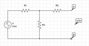
  • Solution: Remove the load resistor from the circuitry and voltage source to find out Equivalent Resistance.

So, the resistance or the impedance (AC Circuit) of the circuit through the open terminal:

ZTH = 2 || j2 = (2 x j2) / (2 +j2) = j2 / (1 +j)

Or, ZTH = 2 ∠90o / √2 ∠45o

Or, ZTH = √2 ∠45o

Now, we will calculate the current through the j2 ohms resistor.

I = 4 ∠0o / (2 +j2)

Or, I = 2 / (1+j) = √2 ∠ – 45o

The Thevenin’s equivalent voltage comes as VTH = I * j2.

Or, VTH = 2√2 ∠45o V

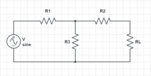
Circuit Theory
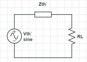
Circuit Theory Problems, Image – 2

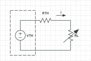
Now we can redraw the circuit in Thevenin’s equivalent circuit.

Now, from power transfer theorem, RL = | ZTH| = √2 ohm for full power.

Now, The current through the load IL = VTH / (RTH + RL)

Or, IL = 2√2 ∠45o / (√2 + √2 ∠45o)

OR, IL = 2 ∠45o / (1 + 1∠45o)

OR, IL = 2 ∠45o / [ 1 + (1 + √2) + (j / √2)]

OR, IL = 1.08 ∠22.4o A

|IL| = 1.08 So, the maximum power is: |IL2| RL = (1.08 x 1.08) x √2 = 1.65 W.

Kirchhoff’s Laws: KCL, KVL

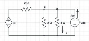
Circuit Theory: 2. Find out Norton’s equivalent resistance at terminal AB, for the below-given circuit.

Circuit Theory
Circuit Theory Problems, Image – 3
  • Solution: At first, we will apply a voltage source at the open circuit at the AB terminal. We name it VDC and assume IDC flows from it.

Now, we apply Kirchhoff’s Current Law to do nodal analysis at node a. We can write,

Circuit Theory
Circuit Theory Problems, Image – 4

(Vdc – 4I) / 2 + (Vdc / 2) + (Vdc / 4) = Idc

Here, I = Vdc / 4

Or, 4I = Vdc

Again, (Vdc – Vdc) / 2 + Vdc / 2 + Vdc / 4 = Idc

Or, 3Vdc / 4 = Idc

And, Vdc / Idc = RN

Or, RN = 4/3 = 1.33 ohm.

So, the Norton’s Equivalent Resistance is 1.33 ohms.

Circuit Theory: 3. Find out the value of R1 in Delta equivalent circuit of the given star connected network.

Circuit Theory
Circuit Theory Problems, Image – 5
  • Solution: This problem can be solved easily, using the star’s conversion formula to delta connection.
Circuit Theory
Circuit Theory Problems, Image – 6

Let us assume, that Ra = 5 ohms, Rb = 7.5 ohms, and Rc = 3 ohms.

Now, applying the formula,

R1 = Ra + Rc + (Ra * Rc / Rb)

Or, R1 = 5 + 3 + (5 x 3) / 7.5

Or, R1 = 5 + 3 + 2 = 10 ohms.

So, the R1 Delta Equivalent resistance is: 10 ohms.

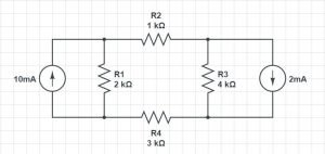
Circuit Theory: 4. Find out the current flowing through the R2 resistor for the circuit given below.

Circuit Theory
Circuit Theory Problems, Image – 7

Let us assume ‘I’ Ampere current flows through the R2 (1 kilo-ohm resistor). We can say current through 2-kilo ohm resistance will be (10 – I) Ampere (As current from 10 A source will be 10 A). Similarly, current from 2 A quotation will be 2 A and thus current through 4-kilo ohm resistance will be (I – 2) Ampere.

Now, we apply Kirchhoff’s voltage law in the loop. We can write

Circuit Theory
Circuit Theory Problems, Image – 8

I x 1 + (I – 2) x 4 + 3 x I – 2 x (10 – I) = 0

Or, 10I – 8 – 20 = 0

Or, I = 28/10

Or, I = 2.8 mA

So, the current through the R2 resistor is 2.8 mA.

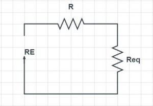
Circuit Theory: 5. If the equivalent resistance for the infinite parallel ladder given in the below image is Req, calculate Req / R. Also find the value of Req when R = 1 ohm.

Circuit Theory
Circuit Theory Problems, Image – 9
  • Solution: To solve the problem, we must know the equivalent resistance of the infinite parallel ladder. It is given by RE = R x (1 + √5)/2.

So, we can replace the circuit in the following one.

Circuit Theory
Circuit Theory Problems, Image – 10

The equivalent resistance comes here: Req = R + RE = R + 1.618R

Or, Req / R = 2.618

And when R = 1 ohm, Req = 2.618 x 1 = 2.618 ohm.

Circuit Theory: 6. A source voltage supplies voltage, Vs(t) = V Cos100πt. The source has an internal resistance of (4+j3) ohm. Find out the resistance of a purely resistive load, for transferring maximum power.

  • Solution: We know that the power transmitted for a purely resistive circuit is the average power transferred.

So, RL = √ (Rs2 + Xs2)

Or, RL = √ (42 + 32)

Or, RL = 5 ohm.

So, the load will be of 5 ohms.

Circuit Theory: 7.  Find out the Thevenin’s equivalent impedance between node 1 and 2 for the given circuit.

Circuit Theory
Circuit Theory Problems, Image – 11
  • Solution: To find the Thevenin’s equivalent impedance, we need to connect a voltage source of 1 volt in the place of node 1 and 2. Then we will calculate the current value.

So, ZTH = 1 / ITH

ZTH is the desired resistance we have to find. ITH is the current flowing due to the voltage source.

Now applying Kirchhoff’s Current law at node B,

iAB + 99ib – ITH =0

Or, iAB + 99ib = ITH ——- (i)

Applying KCL at node A,

ib – iA – iAB = 0

or, ib = iA + iAB ——- (ii)

Circuit Theory
Circuit Theory Problems, Image – 12

From equation (i) and (ii) we can write,

ib – iA + 99ib = ITH

Or, 100ib – iA = ITH ——- (iii)

Now, we apply Kirchhoff’s Voltage law at the outer loop,

10 x 103ib = 1

Or, ib = 10-4 A.

And also,

10 x 103ib = – 100iA

Or, iA = – 100iA

From equation (iii), we can write,

100iA + 100ib = ITH

Or, ITH = 200ib

Or, ITH = 200 x 10-4 = 0.02

So, ZTH = 1 / ITH = 1 / 0.02 = 50 ohms.

S, the impedance in-between node 1 and 2 is 50 ohms.

Circuit Theory: 8. A complex circuit is given below. Let us assume that both the voltage source of the circuit is in phase with each other. Now, the circuit is divided virtually in two-part A and B by the dotted lines. Calculate R’s value in this circuit for which maximum power is transferred from Part A to Part B.

Circuit Theory
Circuit Theory Problems, Image – 13
  • Solution: The problem can be solved in a few steps.

First, we find the current ‘i’ through R.

Or, i = (7 / (2 – R) A

Next, current through the 3V source,

i1 = i – (3 / -j)

Or, i1 = i – 3j

Then, we calculate the power transferred from Circuit B to A.

P = i2R + i1 x 3

Or, P = [7 / (2 – R)]2 x R + [7 / (2 – R)] x 3 —- (i)

Now, condition for transferring the maximum power is, dP / dR = 0.

So, differentiating equation (i) with respect to R, we can write:

[7 / (2 – R)]2 + 98R/ (2 + R)2 – 21/ (2 + R)2 = 0

Or, 49 x (2 + R) – 98R – 21 x (2 + R)2 = 0

Or, 98 + 42 = 49R + 21R

Or, R = 56 / 70 = 0.8 ohm

So, the R value for maximum power transfer from A to B is 0.8 ohm.

Check: Maximum Power Transfer Theorem

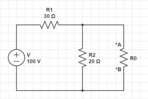
Circuit Theory: 9. Find out the value of the resistance for maximum power transferring. Also, find out the maximum delivered power.

Circuit Theory
Circuit Theory Problems, Image – 14
  • Solution: At the first step, remove the load and calculate the Thevenin’s Resistance. 

VTH = V * R2 / (R1 + R2)

Or, VTH = 100 * 20 / (20 +30)

Or, VTH = 4 V

The resistors are parallelly connected.

So, RTH = R1 || R2

Or, RTH = 20 || 30

Or, RTH = 20 * 30 / (20 + 30)

Or, RTH = 12 Ohms

Now the circuit is redrawn using the equivalent values. For maximum power transfer, RL = RTH = 12 ohms.

Maximum power PMAX = VTH2 / 4 RTH.

Or, PMAX = 1002 / (4 × 12)

Or, PMAX = 10000 / 48

Or, PMAX = 208.33 Watts

So, the maximum delivered power was 208.33 watts.

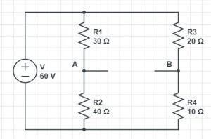
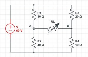
Circuit Theory: 10. Calculate the load for maximum power transferring. Find out the transferred power also.

Circuit Theory
Circuit Theory Problems, Image – 15
  • Solution:

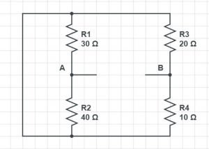
At the first step, remove the load, and calculate the Thevenin’s voltage now.

Circuit Theory
Circuit Theory Problems, Image – 16

So, VAB = VA – VB

VA comes as: VA = V * R2 / (R1 + R2)

Or, VA = 60 * 40 / (30 + 40)

Or, VA = 34.28 v

VB comes as:

VB = V * R4 / (R3 + R4)

Or, VB = 60 * 10 / (10 + 20)

Or, VB = 20 v

So, VAB = VA – VB

Or, VAB = 34.28 – 20 = 14.28 v

In the next step, calculation of resistance. As the rule says, remove the voltage and short circuit the connection.

Circuit Theory
Circuit Theory Problems, Image – 17

RTH = RAB = [{R1R2 / (R1 + R2)} + {R3R4 / (R3 + R4)}]

OR, RTH = [{30 × 40 / (30 + 40)} + {20 × 10 / (20 + 10)}]

OR, RTH = 23.809 ohms

Circuit Theory
Circuit Theory Problems, Image – 18

Now, draw the connection again with the calculated values. For maximum power transfer, RL = RTH = 23.809 ohms.

The load value will be = 23.809 ohms.

Maximum power is PMAX = VTH2 / 4 RTH.

Or, PMAX = 14.282 / (4 × 23.809)

Or, PMAX = 203.9184 / 95.236

Or, PMAX = 2.14 Watts

So, the maximum delivered power was 2.14 watts.

Star Delta Connection: 5 Important Factors Related To It

Star Delta 3

Image Credit – Pravin MishraMilky Way Galaxy As Seen From Amphulaptsa Base CampCC BY-SA 4.0

Points of Discussion

Star delta connection | Star delta transformation

Introduction to Star Connection and Delta Connection

Star and delta connections are the two very well-known methods for establishing a three-phase system. They are an essential and widely used system. This article will discuss the basics of both star and delta connections and relations between phase and link voltage and current within the system. We will also find out the significant differences between star and delta connection.

Star Connection

Star connection is the method where the similar types of terminals (all three windings) are connected to a single point, known as star point or neutral point. There are also line conductors, which are the free three terminals. The designing of wires at the external circuits makes it a three phase, three wire circuit and makes the star connection. There may be another wire named a neutral wire that makes the system a three phase, four-wire system.

Star Connection,
Star Connection, Image By – Xyzzy_n, Wye-delta-2CC BY-SA 3.0

What is meant by Thevenin’s theorem? Click Here!

The relation between Phase Voltage and Link Voltage of Star Connection

AC star connection.svg
Star Connection, Image Credit – Me (Intgr), AC star connection, marked as public domain, more details on Wikimedia Commons

The system is considered as a balanced system. For a balanced-systems, an equal amount of current will pass through all 3-phase. That is why, R, Y, B has the same value of current. Now it has consequences. This uniform distribution of current makes the magnitudes of the voltages – ENR, ENY, ENB same and they get displaced by 120 degrees from one another. 

In the above images, the arrow represents the direction of currents and voltages (not the actual order though). As we have discussed earlier, due to the uniform current distribution, the three arms’ voltage is equal so that we can write –

ENR = ENY = ENB = Eph.

And we can observe that the voltages in-between two lines is a two-phase voltage.

So, observing the NRYN loop, we can write that,

ENR` + ERY` – ENY` = 0

Or, ERY` = ENY` – ENR`

Now, from vector algebra,

ERY = √ (ENY2 + ENR2 + 2 * ENY * ENR Cos60o)

Or, EL = √ (Eph2 + Eph2 + 2 * Eph * Eph x 0.5)

Or, EL = √ (3Eph2)

Or, El = √3 Eph

In the same way, we can write, EYB = ENB – ENY.

OR, EL = √3 Eph

And,

EBR = ENR – ENB

Or, El = √3 Eph

So, we can say that the relation between the line voltage and phase voltage is:

Line Voltage = √3 x Phase voltage

What is Millman’s Theorem? Click Here!

Relation Between Phase Current and Line Current in Star Connection

The uniform current flow in phase windings is the similar as the current flow in the line conductor.

We can write –

IR = INR

IY = INY

And IB = INB

Now, the phase current will be –

INR = INY = INB = Iph

And the line current will be – IR = IY = IB = IL

So, we can say that, IR = IY = IB = IL

What is Maximum Power Transfer Theorem? Click Here!

Delta connection

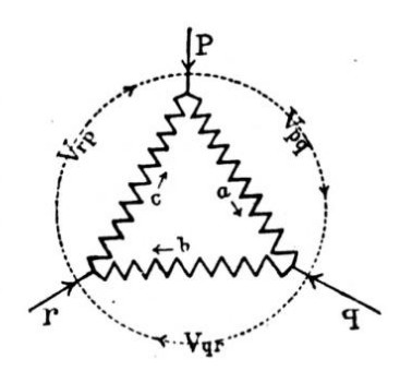
Delta connection is another method to establish three phases of an electrical system. The end terminal of the windings is attached to the starting of the other terminals. Three-line conductors are connected from three junctions. The delta connection is set up by tying the ends. For that we combine a2 with b1, b2 with c1 and c2 with a1. Line conductors are the R, Y, B which run from three junctions. The below image depicts a typical delta connection and shows the end-to-end connections.

Delta Connection
Delta Connection

The relation between phase voltage and the line voltage of the Delta connection

Let us find out the relation between phase voltage of a delta circuit with the circuit’s line voltage. For that, observe the above image carefully. We can say that the value of the voltage at both the terminal 1 and terminal 2 is the same as the terminal R and terminal Y.

So, we can write – E12 = ERY.

In the same way, we can conclude by observing the circuit, E23 = EYE.

And E31 = EBR

The phase voltages are written as: E12 = E23 = E31 = Eph

The line voltages are written as: ERY = EYB = EBR = EL.

So, we can conclude that, in case of a delta connection, the phase voltage will be equal to the circuit’s line voltage.

To know About Kirchhoff’s Laws: Click Here!

The relation between phase current and line current in delta connection

For a balanced delta connection, the constant voltage value affects the current values. The current values of I12, I23, I31 are equal, but they are displaced by 120 degrees from one another. Observe the below-given phasor diagram.

Three phase delta connection
Three phase delta connection, Diagram of Delta Connection, Image Credit – Silvanus Phillips Thompson, Three-phase delta connectionCC0 1.0

We can write, I12 = I23 = I31 = Iph

Now, by applying Kirchhoff’s law at junction 1,

We know that the algebraic sum of the current of a node is zero.

So, I31` = IR` + I12`

The vectoral differences come as IR` = I31` – I12`

By applying vector algebra,

IR = √ (I312 + I122 + 2 * I31 * I12 * Cos 60o)

Or, IR = √ (Iph2 + Iph2 + 2 * Iph * Iph x 0.5)

As, we have discussed earlier, IR = IL.

Or, IL = √ (3Iph2)

Or, IL = √3 * Iph

In the same way, IY` = I12` – I23.`

Or, IL = √ 3 * Iph

And, IB` = I23` – I31`

Or, IL = √ 3 Iph

So, the relation between line current and phase current can be written as:

Line Current = √3 x Phase Current

Difference between Star and Delta Connection

Star and delta methods are two renowned methods for three phase systems. Depending on various factors, there are some fundamental differences between them. Let us discuss some of them.

POINTS OF COMPARISIONSTAR CONNECTIONDELTA CONNECTION
DefinitionThe three terminals are allied at a common point. This type of circuit is called a Star connection.Three end terminals of the circuits are connected with each other to form a closed loop known as delta connection.
Neutral PointThere is a neutral point in star connection.No such neutral point exists in delta connection.
The relation between phase and line voltageLine voltage is calculated as √three times of phase voltage for star connection.Phase voltage and line voltages are equal to each other for delta connections.
The relation between phase current and line currentPhase current and line current for star connection is equal to each other.Line current is √three times of phase current for delta connections.
Speed as startersStar connected motors are usually slower as they get 1/√3 rd of the voltage.Delta connected motors are usually faster as they get the full line voltage.
Phase VoltageThe value of phase voltage for a star connection is lower as they get just 1/√3 part of the line voltage.The value of phase voltage is higher as phase voltage, and line voltages are equal.
Requirement of InsulationLow level of insulation required for a star connection.High level of insulation is required for delta connection.
UsagePower transmission networks use a star connection.Power distribution system uses a delta connection.
The number of turns required.Star connection requires a lesser number of turns.Delta connection requires a higher number of turns.
Received voltageEvery single winding receives 230 volts of voltage in star connection.In delta connection, every single winding receives 414 volts of voltage.
Available systemsStar connection of three wire three phases and four wire three phase systems are available.Delta connection of three wire three phase systems, and four-wire three phase systems are available.

Learn About Basics of AC Circuit: Click Here!

Star delta transformation

Conversion from Star to Delta and Delta to Star

A star network can be converted into a delta network, and a delta connected network can be converted into a star network if needed. Conversion of circuits is necessary to simplify the complicated course, and thus the calculation becomes more effortless.

Conversion from Star to Delta

In this conversion, a connected star network is replaced by its equivalent delta connected network. The star and replaced delta figure are given. Observe the equations.

The value of Z1, Z2, Z3 is given in terms of ZA, ZB, ZC.

Z1 = (ZA ZB + ZB ZC + ZC ZA) / ZC = Σ (ZA ZB) / ZC

Z2 = (ZA ZB + ZB ZC + ZC ZA) / ZB = Σ (ZA ZB) / ZB

Z3 = (ZA ZB + ZB ZC + ZC ZA) / ZA = Σ (ZA ZB) / ZA

We can easily convert a connected star network into a delta connected if we know the star-connected network’s value.

Learn About Advanced AC Circuit: Click Here!

Conversion from Delta to star

In this conversion, a delta connected network is replaced by its equivalent star connected network. The delta and replaced star figure are given. Observe the equations.

The value of ZA, ZB, ZC is given in terms of Z1, Z2, Z3.

ZA = (Z1 Z2) / (Z1 + Z2 + Z3)

ZB = (Z2 Z3) / (Z1 + Z2 + Z3)

ZC = (Z1 Z3) / (Z1 + Z2 + Z3)

We can easily convert a delta connected network into a star connected if we know the value of the delta connected network.

Cover GIF by: GIPHY

Millman’s Theorem: 5 Complete Quick Facts

MT1 300x118 1

Cover Image Credit – RufustelestratSan Diego Reflecting PondCC BY-SA 3.0

Points of Discussions

Introduction to Millman’s Theorem

In the previous Advanced Electrical Circuit Analysis articles, we have discussed some of the fundamental theories like – Thevenin’s Theorem, Norton’s Theorem, Superposition Theorem, etc. We have also come to know the Maximum Power transfer theorem for finding out the maximum load resistance to drain full power. In this article, we will learn about another important and fundamental electrical analysis to deal with complex circuits, known as Millman’s theorem. We will discuss the theory, the process to solve the problems related to this theory, the applications of this theory and other important aspects.

Professor Jacob Millman first proved the theorem, and that is why it is named after him. This theory helps us to simplify the circuit. Thus, it becomes easier to analyze the circuit. This theorem is also known as “Parallel generator theorem”. Millman’s theorem is applied in courses to calculate the voltage of some specified circuitries. It is one of the essential theorems in Electrical Engineering.

What is meant by Thevenin’s theorem? Click Here!

Theory of Millman’s Theorem

Millman’s Theorem: It states that if multiple voltage sources (having internal resistances) are connected in parallel, this specific circuit can be replaced by a simpler circuit of a single voltage source and a resistance in series.

This theory helps us to find out voltages at the end of parallel branches if the circuit is structured in parallel connections. The principal aim of this theory is nothing but to reduce the complexity of the circuit.

Applications of Millman’s Theorem

Millman’s theorem is one of the efficient theorems. That is why there are several real-world applications for this theory. Millman’s theorem is applicable for a circuit with multiple voltage sources with their internal resistances in a parallelly connected way. It helps to solve complex circuit theory problems. Unbalanced bridges, parallel circuit problems can be solved using this theorem.

What are network theorems? Click Here!

Steps for Solving Problems regarding Millman’s Theorem

Generally, the given steps are tracked for solving Millman’s Theory problems. There are several other paths, but following these below-mentioned steps will lead to a more efficient result.

Step 1: Find out the conductance value of every single voltage source.

Step 2: Remove the load resistance. Calculate the equivalent conductance of the circuit.

Step 3: The circuit is now ready to apply Millman’s Theorem. Apply the theorem to find out the equivalent source voltage V. The below equation gives the V value.

V = (± V1 G1 ± V2 G2 ± V3 G3 ± … ±Vn Gn) / G1 + G2 + G3 + … + Gn

V1, V2, V3 are the voltages and G1, G2, G3 are their respective conductance.

Step 4: Now, find out the equivalent series resistance of the circuit with the help of conductance value, calculated earlier. The equivalent series resistance is given by the expression: R = 1 / G

Step 5: At last, calculate the current through the load by the following equation.

IL = V / (R + RL)

Here, IL is the current through the load resistance. RL is the load resistance. R is the equivalent series resistance. V is the identical source voltage calculated with the help of conductance of their respective voltages.

What is Maximum Power Transfer Theorem? Click Here!

Explanation of Millman’s Theorem

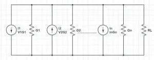
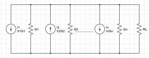
To explain the theorem in details, let us take an example of a specified circuit. The below image describes the needed circuit. The picture shows a typical DC circuit with multiple parallel source voltages with their internal resistances and with the load resistance. RL gives the value of load resistance.

Millman's Theorem
Example Circuit for explanations, Millman’s Theorem, Image – 1

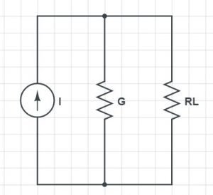
Let us assume that ‘I’ is the current value through the parallel current sources. G gives the equivalent conductance or admittance value. The resultant circuit is shown below.

Millman's Theorem
The resultant circuit, Millman’s Theorem, Image – 2

I = I1 + I2 +I3 + …

G = G1 + G2 + G3 + ….

Now, the final current source is replaced by an equivalent source voltage. The voltage ‘V’ can be written as: V = 1/G = (± I1 ± I2 ± I3 ± … ±In) / (G1 +G2 + G3 + … + Gn)

And equivalent series resistance comes as:

R = 1 / G = 1 / (G1 + G2 + G3 + … + Gn)

Now, we know that V = IR and R = 1 / G

So, V can be written as:

V = [± (V1 / R1) ± (V2 / R2) ± (V3 / R3) ± … ± (Vn / Rn)] / [ (1 / R1) ± (1 / R2) ± (1 / R3) ± … ± (1 / Rn)]

R is the equivalent series resistance.

Now, as per Millman’s theory, the equivalent voltage source comes to be:

V = (± V1 G1 ± V2 G2 ± V3 G3 ± … ±Vn Gn) / (G1 + G2 + G3 + … + Gn)

Or, V = Σ (n, k = 1) Vk Gk / Σ (n, k = 1) Gk

Gk = 1 /Rk

To know About Kirchhoff’s Laws: Click Here!

Solved Problems on Millman’s Theorem

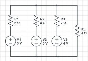
1. A complex circuit is given below. Find the current through the 4 ohms resistance. Use Millman’s Theorem to solve the problem.

Millman's Theorem
Problem – 1, Millman’s Theorem, Image – 3

Solution: We will solve the problem by following the previously mentioned steps.

So, we have to find out the voltage value and the equivalent resistance value.

We know that the voltage is given by,

V = [± (V1 / R1) ± (V2 / R2) ± (V3 / R3) ± … ± (Vn / Rn)] / [ (1 / R1) ± (1 / R2) ± (1 / R3) ± … ± (1 / Rn)]

Here, we have three voltage source and three resistances. So, the updated equation will be,

VAB = [± (V1 / R1) ± (V2 / R2) ± (V3 / R3)] / [ (1 / R1) ± (1 / R2) ± (1 / R3)]

VAB = [(5 / 6) + (6 / 4) + (4 / 2)] / [(1 / 6) + (1 / 4) + (1 / 2)]

VAB = 4.33 / 0.9167

OR, VAB = 4.727 V

Now, we have to calculate the equivalent resistance of the circuit, or the Thevenin’s equivalent resistance is Rth.

RTH = [(1 / 6) + (1 / 4) + (1 / 2)] -1

Or, RTH = 1.09 ohms

At the last step, we will find out the current value through the load resistance, that is 4 ohms.

We know that, IL = VAB / (RTH + RL)

Or, IL = 4.727 / (1.09 + 4)

Or, IL = 4.727 / 5.09

Or, IL = 0.9287 A

So, The load current through 4 ohms load is 0.9287 A.

Learn About Basics of AC Circuit: Click Here!

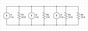
2. A complex electrical circuit is given below.  Find out the current through the 16 ohms load resistance. Use Millman’s theorem to solve the problems.

Millman's Theorem
Problem – 2, Millman’s Theorem, Image – 4

Solution: We will solve the problem by following the previously mentioned steps.

At first, we have to calculate the current value using Norton’s theorem.

The current ‘I’ can be written as: I = I1 + I2 + I3

Or, I = 10 + 6 – 8

Or, I = 8 A

Now we have to find out the Equivalent resistance value. We represent the equivalent resistances of R1, R2, R3 as RN.

So, RN = [(1 / R1) + (1 / R2) + (1 / R3)]-1

Or, RN = [(1/ 24) + (1 / 8) + (1 / 12)]-1

Or, RN = 4 ohms

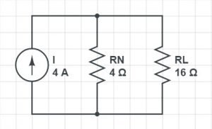
We now redraw the circuit with equivalent voltage and resistances value and place the circuit’s load resistance.

Millman's Theorem
Equivalent Circuit, Millman’s Theorem, Image – 5

At the last step, we have to find out the load Current. So, IL = I x R / (R + RL)

Or, IL = 8 x 4 / (4 + 16)

Or, IL = 1.6 A.

So, the load current through the 8 ohms load resistor is 1.6 A.

Learn About Advanced AC Circuit: Click Here!

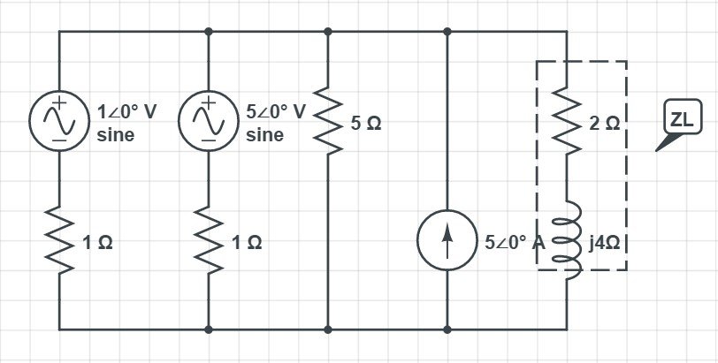
3. A complex AC network is given below.  Compute the current passing through the Load ZL. Use Millman’s Theorem to solve the problem.

Millman's Theorem
Problem – 3, Millman’s Theorem Image – 6

Solution: We will solve the problem by following the previously mentioned steps. In this problem, we can see that a current source is given. But we know that we cannot apply Millman’s Theory for a current source. So, It is possible to  convert the current source to a voltage source.

Now, we apply Millman’s theorem and finds out the equivalent voltage.

We know that,

V = [± (V1 / R1) ± (V2 / R2) ± (V3 / R3)] / [ (1 / R1) ± (1 / R2) ± (1 / R3)]

So, V = (1 * 1 ∠0o + 1 * 5 ∠0o + 0.2 * 25 ∠0o) / ( 1 + 1 + 0.2)

Or, V = 11 / 2.2 = 5 ∠0o V.

IL gives the current through the load resistance.

As we know, V = IR.

Or, IL = V / ZL = 5 ∠0o / (2 + j4)

Or, IL = 1.12 ∠-63.43o A.

So, Current through the load resistance is 1.12 ∠-63.43o A.  

Cover Photo By: Abyss

Maximum Power Transfer Theorem | 3+ Important Steps| Explanations

MPT1 300x203 1

Image Credit: Iñigo Gonzalez from Guadalajara, Spain, Lamp @Ibiza (624601058)CC BY-SA 2.0

Points of Discussion

Introduction to Maximum Power Transfer Theory

In the previous articles related to circuit analysis, we have come across several methods and theories regarding solving problems of a complex network. The maximum power transfer theorem is one of the efficient theories needed to analyze and study advanced circuits. It is one of the primary methods yet important one.

We will discuss the theories, the problem-solving steps, real-world applications, the explanation of the theory. A mathematical problem is solved at last for a better understanding.

Know about: Thevenin’s Theorem! Click Here!

Theory of Maximum Power Transfer Theorem

Maximum power Transfer Theory:

It states that a DC Circuit’s load resistance receives the maximum power if the magnitude of the load resistance is the same as the Thevenin’s equivalent resistance.

The theory is used to calculate the value of load resistance, which causes the maximum power transferred from the source to the load. The theorem is valid for both AC and DC circuits (Point to be noted: For AC circuits, the resistances are replaced by impedance).

Real world Applications of Maximum power transfer theorem

The maximum power transfer theorem is one of the efficient theorems. That is why there are several real-world applications for this theory. The communication sector is one of its fields. The theory is used for low strength signals. Also, for loud speakers to drain the maximum power from the amplifier.

Know about: Norton’s Theorem! Click Here!

Steps for solving problems regarding Maximum Power Transfer Theorem

In general, the below mentioned steps are followed for solving power transfer theory problems. There are other ways, but following these steps will lead to a more efficient path.

  • Step 1: Find out the load resistance of the circuit. Now remove it from the circuit.
  • Step 2: Calculate the Thevenin’s equivalent resistance of the circuit from the open circuited load resistance branch’s view point.
  • Step 3: Now, as the theory says, the new load resistance will be the Thevenin’s equivalent resistance. This is the resistance that is responsible for Maximum power transfer.
  • Step 4: The maximum power is derived then. It comes as follows.

PMAX = VTH2 / 4RTH

Know about: Superposition Theorem! Click Here!

Explanations of the Maximum Power Transfer Theory

To explain the theorem, let us take a complex network as below.

Maximum Power Transfer Theorem - 1
Example :Thevenin’s equivalent Circuit, Maximum Power Transfer Theorem – 1

In this circuit, we have to calculate the value of load resistance for which the maximum power will be drained from the source to the load.

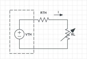
As we can see in the above images, the variable load resistance is attached to the DC circuit. In the second image, the Thevenin’s equivalent circuit is already represented (both the Thevenin’s equivalent circuit and Thevenin’s equivalent resistance).  

From the second image, we can say current (I) through the circuit is:

I = VTH / (RTH + RL)

The power of the circuit is given by P = VI.

Or, P = I2 RL

Substituting the value of I from the Thevenin’s equivalent circuit,

PL = [VTH / (RTH + RL)]2 RL

We can observe that the value of PL can be increased or preferably varied by changing RL‘s value. According to the rule of calculus, the maximum power is achieved when the derivative of the power with respect to the load resistance is equal to zero.

 dPL / dRL = 0.

Differentiating PL, we get,

dPL / dRL = {1 / [(RTH + RL)2]2} * [{(RTH + RL)2 d/dRL (VTH2 RL)} – {(VTH2 RL) d/dRL (RTH + RL)2}]

Or, dPL / dRL = {1 / (RTH + RL)4} * [{(RTH + RL)2 VTH2} – {VTH2 RL * 2 (RTH + RL)

Or, dPL / dRL = [VTH2 * (RTH + RL – 2RL)] / [(RTH + RL)3]

Or, dPL / dRL = [VTH2 * (RTH – RL)] / [(RTH + RL)2]

For the maximum value, dPL / dRL = 0.

So, [VTH2 * (RTH – RL)] / [(RTH + RL)2] = 0

From which, we get,

(RTH – RL) = 0 or, RTH = RL

It is now proved that the maximum power will be drawn when the load resistance and internal equivalent resistance are the same.

So, the maximum power which can be drawn by any circuit,

PMAX = [VTH / (RTH + RL)]2 RL

Now, RL = RTH

OR, PMAX = [VTH / (RTH + RTH)]2 RTH

OR, PMAX = [VTH2 / 4RTH2] RTH

OR, PMAX= VTH2 / 4RTH

This is the power drawn by the load. The power received by the load is the same power send by the load.

So, the total supplied power is:

P = 2 * VTH2 / 4RTH

Or, P = VTH2 / 2RTH

The efficiency of the power transfer is calculated as follows.

η = (PMAX / P) * 100 % = 50 %

This theory aims to gain the maximum power from the source by making the load resistance equal to the source resistances. This idea has different and several applications in the field of communication technology, especially the signal analysis part. The source and load resistances are matched previously and decided before the circuit operation started to attain the maximum power transfer condition. The efficiency comes down to 50%, and the flow of power started from source to load.

Now, for electrical power transmission systems, where the load resistances have higher values than the sources, the condition of maximum power transfer is not achieved easily. Also, the efficiency of the transfer is just 50%, which has no good economical values. That is why the power transfer theorem is rarely used in the power transmission system.

Know about: KCL, KVL Theorems! Click Here!

Problems Related to Maximum Power Transfer Theorem

Observe the circuit carefully and calculate the resistance value to receive the maximum power. Apply maximum power transfer theorem to find out the amount of power transferred.

Maximum Power Transfer Theorem - 2
Circuit, Maximum Power Transfer Theorem – 2

Solution: The problem is solved by following the given steps.

In the first step, the load resistance is disconnected from the circuit. After disconnecting the load, we mark it as AB. In the next step, we will calculate the Thevenin’s equivalent voltage.

Maximum Power Transfer Theorem - 3
The load is removed, Maximum Power Transfer Theorem – 3

So, VAB = VA – VB

VA comes as: VA = V * R2 / (R1 + R2)

Or, VA = 60 * 40 / (30 + 40)

Or, VA = 34.28 v

VB comes as:

VB = V * R4 / (R3 + R4)

Or, VB = 60 * 10 / (10 + 20)

Or, VB = 20 v

So, VAB = VA – VB

Or, VAB = 34.28 – 20 = 14.28 v

Now, it is time to find out the Thevenin’s equivalent resistance for the circuit.

For that, we short circuit the voltage source and the resistance values are calculated through the open terminal of the load.

RTH = RAB = [{R1R2 / (R1 + R2)} + {R3R4 / (R3 + R4)}]

OR, RTH = [{30 × 40 / (30 + 40)} + {20 × 10 / (20 + 10)}]

OR, RTH = 23.809 ohms

Maximum Power Transfer Theorem - 4
Calculation of resistances, Maximum Power Transfer Theorem – 4

Now the circuit is redrawn using the equivalent values. The maximum power transfer theorem says that to obtain the maximum power, the load resistance = Thevenin’s equivalent resistance. So as per the theory, load resistance RL = RTH = 23.809 ohms.

Maximum Power Transfer Theorem - 5
Final Equivalent Circuit, Maximum Power Transfer Theorem – 5

Formula for the maximum power transfer is PMAX = VTH2 / 4 RTH.

Or, PMAX = 14.282 / (4 × 23.809)

Or, PMAX = 203.9184 / 95.236

Or, PMAX = 2.14 Watts

So, the maximum amount of transferred power is 2.14 watts.

Know about: Circuit Analysis! Click Here!

2. Observe the circuit carefully and calculate the resistance value to receive the maximum power. Apply maximum power transfer theorem to find out the amount of power transferred.

Maximum Power Transfer Theorem - 6
Circuit for Problem No. 2, Maximum Power Transfer Theorem – 6

Solution: The problem is solved by following the given steps.

In the first step, the load resistance is disconnected from the circuit. After disconnecting the load, we mark it as AB. In the next step, we will calculate the Thevenin’s equivalent voltage. VTH = V * R2 / (R1 + R2)

VTH = V * R2 / (R1 + R2)

Or, VTH = 100 * 20 / (20 +30)

Or, VTH = 4 V

Now, it is time to find out the Thevenin’s equivalent resistance for the circuit. The resistances are in parallel with each other.

So, RTH = R1 || R2

Or, RTH = 20 || 30

Or, RTH = 20 * 30 / (20 + 30)

Or, RTH = 12 Ohms

Now the circuit is redrawn using the equivalent values. The maximum power transfer theorem says that to obtain the maximum power, the load resistance = Thevenin’s equivalent resistance. So as per the theory, load resistance RL = RTH = 12 ohms.

Formula for the maximum power transfer is PMAX = VTH2 / 4 RTH.

Or, PMAX = 1002 / (4 × 12)

Or, PMAX = 10000 / 48

Or, PMAX = 208.33 Watts

So, the maximum amount of transferred power is 208.33 watts.

Check out Our Latest releases on Electronics Engineering.

.

3 Important Theorems On Electrical Circuit Analysis

TH1 300x152 1

Points of Discussion: Electrical Circuit Analysis

Introduction to Advanced Electrical Circuit Analysis

We came to know the primary circuit structure and some essential terminologies in the previous circuit analysis article. In the DC Circuit analysis, we have studied KCL, KVL. In this article, we are going to learn about some advanced methods for circuit analysis. They are – Superposition theorem, Thevenin’s theorem, Norton’s theorem. There are many more methods for circuit analysis like – maximum power transfer theory, Millman’s theory, etc.

We will learn about the theory of the methods, the detailed explanation of the theory and steps for solving circuit problems.

Basic Terminologies Related to Circuit Analysis : Click Here!

Advanced Electrical Circuit Analysis: Thevenin’s Theorem

Thevenin’s theorem (Helmholtz – Thevenin theorem) is one of the most crucial theories needed for analysing and studying complex circuits. It is one of the simplest methods to solve complex network problems. Also, it is one of the most widely used methods for circuit analysis.

Thevenin’s Theorem: It states that all complex networks can be replaced by a voltage source and a resistance in series connection.

In simpler words, if a circuit has energy sources like dependent or independent voltage sources, and has a complex structure of resistances, then the whole circuit is representable as a circuit consisting the equivalent voltage source, the load resistance, and the equivalent resistance of the circuit, all in series connection.

Steps for solving problems regarding Thevenin’s theorem

  • Step 1: Remove the Load Resistance and redraw the circuit. (Note: The load resistance will be the referenced resistance through which you have to calculate the current).
  • Step 2: Find out the open circuit voltage or Thevenin’s equivalent voltage for the circuit.
  • Step 3: Now short circuit all the voltage sources, and open circuit all the current sources. Also, substitute all the elements with their equivalent resistances and redraw the circuit (Note: Keep the load resistance is unattached).
  • Step 4: Find out the equivalent resistance of the circuit.
  • Step 5: Draw a fresh circuit with a voltage source and two resistance in series with it. The magnitude of the voltage source will be the same as the derived equivalent Thevenin’s voltage. One of the resistances will be the pre-calculated equivalent resistance, and the other is the load resistance.
  • Step 6: Calculate the current through the circuit. That is the final answer.

Explanation

To explain the theorem, let us take a complex circuit as below.

Electrical circuit analysis
Example Circuit, Electrical Circuit Analysis – 1

In this circuit, we have to find out the current I, through the resistance RL using the Thevenin’s theorem.

Now, to do so, first remove the load resistance and make that branch open circuited. Find out the open circuit voltage or Thevenin’s equivalent across that branch. The open circuited voltage comes as: VOC = I R3 = (VS / R1 + R3) R3

TH2
The Load is removed, Electrical Circuit Analysis – 2

For calculation of the equivalent resistance, the voltage source is short circuited (deactivated). Now, find out the resistance. The equivalent resistance comes out as: RTH = R2 + [(R1 R3) / (R1 + R3)]

TH3
The voltage source is short circuited & the equivalent resistance is calculated, Electrical Circuit Analysis – 3

At the last step, make a circuit using the derived equivalent voltage and equivalent resistance. Connect the load resistance in series with the equivalent resistance. 

The current comes as: IL = VTH / (RTH + RL)

TH4
Thevenin’s Equivalent Circuit, Electrical circuit Analysis – 4

Electrical Circuit Analysis: Norton’s Theorem

Norton’s theorem (Mayer – Norton Theorem) is another crucial theory needed to analyses and study complex circuits. It is one of the simplest methods to solve complex network problems. Also, it is one of the most widely used methods for circuit analysis.

Norton’s Theorem: It states that all complex networks can be replaced by a current source and a resistance in parallel connection.

In simpler words, if a circuit has energy sources like dependent or independent current sources, and has a complex structure of resistances, then the whole circuit is representable as a circuit consisting the equivalent current source, the load resistance, and the equivalent resistance of the circuit, all in parallel connection.

Steps for solving problems regarding Norton’s theorem

  • Step 1: Short circuit the Load Resistance and redraw the circuit. (Note: The load resistance will be the referenced resistance through which you have to calculate the current).
  • Step 2: Find out the short circuit current or Norton’s current of the circuit.
  • Step 3: Now, short circuit all the independent sources. Also, substitute all the elements with their equivalent resistances and redraw the circuit (Note: Make the load resistance unattached).
  • Step 4: Find out the equivalent resistance of the circuit.
  • Step 5: Draw a fresh circuit with a current source and two resistance in parallel with it. The magnitude of the current source will be the same as the derived equivalent short-circuit current. One of the resistances will be the pre-calculated equivalent resistance, and the other is the load resistance.
  • Step 6: Calculate the current through the circuit. That is the final answer.

Explanation

To explain the theorem, let us take a complex circuit as below.

TH1 1
Example Circuit, Electrical Circuit Analysis – 5

In this circuit, we have to find out the current I, through the resistance RL using Norton’s theorem.

To do so, first, remove the load resistance (RL) and make that branch short circuited. The current in the closed loop is calculated first.

I = VS / [ R1 + {R2R3/ (R2 + R3)}]

The short circuit current comes as ISC = I R3 / (R3 + R2)

NT2
Load is removed and short circuited, Electrical circuit analysis – 6

The voltage source is short circuited (deactivated) and the load resistance branch is short circuited for calculation of the equivalent resistance. Now, find out the resistance. The equivalent resistance comes out as: RNT = R2 + [(R1 R3) / (R1 + R3)]

NT3
Equivalent Resistances, Electrical circuit analysis – 7

At the last step, make a circuit using the derived equivalent current source and equivalent resistance. Connect the load resistance in parallel with the equivalent resistance and the current source in parallel with them. 

The current comes as: IL = ISC RNT / (RNT + RL)

NT4
Norton’s Equivalent Circuit, Electrical circuit Analysis – 8

Electrical Circuit Analysis: Superposition Theorem

Superposition theorem is another crucial theory needed for analysing and studying of complex circuits. It is another easy method to solve complex network problems. Also, it is one of the most widely used methods for circuit analysis. Superposition theory is only applicable for linear circuits and circuits which obey Ohm’s law.

Superposition Theorem: It states that for all active, linear circuits, which have multiple sources, the response across any circuit element, is the aggregate sum of the responses obtained from each source considered separately and every source are substituted by their internal resistances.

In a more general way, the theorem states that the aggregate current in each branch can be expressed as the sum of all currents produced for a linear network. At the same time, all the source acted separately, and their internal resistances substitute independent sources.

Steps for solving problems regarding superposition theorem

  • Step 1: Consider one independent source at a time and deactivate (short-circuit) all the other sources.
  • Step 2:  Replace that other source with the equivalence of the resistors of the circuits. (Note: By default, if the resistance is not given, make it short-circuit).
  • Step 3: Now, short circuit all the other (leave the selected source) voltage source and open circuit all the other current source. 
  • Step 4: Find the current for every branch of the circuit.
  • Step 5: Now choose another voltage source and follow step 1-4. Please do it for every independent source.
  • Step 6: At last, calculate the current for each branch by superposition theorem (addition). To do so, add up currents of the same branch calculated for different voltage sources. Add the direction of the currents wise (if the same direction – add up, else minus).

Explanation

To explain the method, let us take a complex circuit as below.

SP1
Superposition Theorem Circuit, Electrical circuit Analysis – 9

In this circuit, we have to find out the current through each branch. The circuit has two voltage sources.

At first, we choose the V1 source. So, we short circuit (as the source’s internal resistance is not given) the other voltage source – V2.

SP2 1
One source is removed, Electrical circuit Analysis – 10

Now, calculate all the current for every branch. Let the current through the branches are – I1`, I2`, I3`. They are represented as follow.

I1` = V1 / [ R1 + {R2R3/ (R2 + R3)}]

I2` = I1` R3 / (R3 + R2)

Now, I3` = I1` – I2`

The V2 voltage source is activated in the next step while the V1 source is deactivated or short circuited (internal resistance is not given).

SP3
Another Source is removed, Electrical circuit Analysis – 11

As the previous step, here we need to calculate the current for every branch again. The current through the branches comes as follow.

I2“ = V2 / [ R2 + {R1R3/ (R1 + R3)}]

I1“ = I2“ R3 / (R3 + R1)

Now, I3“ = I2“ – I1

SP5
Current in the branches, Electrical circuit Analysis – 12

All the source calculation is now covered. Now, we have to apply superposition theorem and find out the net currents for the branches. The direction rule is considered while calculating. The I1, I2, I3 magnitudes are given below.

I3 = I3` + I3

I2 = I2` – I2

I1 = I1` – I1

For mathematical problems, check out the next article.

AC Circuit Analysis: 3 Important Facts You Should Know

RC Series 300x159 1

Points of Discussions: AC Circuit Analysis

Introduction to Advanced AC Circuit Analysis

In the previous article of the AC circuit, we have discussed some of the basic ac circuit analysis. We have studied about the circuit, the phasor diagrams, power calculations, and some essential terminologies. In this article, we will learn some advanced AC circuit analysis like – RC Series circuit, RL series circuit, RLC series circuit, etc. These advanced circuits are essential and have more applications in electrical analysis. All of these circuits can be said another level of primary ac circuit as the more complex circuit can be built using these. Please check out the introductory circuit article before studying this advanced ac circuit analysis.

Basic AC Circuit Analysis: Read Here!

RC Series Circuit

If a pure resistor is placed in a series with a pure capacitor in an AC circuit, then the ac circuit will be called RC AC Series Circuit. An ac voltage source produces sinusoidal voltages and the current passes through the resistor and the capacitor of the circuit.

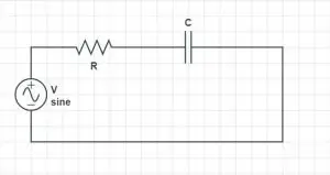
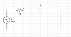
  • Circuit diagram of RC series circuit
RC Series Circuit, AC circuit analysis
RC Series Circuit, AC Circuit analysis – 1

VR gives the voltage across the resistance, and – VC gives the voltage across the capacitor. The current through the circuit is I. R is the resistance and C is the capacitance value. XC denotes the capacitive reactance of the capacitor.

Widerstand ZeigerRC 1
phasor diagram of RC series Circuit, Ac circuit analysis – 2, Image Credit – Saure at German WikipediaWiderstand ZeigerRCCC BY-SA 3.0

The process to draw the phasor diagram of RC Circuit.

The phasor diagram is an essential analytical tool which helps to study the behaviour of the circuit. Let us learn the steps to draw the phasor.

Step 1. Find out the r.m.s value of the current. Mark that as the reference vector.

Step 2. As we know that for a purely resistive circuit, voltage and current remains in the same phase, here as well voltage drop across the resistor stays in phase with the current value. It is given as V = IR.

Step 3. Now for the capacitive circuit, we know that voltage lags by 90 degrees and current leads. That is why voltage drop across the capacitor in this circuit, stays 90 degrees behind than the current vector.

Step 4. The applied voltage thus comes as the vector sum of the voltage drops of capacitor and resistances. So, it can be written as:

V2 = VR2 + VC2

Or, V2 = (IR)2 + (IXC)2

Or, V = I √ (R2 + XC2)

Or, I = V / √ (R2 + XC2)

Or, I = V / Z

Z is the aggregate impedance of the RC circuit. The following equation represents the mathematical form.

Z = √ (R2 + XC2)

Now from the phasor diagram, we can observe there is an angle as – ϕ.

So, tan ϕ will be equal to IXC / IR.

So, ϕ = tan-1 (IXC / IR)

This angle ϕ is known as phase angle.

  • RC Series Circuit Power calculation

The power of the circuit is calculated by P = VI formula. Here we will calculate the instantaneous value of power.

So, P = VI

Or, P = (Vm Sinωt) * [Im Sin (ωt+ ϕ)]

Or, P = (Vm Im / 2) [ 2Sinωt * Sin (ωt+ ϕ)]

Or, P = (Vm Im / 2) [ cos {ωt – (ωt+ ϕ)} – cos {ωt – (ωt+ ϕ)}]

Or, P = (Vm Im / 2) [ cos (- ϕ) – cos (2ωt+ ϕ)]

Or, P = (Vm Im / 2) [ cos (ϕ) – cos (2ωt+ ϕ)]

Or, P = (Vm Im / 2) cos (ϕ) – (Vm Im / 2) cos (2ωt+ ϕ)

We can observe that the power equation has two sections. One is a constant part another is the variable section. The mean of the variable part comes to be zero over a full cycle.

So, the average power for an RC series circuit, over a full cycle is given as :

P = (Vm Im / 2) cos (ϕ)

Or, P = (Vm / √2) * (Im / √2) * cos (ϕ)

Or, P = VI cos (ϕ)

Here, V and I are considered as RMS values.

The power factor of RC Series Circuit

The RC series circuit’s power factor is given by the ratio of active power to the apparent power. It is represented by cosϕ and expressed as below given expression.

cos ϕ = P / S = R / (R2 + XC2)

RL Series Circuit

If a pure resistor is placed in a series with a pure inductor in an AC circuit, then the ac circuit will be called RL AC Series Circuit. An ac voltage source produces sinusoidal voltages and the current passes through the resistor and the inductor of the circuit.

  • Circuit Diagram of RL circuit
RL
RL Series Circuit, AC Circuit analysis – 3

VR gives the voltage across the resistance, and – VL gives the voltage across the inductor. The current through the circuit is I. R is the resistance and L is the inductance value. XL denotes the inductive reactance of the inductor.

  • Phasor Diagram of RL circuit
RL IU Zeiger
RL Circuit Phasor Diagram, AC Circuit Analysis – 4, Image Credit – SaureRL I(U)-ZeigerCC BY-SA 3.0

The process to draw the phasor diagram of RL Circuit.

Step 1. Find out the r.m.s value of the current. Mark that as the reference vector.

Step 2. As we know, for a purely resistive circuit, voltage and current remain in the same phase, here as well voltage drop across the resistor stays in phase with the current value. It is given as V = IR.

Step 3. Now for the inductive circuit, we know that voltage leads by 90 degrees and the current lags. That is why voltage drop across the inductor in this circuit, stays 90 degrees ahead than the current vector.

Step 4. The applied voltage comes as the vector sum of the voltage drops of inductor and resistances. So, it can be written as:

V2 = VR2 + VL2

Or, V2 = (IR)2 + (IXL)2

Or, V = I √ (R2 + XL2)

Or, I = V / √ (R2 + XL2)

Or, I = V / Z

Z is the aggregate impedance of the RL circuit. The following equation represents the mathematical form.

Z = √ (R2 + XL2)

Now from the phasor diagram, we can observe there is an angle as – ϕ.

So, tan ϕ will be equal to IXL / IR.

So, ϕ = tan-1 (XL / R)

This angle ϕ is known as phase angle.

  • RL Series Circuit Power calculation

The power of the circuit is calculated by P = VI formula. Here we will calculate the instantaneous value of power.

So, P = VI

Or, P = (Vm Sinωt) * [Im Sin (ωt- ϕ)]

Or, P = (Vm Im / 2) [ 2Sinωt * Sin (ωt – ϕ)]

Or, P = (Vm Im / 2) [ cos {ωt – (ωt – ϕ)} – cos {ωt – (ωt – ϕ)}]

Or, P = (Vm Im / 2) [ cos (ϕ) – cos (2ωt – ϕ)]

Or, P = (Vm Im / 2) cos (ϕ) – (Vm Im / 2) cos (2ωt – ϕ)

We can observe that the power equation has two sections. One is a constant part another is the variable section. The mean of the variable part comes to be zero over a full cycle.

So, the average power for an RL series circuit, over a full cycle is given as :

P = (Vm Im / 2) cos (ϕ)

Or, P = (Vm / √2) * (Im / √2) * cos (ϕ)

Or, P = VI cos (ϕ)

Here, V and I are considered as RMS values.

LC Series Circuit

An LC series circuit is an AC circuit consisting of inductor and capacitor, placed in a series connection. An LC circuit has several applications. It is also known as a resonant circuit, tuned circuit, LC filters. As there is no resistor in the circuit, ideally this circuit doesn’t suffer any losses.  

LC Circuit as Tuned Circuit: The flow of current means flows of charges. Now in an LC circuit, charges keep flowing behind and ahead of the capacitor plates and through the inductor. Thus, a type of oscillation gets created. That is why these circuits are known as tuned or tank circuit. However, the internal resistance of the circuit prevents the oscillation in real.

  • Circuit diagram of LC Series Circuit
LC
Series LC Circuit, Tank circuit, Ac Circuit Analysis

In a series circuit, the current value is the same across the whole circuit. So we can write that, I = IL = IC.

The voltage can be written as V = VC + VL.

  • Resonance in series LC Circuit

Resonance is refereed to as a particular condition of this LC circuit. If the frequency of the current increases, the value of inductive reactance also gets increased, and the value of capacitive reactance gets decreased.

XL = ωL = 2πfL

XC = 1 / ωC = 2πfC

At the resonance condition, the magnitude of capacitive reactance and inductive reactance is equal. So, we can write that XL = XC

Or, ωL = 1 / ωC

Or, ω2C = 1 / LC

Or, ω = ω0 = 1 / √LC

Or, 2πf = ω0 = 1 / √LC

Or, f0 = ω0 / 2π = (1/2π) (1 / √LC)

f0 is the resonant frequency.

  • The impedance of the circuit

Z = ZL + ZC

Or, Z = jωL + 1 / jωC

Or, Z = jωL + j / j2ωC

Or, Z = jωL – j / ωC

Circuit Analysis: 5 Complete Quick Facts

1280px Resistor symbol America.svg 300x113 1

Cover Image Credit – Santeri Viinamäki, MCB Circuit breakers for DIN railCC BY-SA 4.0

Points of discussion : Circuit Analysis

Introduction to Circuit Analysis

Circuit analysis is one of the primary and essential modules for Electrical and Electronics Engineering. Before exploring out the concepts and theories of circuit analysis, let us know what a circuit is.

A circuit can be defined as a closed or open loop consists of electrical and electronic components and have interconnection between them. Circuit analysis is the method to determine the necessary current or voltage value at any point of the circuit by studying and analysing the circuit. There are numerous different methods for circuit analysis and used as per suitable conditions.

What is a DC Circuit? Learn About KCL & KVLs! Click Here!

Ideal Circuit Elements

An ideal circuit can be defined as a circuit without any losses, thus the appearance of 100% input power at the output side. An ideal circuit consists of three ideal elements. They are – Resistances, capacitor, Inductor.

  • Resistors: Resistors are passive electrical components used to resist the flow of electrons in a circuit. The voltage across the resistor is expressed by a famous law, known as Ohm’s law. It states that “the voltages are directly proportional to the currents”. If V and I respectively denote the voltage value and current, then

V ∝ I

Or, V = IR

Here R represents the resistance or resistor value. The unit is given by ohm(Ω).  The following image

represents the resistor –

Resistor Symbol, Circuit analysis image - 1
Resistor Symbol, Circuit analysis image – 1

The following mathematical expression gives the power stored by a resistor.

P = VI

Or, P = (IR) I

Or, P = I2R

Or, P = V2 / R

  • Capacitor: A typical capacitor is a passive electrical equipment which stores electrical energy inside an electric field. It is a two-terminal device. Capacitance is known as the effect of the capacitor. Capacitance has a unit – Farad(F). The capacitor is represented in the circuit by the following image.
1120px Capacitor Symbol.svg
Capacitor Symbol, Circuit Analysis, Image – 2

The relation between charges and capacitance is given by Q = CV, where C is the capacitance value, Q is the Charge, V is the applied voltage.

The current relationship can be derived from the above equation. Let us differentiate both side with respect to time.

dQ/dt = C dV/dt; C is a constant value

Or, I = C dV/dt; as I = dQ/dt.

Power stored in a capacitor can be described written as

P = VI

Or, P = V C dV/dt

Now, the energy is given as U = ∫ p dt

Or, U = ∫ V C (dV/dt) dt

Or, U = C ∫ V dV

If we assume that the capacitor was discharged at the beginning of the circuit, then the power comes as U = ½ CV2.

  • Inductor: Inductor is another passive device present in an ideal circuit. It holds energies in a magnetic field. The unit of inductance is given by Henry(H). The relation between voltage and inductance is given below.

V = L dI/dt

The reserved energies are returned back to the circuitry in current form. The following image represents the inductor in the circuit.

1280px Inductor symbol.svg
Inductor Symbol, Circuit Analysis, image – 3

The power of an inductor is given as P =VI.

Or, P = I * L (dI/dt)

Again, the energy U = ∫ p dt

Or, U = ∫ I * L (dI/dt) dt

Or, U = L ∫ I dI

The energy comes as U = ½ LI2.

Learn about different types of AC Circuits! Click here!

Realistic Circuit Elements

Ideal circuit components are for ideal circuits. They are not applicable in real circuits. However, the main characteristics remain the same for the elements. Elements suffer some loss, have some tolerance values and some abstractions while using it.

The working principles and equations get changed in real domains. Also, some other factors get added during operations. For example, capacitors work differently in high-frequency domains; resistors generate a magnetic field during operations.

  • Resistors: The real-world resistors should be made to obey Ohm’s law as close as they can. The resistance offered by a resistor depends upon the material and shape of the resistor.

A real resistor maybe gets destroyed or burned out due to heat generated by itself. There is a certain tolerance level mentioned for every resistor via the color codes.

  • Capacitors: The realistic capacitors should be made to obey the capacitor’s equation as close as possible. Two conducting surfaces are needed to build a capacitor. They are placed together, and air or any material is filled in between them. The capacitor value is dependent on the surface area of the conductor and the distance between them and upon the permittivity of the inside material. There are various categories of capacitors in the market. Some of them are – Electrolytic Capacitors, Tantalum Capacitors, etc.

Capacitors are connected with wire at their terminals. That causes resistance and a small amount of impedance. An increase in voltage across the capacitors sometimes damages the insulative materials between the plates.

  • Inductors: The realistic or real-world inductors should be made to obey the inductor equation as close as possible. Inductors are choke of coils. They induce magnetic fields to store electrical-energies.

Inductors are made using the winding wires in a coil-like structure: the more the winding, the stronger the magnetic field. Placing a magnetic material inside the coil would increase the magnetic effect. Now, as these wires are wounded around the material, this causes the generation of resistance. Also, it is needed to be large enough to accumulate the magnetic field. That sometimes causes problems.

Ideal Energy Sources

An ideal circuit needs an ideal source of energy. There are two types of ideal energy sources. They are – ideal voltage source and ideal current source.

Ideal Voltage Source: Ideal voltage sources supply a constant amount of voltage for every instant of time. Voltage is constant throughout the source. In reality, there is no ideal source for circuits. It is an assumption to simplify the circuit analysis. The below image represents an ideal voltage source.

Ideal voltage source symbols
Three symbols for ideal voltage source, Circuit analysis image – 4, Image credit – Hardman FeidlimidIdeal voltage source symbolsCC BY-SA 4.0

Ideal Current Source: Ideal current sources supply currents independent of the variation of voltage in the circuit. An ideal current source is an approximation that does not take place in reality but can be achieved. The below picture represents the ideal current source in a circuit.

1024px Current Source.svg
Ideal Current source, Circuit analysis, image – 5

Real energy sources for circuits

Real electrical or electronic circuits need natural sources of energy. There are some differences between ideal and real-world energy sources though the main principle of supplying the energy to the circuit remains the same. Real-world energy sources have several types. Some are even dependent upon other sources. Like – Voltage controlled current source, Current controlled current source, etc. We will discuss them briefly in this circuit analysis article.

  • Voltage Sources: Real voltage sources come up with an internal resistance, which is consider it to be in series with the voltage source. No matter how negligible the resistance is, it affects the V-I characteristic of the circuit. The voltage source can be of two types –
  1. Independent Voltage Source
  2. Dependent Voltage Source

Independent Voltage Sources: These voltage sources have no dependency upon any other energy sources of the circuit. It provides a small resistance, which changes the V-I characteristic plot.

Dependent Voltage Sources: These voltage sources are dependent upon any other energy sources present in the circuits. They can be classified into two categories

  • Voltage Controlled Voltage Source
  • Current Controlled Voltage Source.
  • Voltage Controlled Voltage Source: If any other voltage source is controlled by any kind of voltage source, it is known as Voltage controlled voltage source. V0 = AVc gives voltage output; Here, A represents the gain, and Vc is the controlling voltage.
  • Current Controlled Voltage Source: If any other voltage source is controlled by different current source in the circuit, it is known as a current-controlled current source. V0 = AIc gives the output; Here, A represents the gain, and Ic controls the current.
  • Current Sources: Real current sources come up with internal resistance. The resistance may be negligible but has its effect throughout the circuit. Current Source can be of two kind.
  1. Dependent Source
  2. Independent Source

Independent Source: These current sources have no dependency upon any other energy sources of the circuit. It provides a small resistance, which changes the V-I characteristic plot.

Dependent Current Sources: These current sources are dependent upon any other energy sources present in the circuits. They can be classified into two categories

  • Current Controlled Current Source
  • Voltage Controlled Current Source.
  • Current Controlled Current Source: If any other current source controls any current source, then it is known as a current-controlled current source. I0 = AIc gives the output; Here, A represents the gain, and Ic is the controlling current.
  • Voltage Controlled Current Source: If any current source is controlled by any other current source in the circuit, it is known as a voltage-controlled current source. I0 = AVc gives the output; Here, A represents the gain, and Vc controls voltage.

Important terminologies related to circuit analysis

Circuit analysis is a vast field which includes years of researches by scientist and inventor. It has grown up with lots of theories and terminologies. Let us discuss some of the primaries yet important circuit theory terminologies, which will be required throughout the sections.

  • Elements / Components: Any electrical device present and connected in the circuit is known as Elements or components of the circuit.
  • Node / Junction: Nodes are the junctions where two or more elements get connected.
  • Reference Node: Reference nodes are arbitrarily selected nodes as a reference point to start the calculation and analyse the circuit.
  • Branches: Branches are the parts of the circuit that connects the nodes. A branch consists of an element like a resistor, capacitors, etc. The number of branches gives us the number of elements in the circuitry.
  • Loop: Loop:  Loops are enclosed paths whose start point and finishing point are same.
  • Mesh: Meshes are the minimal loop within an electrical circuit without any overlapping.
  • Circuit: The word ‘circuit’ is originated from the word ‘Circle’. A typical circuit is referred to as the interconnected assemblies of different electrical and electronic equipment.
CA 1
Image Depicting, Loop, Nodes, Mesh, Circuit analysis, Image – 6
  • Port: Port is referred to as the two terminals where the same current flows as the other.
  • Ground: Ground is considered as one of the reference nodes and has some characteristics. It is a physical connection that connects to the earth’s surface. It is vital for the safety of the circuit. The below image represents the representation of the ground in a circuit.