Equalization & Eye Pattern In Digital Communication: 5 Facts

CONTENTS: Equalization and eye pattern in Digital Communication

  • What is equalization ?
  • Role of an equalizer
  • Eye pattern
  • What is ISI
  • Zero forcing equalizer

What is Equalisation in Communication?

Definition of Equalisation:

Equalisation is a special process which includes a device called ‘equalizer’ that is employed to reverse the distortion caused by a signal transmitted through a particular channel.”

In communication system, the main purpose of utilizing equalisation is remove inter symbol interference and recovery of the lost signals.

What is the role of an Equalizer?

When a pulse train passes through a transmission medium or channel, the pulse train is attenuated and distorted. The distortion is produced by “high-freq. constituents of the pulse-train’s attenuation”.

The process of correcting such channel-induced distortion is called equalization. A filter circuit, which is used for effecting such equalization is called an equalizer.

Ideally an equalizer should have a frequency response, which is inverse of that of the channel. Thus, an equalizer is designed such that the overall amplitude and phase response of the transmission medium and the equalizer connected in cascade is same as that for distortion-less transmission.

bd..

Let us consider a communication channel with a transfer function Hc(f).

The equalizer has a transfer function Heq(f) and it is connected to the communication channel in cascade as shown in the figure above.

The overall T.F of the combination is Hc (f) Heq (f).

For distortion-less transmission it is necessary that

                                     Hc (f) Heq (f) = K exp (-j2πft0)

Where, K = a scaling factor

              to = constant time delay

Thus,    Heq (f) =

What is Eye Pattern?

Give brief insight about Eye Pattern used in equalisation:

Inter symbol in a PCM or data transmission system can be studied experimentally with the help of a display in the oscilloscope. Now the received distorted waves are functional to the vertical deflection plate of the oscilloscope and saw-tooth waves at a transmitter having symbol-rate of R = 1/T is puts on to the horizontal plate. The resulting display on the oscilloscope is called an Eye Pattern or Eye Diagram.

Eye Pattern or Eye Diagram is named for the reason of its similarity to the human-eyes. The inner area of the eye-pattern is termed the eye-opening.

Eye pattern MLT3
Eye Pattern, Image Credit – Andrew D. ZonenbergEye pattern MLT3CC BY 4.0

In an eye pattern set up, digital signal is generated by the digital source. The digital signal is carrying through the channel which generates inter-symbol interference. The digital signal tainted by ISI is applied to the vertical input of the CRO. External sawtooth time base signal is applied to the horizon input of the oscilloscope. The sawtooth generator is triggered by the symbol clock which also synchronizes the digital source. As a result, eye pattern is displayed on the screen of the oscilloscope.

What information we receive from Eye Pattern?

An eye pattern makes available the following info about the performance of a digital communication system:

  1. The width of the eye opening designates by the interval time over that a received wave could be sampled without error from the ISI. The ideal time of sampling is the instantaneous time at which the eye is wide-opened. The instant is shown as ‘best sampling time’ in the eye pattern above.
  2. The height of the eye opening at the quantified sapling time is the degree of the margin of channels noises. This is shown as ‘margin over noise’ in the diagram above.
  3. The sensitivity of the system to timing error is calculated by the rate of the closure of the eye as the sampling times are wide-ranging.
  4. The non-linear transmission distortions represented through asymmetric or squinted eyes.

How many types of Equalizer are there?

Important types of equalizer:

  • Linear Equalizer – its function is to process the incoming signal with the linear filter.
  • MSME Equalizer – Its function is to minimize the filter and to remove the error
  • Zero Forcing Equalizer – calculates the inverse of a channel with a linear type of filter
  • Adaptive Equalizer basically this is also a linear equalizer which helps to process the data along with some equalizer parameters.
  • Turbo Equalizer – this type of equalizer provides turbo decoding.

What is a Zero Forcing Equalizer?

In a tapped-delay linear filter it is possible to minimize the effect of inter-symbol interference by selecting {Cn} i.e. the tap coefficient so that the equalizer output is forced to zero at M sample points on either side of the desired pulse.

This means that the samples tap coefficient are chosen so that the output samples {ZK} of the equalizer will be given by,

                                               1 for k = 0

                                 ZK =

                                               0 for k = ±1, ±2, ……. ±M

The required length of the filter i.e., the no. of tap coefficient is a function of how much smearing the channel might acquaint with. For such a zero-forcing equalizer with finite length the peak ISI will be minimalized if the eye-pattern is primarily opened.

Nevertheless, the eye is regularly closed before equalization for high-speed transmission. In such a case xero forcing equalizer is not always the best solution since such an equalizer neglects the effect of noise.

What is the Inter-symbol Interference (ISI)?

Define the term ISI in connection with the communication system:

When digital data are transmitted over a band-limited channel, dispersion in the channel causes an overlap in time between successive symbols.

This effect is known as Inter-symbol Interference (ISI).

A baseband communication system can be considered as a low pass filter. It has limited bandwidth and non-linear frequency response. So when digital pulses are transmitted through this channel, the shape of the pulses get distorted. Because of this distortion, one distorted pulse will affect another pulse and the cumulative effect of this distortion will make the decision process in favour of ‘one’ or ‘zero’ erroneous.

For more articles click here
Line Coding: 7 Important Explanations

CONTENTS: Line Coding | Manchester encoding

  • What is line coding ?
  • Types of line coding
  • Properties of line coding
  • Manchester encoding
  • Manchester encoding advantages and disadvantages.
  • Uses of line coding in digital communication

What is Line Coding?

“Line coding is a type of code which is used in transmitting data of any specific digital signal over a specific transmission line or path”.

The main purpose of this type of coding is to avoid overlapping & distortions of any signals (Ex- inter-symbol interference).

In Line coding, standard logic levels are also converted to a form which is more suitable for line transmission.

What are the properties of line coding?

Important features of Line Coding:

The following are the desirable properties of a line code:

  • Self-synchronization i.e. timing or clock signal can be usually extracted from the code.
  • Low probability of bit-error
  • It should have a spectrum that is suitable for the channel
  • The transmission bandwidth should be as small as possible
  • Line codes must have error detection capability
  • The code ought to be transparent

What are the types of Line Coding?

Different Types of Line Coding:

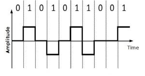
 Line Coding can be classified into ‘four’ important divisions; they are:

  1. Unipolar Line Coding
  2. Polar Line Coding
  3. Bipolar Line Coding
  4. Manchester Line Coding

Again, Unipolar has an important division, which is ‘NRZ’.

Polar has two important divisions; they are ‘NRZ’ & ‘RZ’.

Bipolar is divided into AMI.

Explain each of the Line Coding and their respective divisions:

  • UNIPOLAR In this type of line code method, the signal levels lie above the axis or below the axis.

Diagram:

Manchester code
Image Credit – Original: Dysprosia Derivative work: Nzeemin contribs), Manchester codeCC BY-SA 3.0

In positive logic, unipolar signalling the binary 1 is represented by a high level and a binary 0 by a zero-voltage level. This type of signalling is also called on-off signalling.

NON return to zero (NRZ):

NRZ is a special type of Unipolar coding where the positive voltages denote bit 1 and the zero voltage defines bit 0. Here, the signal does not return to zero hence the name is NRZ.

POLAR

In a polar type of coding, the signal levels lie on the both sides of the axis.

Here, binary 1’s and 0’s are denoted by equal +ve and -ve level. E.g., binary 1 is +A volts and binary 0 is a -A volts.

Non return to zero (NRZ) This NRZ is also kind of similar to the unipolar NRZ, but in case of Polar, NRZ is divided into two divisions i.e. NRZ-L & NRZ-I level.

In NRZ-L level, the bit values are determined by the voltage level. Here, binary 0 refers to logic-level low & bit 1 refers to logic-level high.

In NRZ-I level, when the logic refers to bit 1, two level transition takes place at the boundary & when the logic level refers to 0, no transition occurs at the boundary.

Return to zero (RZ)

unlike NRZ, here the signal value returns to zero. Hence, to Solve some NRZ problems, RZ scheme is applied. RZ uses three values which are a. positive b. negative & c. zero.

A major drawback of RZ is it requires greater bandwidths. Also, since it uses three levels of voltages, this scheme is considered to be a bit complex.

  • BIPOLAR In this type of coding, three different levels of voltages exist; they are positive, negative & zero. In which, one of them lies at zero and the other voltage levels stay at positive and negative.

Diagram:

3

This coding is also called pseudo-ternary signalling or alternative mark inversion (AMI) signalling. In this case, binary 1’s are represented by alternatively positive or negative values. The binary 0 is represented by a zero level.

The term pseudo-ternary means three encoded signal levels (+A, -A and zero volt) are used to represent two level binary data 1 & 0.

Alternative Mark Inversion (AMI)In this scheme, when the voltage is neutral, it refers to binary 0 and when the voltage is positive or negative the binary becomes 1.

Pseudo-ternary  In this coding scheme, bit 1 refers to zero voltage & bit 0 refers to any of positive or negative voltage alternatively.

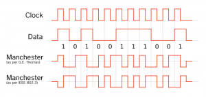
Manchester coding

Here, in this type of coding, symbol 1 is characterized by transmit a +ve pulse (say +A volts) for one-half of the signal length followed by a -ve pulse (say -A volts) for the other half of the signal length.

Correspondingly, symbol ‘0’ is characterized by a -ve half-bit pulse following the +ve half-bit pulse in Manchester encoding techniques.

Diagram:

Manchester encoding
Manchester encoding, Image Credit – Stefan Schmidt, Manchester encoding both conventions, marked as public domain, more details on Wikimedia Commons

Manchester encoding is also called split-phase encoding.

Unlike NRZ or RZ, Manchester Encoding overcomes several issues in between the signals. In this Manchester encoding, there is no baseline wandering; neither there is any DC components as they are consisted with both of positive and negative voltage.

The only drawback of Manchester encoding scheme is its minimum bandwidth requirements.

What is Differential Encoding?

At what time serial-data is carrying through circuits along a communication channel a problem arises. The waveform is likely to be inverted i.e. data complementation takes place. This means 1 may become 0 or 0 may become 1. This may occur in a twisted pair communication channels if a line code like polar signalling is utilized.

To overcome this problem in polar signalling, differential encoding is often used.

In a differential encoder, the encoded differential data are generated by a modulo 2 addition using XOR gate. Thus

 en = dn en-1

In a differential encoding system, the decoded sequence remains same irrespective of the channel polarity.Let us consider the input sequence dn = 1 1 0 1 0 0 1. The encoded sequence due to differential encoding will be en = 1 0 1 1 0 0 0 1.

What are the advantages and disadvantages of Unipolar Line Coding?

Advantages:

  • Unipolar is the simplest type of technique.
  • Always requires less bandwidth.
  • The spectral line can be used here in unipolar RZ as clock

Disadvantages:

  • No clock is present at unipolar NRZ.
  • Signal droop occurs due to low frequency components.
  • Unipolar RZ requires more bandwidth i.e. twice than unipolar NRX.

What are the advantages and disadvantages of Polar Line Coding?

Advantages:

  • This technique is also a simple one.
  • No low frequency components are present

Disadvantages:

  • No presence of clock
  • No checking of errors
  • Polar RZ signal’s bandwidth is twice than the NRZ

What are the advantages of Bipolar Coding?

Advantages:

  • No low frequency components.
  • Single error detection cam be done.
  • It demands lower bandwidth than both of Polar and Unipolar.

Disadvantages:

  • No clock is present
  • Provides less synchronization\\
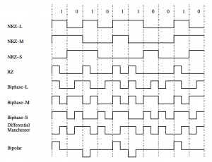
Binary Line Code Waveforms
Various encodings, Image Credit – JugandiBinary Line Code WaveformsCC BY-SA 4.0

For more electronics related articles click here
Maximum Power Transfer Theorem | 3+ Important Steps| Explanations

MPT1 300x203 1

Image Credit: Iñigo Gonzalez from Guadalajara, Spain, Lamp @Ibiza (624601058)CC BY-SA 2.0

Points of Discussion

Introduction to Maximum Power Transfer Theory

In the previous articles related to circuit analysis, we have come across several methods and theories regarding solving problems of a complex network. The maximum power transfer theorem is one of the efficient theories needed to analyze and study advanced circuits. It is one of the primary methods yet important one.

We will discuss the theories, the problem-solving steps, real-world applications, the explanation of the theory. A mathematical problem is solved at last for a better understanding.

Know about: Thevenin’s Theorem! Click Here!

Theory of Maximum Power Transfer Theorem

Maximum power Transfer Theory:

It states that a DC Circuit’s load resistance receives the maximum power if the magnitude of the load resistance is the same as the Thevenin’s equivalent resistance.

The theory is used to calculate the value of load resistance, which causes the maximum power transferred from the source to the load. The theorem is valid for both AC and DC circuits (Point to be noted: For AC circuits, the resistances are replaced by impedance).

Real world Applications of Maximum power transfer theorem

The maximum power transfer theorem is one of the efficient theorems. That is why there are several real-world applications for this theory. The communication sector is one of its fields. The theory is used for low strength signals. Also, for loud speakers to drain the maximum power from the amplifier.

Know about: Norton’s Theorem! Click Here!

Steps for solving problems regarding Maximum Power Transfer Theorem

In general, the below mentioned steps are followed for solving power transfer theory problems. There are other ways, but following these steps will lead to a more efficient path.

  • Step 1: Find out the load resistance of the circuit. Now remove it from the circuit.
  • Step 2: Calculate the Thevenin’s equivalent resistance of the circuit from the open circuited load resistance branch’s view point.
  • Step 3: Now, as the theory says, the new load resistance will be the Thevenin’s equivalent resistance. This is the resistance that is responsible for Maximum power transfer.
  • Step 4: The maximum power is derived then. It comes as follows.

PMAX = VTH2 / 4RTH

Know about: Superposition Theorem! Click Here!

Explanations of the Maximum Power Transfer Theory

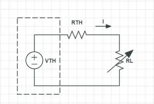
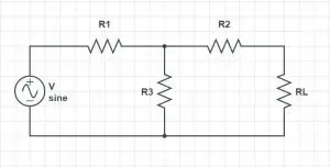
To explain the theorem, let us take a complex network as below.

Maximum Power Transfer Theorem - 1
Example :Thevenin’s equivalent Circuit, Maximum Power Transfer Theorem – 1

In this circuit, we have to calculate the value of load resistance for which the maximum power will be drained from the source to the load.

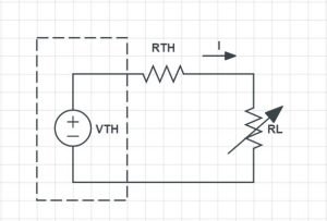
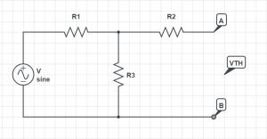
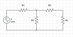
As we can see in the above images, the variable load resistance is attached to the DC circuit. In the second image, the Thevenin’s equivalent circuit is already represented (both the Thevenin’s equivalent circuit and Thevenin’s equivalent resistance).  

From the second image, we can say current (I) through the circuit is:

I = VTH / (RTH + RL)

The power of the circuit is given by P = VI.

Or, P = I2 RL

Substituting the value of I from the Thevenin’s equivalent circuit,

PL = [VTH / (RTH + RL)]2 RL

We can observe that the value of PL can be increased or preferably varied by changing RL‘s value. According to the rule of calculus, the maximum power is achieved when the derivative of the power with respect to the load resistance is equal to zero.

 dPL / dRL = 0.

Differentiating PL, we get,

dPL / dRL = {1 / [(RTH + RL)2]2} * [{(RTH + RL)2 d/dRL (VTH2 RL)} – {(VTH2 RL) d/dRL (RTH + RL)2}]

Or, dPL / dRL = {1 / (RTH + RL)4} * [{(RTH + RL)2 VTH2} – {VTH2 RL * 2 (RTH + RL)

Or, dPL / dRL = [VTH2 * (RTH + RL – 2RL)] / [(RTH + RL)3]

Or, dPL / dRL = [VTH2 * (RTH – RL)] / [(RTH + RL)2]

For the maximum value, dPL / dRL = 0.

So, [VTH2 * (RTH – RL)] / [(RTH + RL)2] = 0

From which, we get,

(RTH – RL) = 0 or, RTH = RL

It is now proved that the maximum power will be drawn when the load resistance and internal equivalent resistance are the same.

So, the maximum power which can be drawn by any circuit,

PMAX = [VTH / (RTH + RL)]2 RL

Now, RL = RTH

OR, PMAX = [VTH / (RTH + RTH)]2 RTH

OR, PMAX = [VTH2 / 4RTH2] RTH

OR, PMAX= VTH2 / 4RTH

This is the power drawn by the load. The power received by the load is the same power send by the load.

So, the total supplied power is:

P = 2 * VTH2 / 4RTH

Or, P = VTH2 / 2RTH

The efficiency of the power transfer is calculated as follows.

η = (PMAX / P) * 100 % = 50 %

This theory aims to gain the maximum power from the source by making the load resistance equal to the source resistances. This idea has different and several applications in the field of communication technology, especially the signal analysis part. The source and load resistances are matched previously and decided before the circuit operation started to attain the maximum power transfer condition. The efficiency comes down to 50%, and the flow of power started from source to load.

Now, for electrical power transmission systems, where the load resistances have higher values than the sources, the condition of maximum power transfer is not achieved easily. Also, the efficiency of the transfer is just 50%, which has no good economical values. That is why the power transfer theorem is rarely used in the power transmission system.

Know about: KCL, KVL Theorems! Click Here!

Problems Related to Maximum Power Transfer Theorem

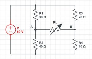
Observe the circuit carefully and calculate the resistance value to receive the maximum power. Apply maximum power transfer theorem to find out the amount of power transferred.

Maximum Power Transfer Theorem - 2
Circuit, Maximum Power Transfer Theorem – 2

Solution: The problem is solved by following the given steps.

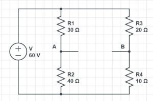
In the first step, the load resistance is disconnected from the circuit. After disconnecting the load, we mark it as AB. In the next step, we will calculate the Thevenin’s equivalent voltage.

Maximum Power Transfer Theorem - 3
The load is removed, Maximum Power Transfer Theorem – 3

So, VAB = VA – VB

VA comes as: VA = V * R2 / (R1 + R2)

Or, VA = 60 * 40 / (30 + 40)

Or, VA = 34.28 v

VB comes as:

VB = V * R4 / (R3 + R4)

Or, VB = 60 * 10 / (10 + 20)

Or, VB = 20 v

So, VAB = VA – VB

Or, VAB = 34.28 – 20 = 14.28 v

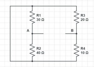
Now, it is time to find out the Thevenin’s equivalent resistance for the circuit.

For that, we short circuit the voltage source and the resistance values are calculated through the open terminal of the load.

RTH = RAB = [{R1R2 / (R1 + R2)} + {R3R4 / (R3 + R4)}]

OR, RTH = [{30 × 40 / (30 + 40)} + {20 × 10 / (20 + 10)}]

OR, RTH = 23.809 ohms

Maximum Power Transfer Theorem - 4
Calculation of resistances, Maximum Power Transfer Theorem – 4

Now the circuit is redrawn using the equivalent values. The maximum power transfer theorem says that to obtain the maximum power, the load resistance = Thevenin’s equivalent resistance. So as per the theory, load resistance RL = RTH = 23.809 ohms.

Maximum Power Transfer Theorem - 5
Final Equivalent Circuit, Maximum Power Transfer Theorem – 5

Formula for the maximum power transfer is PMAX = VTH2 / 4 RTH.

Or, PMAX = 14.282 / (4 × 23.809)

Or, PMAX = 203.9184 / 95.236

Or, PMAX = 2.14 Watts

So, the maximum amount of transferred power is 2.14 watts.

Know about: Circuit Analysis! Click Here!

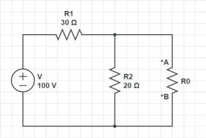
2. Observe the circuit carefully and calculate the resistance value to receive the maximum power. Apply maximum power transfer theorem to find out the amount of power transferred.

Maximum Power Transfer Theorem - 6
Circuit for Problem No. 2, Maximum Power Transfer Theorem – 6

Solution: The problem is solved by following the given steps.

In the first step, the load resistance is disconnected from the circuit. After disconnecting the load, we mark it as AB. In the next step, we will calculate the Thevenin’s equivalent voltage. VTH = V * R2 / (R1 + R2)

VTH = V * R2 / (R1 + R2)

Or, VTH = 100 * 20 / (20 +30)

Or, VTH = 4 V

Now, it is time to find out the Thevenin’s equivalent resistance for the circuit. The resistances are in parallel with each other.

So, RTH = R1 || R2

Or, RTH = 20 || 30

Or, RTH = 20 * 30 / (20 + 30)

Or, RTH = 12 Ohms

Now the circuit is redrawn using the equivalent values. The maximum power transfer theorem says that to obtain the maximum power, the load resistance = Thevenin’s equivalent resistance. So as per the theory, load resistance RL = RTH = 12 ohms.

Formula for the maximum power transfer is PMAX = VTH2 / 4 RTH.

Or, PMAX = 1002 / (4 × 12)

Or, PMAX = 10000 / 48

Or, PMAX = 208.33 Watts

So, the maximum amount of transferred power is 208.33 watts.

Check out Our Latest releases on Electronics Engineering.

.

3 Important Theorems On Electrical Circuit Analysis

TH1 300x152 1

Points of Discussion: Electrical Circuit Analysis

Introduction to Advanced Electrical Circuit Analysis

We came to know the primary circuit structure and some essential terminologies in the previous circuit analysis article. In the DC Circuit analysis, we have studied KCL, KVL. In this article, we are going to learn about some advanced methods for circuit analysis. They are – Superposition theorem, Thevenin’s theorem, Norton’s theorem. There are many more methods for circuit analysis like – maximum power transfer theory, Millman’s theory, etc.

We will learn about the theory of the methods, the detailed explanation of the theory and steps for solving circuit problems.

Basic Terminologies Related to Circuit Analysis : Click Here!

Advanced Electrical Circuit Analysis: Thevenin’s Theorem

Thevenin’s theorem (Helmholtz – Thevenin theorem) is one of the most crucial theories needed for analysing and studying complex circuits. It is one of the simplest methods to solve complex network problems. Also, it is one of the most widely used methods for circuit analysis.

Thevenin’s Theorem: It states that all complex networks can be replaced by a voltage source and a resistance in series connection.

In simpler words, if a circuit has energy sources like dependent or independent voltage sources, and has a complex structure of resistances, then the whole circuit is representable as a circuit consisting the equivalent voltage source, the load resistance, and the equivalent resistance of the circuit, all in series connection.

Steps for solving problems regarding Thevenin’s theorem

  • Step 1: Remove the Load Resistance and redraw the circuit. (Note: The load resistance will be the referenced resistance through which you have to calculate the current).
  • Step 2: Find out the open circuit voltage or Thevenin’s equivalent voltage for the circuit.
  • Step 3: Now short circuit all the voltage sources, and open circuit all the current sources. Also, substitute all the elements with their equivalent resistances and redraw the circuit (Note: Keep the load resistance is unattached).
  • Step 4: Find out the equivalent resistance of the circuit.
  • Step 5: Draw a fresh circuit with a voltage source and two resistance in series with it. The magnitude of the voltage source will be the same as the derived equivalent Thevenin’s voltage. One of the resistances will be the pre-calculated equivalent resistance, and the other is the load resistance.
  • Step 6: Calculate the current through the circuit. That is the final answer.

Explanation

To explain the theorem, let us take a complex circuit as below.

Electrical circuit analysis
Example Circuit, Electrical Circuit Analysis – 1

In this circuit, we have to find out the current I, through the resistance RL using the Thevenin’s theorem.

Now, to do so, first remove the load resistance and make that branch open circuited. Find out the open circuit voltage or Thevenin’s equivalent across that branch. The open circuited voltage comes as: VOC = I R3 = (VS / R1 + R3) R3

TH2
The Load is removed, Electrical Circuit Analysis – 2

For calculation of the equivalent resistance, the voltage source is short circuited (deactivated). Now, find out the resistance. The equivalent resistance comes out as: RTH = R2 + [(R1 R3) / (R1 + R3)]

TH3
The voltage source is short circuited & the equivalent resistance is calculated, Electrical Circuit Analysis – 3

At the last step, make a circuit using the derived equivalent voltage and equivalent resistance. Connect the load resistance in series with the equivalent resistance. 

The current comes as: IL = VTH / (RTH + RL)

TH4
Thevenin’s Equivalent Circuit, Electrical circuit Analysis – 4

Electrical Circuit Analysis: Norton’s Theorem

Norton’s theorem (Mayer – Norton Theorem) is another crucial theory needed to analyses and study complex circuits. It is one of the simplest methods to solve complex network problems. Also, it is one of the most widely used methods for circuit analysis.

Norton’s Theorem: It states that all complex networks can be replaced by a current source and a resistance in parallel connection.

In simpler words, if a circuit has energy sources like dependent or independent current sources, and has a complex structure of resistances, then the whole circuit is representable as a circuit consisting the equivalent current source, the load resistance, and the equivalent resistance of the circuit, all in parallel connection.

Steps for solving problems regarding Norton’s theorem

  • Step 1: Short circuit the Load Resistance and redraw the circuit. (Note: The load resistance will be the referenced resistance through which you have to calculate the current).
  • Step 2: Find out the short circuit current or Norton’s current of the circuit.
  • Step 3: Now, short circuit all the independent sources. Also, substitute all the elements with their equivalent resistances and redraw the circuit (Note: Make the load resistance unattached).
  • Step 4: Find out the equivalent resistance of the circuit.
  • Step 5: Draw a fresh circuit with a current source and two resistance in parallel with it. The magnitude of the current source will be the same as the derived equivalent short-circuit current. One of the resistances will be the pre-calculated equivalent resistance, and the other is the load resistance.
  • Step 6: Calculate the current through the circuit. That is the final answer.

Explanation

To explain the theorem, let us take a complex circuit as below.

TH1 1
Example Circuit, Electrical Circuit Analysis – 5

In this circuit, we have to find out the current I, through the resistance RL using Norton’s theorem.

To do so, first, remove the load resistance (RL) and make that branch short circuited. The current in the closed loop is calculated first.

I = VS / [ R1 + {R2R3/ (R2 + R3)}]

The short circuit current comes as ISC = I R3 / (R3 + R2)

NT2
Load is removed and short circuited, Electrical circuit analysis – 6

The voltage source is short circuited (deactivated) and the load resistance branch is short circuited for calculation of the equivalent resistance. Now, find out the resistance. The equivalent resistance comes out as: RNT = R2 + [(R1 R3) / (R1 + R3)]

NT3
Equivalent Resistances, Electrical circuit analysis – 7

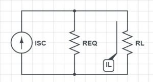
At the last step, make a circuit using the derived equivalent current source and equivalent resistance. Connect the load resistance in parallel with the equivalent resistance and the current source in parallel with them. 

The current comes as: IL = ISC RNT / (RNT + RL)

NT4
Norton’s Equivalent Circuit, Electrical circuit Analysis – 8

Electrical Circuit Analysis: Superposition Theorem

Superposition theorem is another crucial theory needed for analysing and studying of complex circuits. It is another easy method to solve complex network problems. Also, it is one of the most widely used methods for circuit analysis. Superposition theory is only applicable for linear circuits and circuits which obey Ohm’s law.

Superposition Theorem: It states that for all active, linear circuits, which have multiple sources, the response across any circuit element, is the aggregate sum of the responses obtained from each source considered separately and every source are substituted by their internal resistances.

In a more general way, the theorem states that the aggregate current in each branch can be expressed as the sum of all currents produced for a linear network. At the same time, all the source acted separately, and their internal resistances substitute independent sources.

Steps for solving problems regarding superposition theorem

  • Step 1: Consider one independent source at a time and deactivate (short-circuit) all the other sources.
  • Step 2:  Replace that other source with the equivalence of the resistors of the circuits. (Note: By default, if the resistance is not given, make it short-circuit).
  • Step 3: Now, short circuit all the other (leave the selected source) voltage source and open circuit all the other current source. 
  • Step 4: Find the current for every branch of the circuit.
  • Step 5: Now choose another voltage source and follow step 1-4. Please do it for every independent source.
  • Step 6: At last, calculate the current for each branch by superposition theorem (addition). To do so, add up currents of the same branch calculated for different voltage sources. Add the direction of the currents wise (if the same direction – add up, else minus).

Explanation

To explain the method, let us take a complex circuit as below.

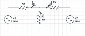
SP1
Superposition Theorem Circuit, Electrical circuit Analysis – 9

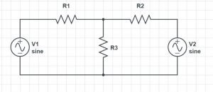
In this circuit, we have to find out the current through each branch. The circuit has two voltage sources.

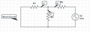
At first, we choose the V1 source. So, we short circuit (as the source’s internal resistance is not given) the other voltage source – V2.

SP2 1
One source is removed, Electrical circuit Analysis – 10

Now, calculate all the current for every branch. Let the current through the branches are – I1`, I2`, I3`. They are represented as follow.

I1` = V1 / [ R1 + {R2R3/ (R2 + R3)}]

I2` = I1` R3 / (R3 + R2)

Now, I3` = I1` – I2`

The V2 voltage source is activated in the next step while the V1 source is deactivated or short circuited (internal resistance is not given).

SP3
Another Source is removed, Electrical circuit Analysis – 11

As the previous step, here we need to calculate the current for every branch again. The current through the branches comes as follow.

I2“ = V2 / [ R2 + {R1R3/ (R1 + R3)}]

I1“ = I2“ R3 / (R3 + R1)

Now, I3“ = I2“ – I1

SP5
Current in the branches, Electrical circuit Analysis – 12

All the source calculation is now covered. Now, we have to apply superposition theorem and find out the net currents for the branches. The direction rule is considered while calculating. The I1, I2, I3 magnitudes are given below.

I3 = I3` + I3

I2 = I2` – I2

I1 = I1` – I1

For mathematical problems, check out the next article.

AC Circuit Analysis: 3 Important Facts You Should Know

RC Series 300x159 1

Points of Discussions: AC Circuit Analysis

Introduction to Advanced AC Circuit Analysis

In the previous article of the AC circuit, we have discussed some of the basic ac circuit analysis. We have studied about the circuit, the phasor diagrams, power calculations, and some essential terminologies. In this article, we will learn some advanced AC circuit analysis like – RC Series circuit, RL series circuit, RLC series circuit, etc. These advanced circuits are essential and have more applications in electrical analysis. All of these circuits can be said another level of primary ac circuit as the more complex circuit can be built using these. Please check out the introductory circuit article before studying this advanced ac circuit analysis.

Basic AC Circuit Analysis: Read Here!

RC Series Circuit

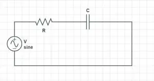
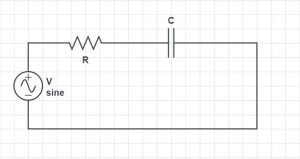
If a pure resistor is placed in a series with a pure capacitor in an AC circuit, then the ac circuit will be called RC AC Series Circuit. An ac voltage source produces sinusoidal voltages and the current passes through the resistor and the capacitor of the circuit.

  • Circuit diagram of RC series circuit
RC Series Circuit, AC circuit analysis
RC Series Circuit, AC Circuit analysis – 1

VR gives the voltage across the resistance, and – VC gives the voltage across the capacitor. The current through the circuit is I. R is the resistance and C is the capacitance value. XC denotes the capacitive reactance of the capacitor.

Widerstand ZeigerRC 1
phasor diagram of RC series Circuit, Ac circuit analysis – 2, Image Credit – Saure at German WikipediaWiderstand ZeigerRCCC BY-SA 3.0

The process to draw the phasor diagram of RC Circuit.

The phasor diagram is an essential analytical tool which helps to study the behaviour of the circuit. Let us learn the steps to draw the phasor.

Step 1. Find out the r.m.s value of the current. Mark that as the reference vector.

Step 2. As we know that for a purely resistive circuit, voltage and current remains in the same phase, here as well voltage drop across the resistor stays in phase with the current value. It is given as V = IR.

Step 3. Now for the capacitive circuit, we know that voltage lags by 90 degrees and current leads. That is why voltage drop across the capacitor in this circuit, stays 90 degrees behind than the current vector.

Step 4. The applied voltage thus comes as the vector sum of the voltage drops of capacitor and resistances. So, it can be written as:

V2 = VR2 + VC2

Or, V2 = (IR)2 + (IXC)2

Or, V = I √ (R2 + XC2)

Or, I = V / √ (R2 + XC2)

Or, I = V / Z

Z is the aggregate impedance of the RC circuit. The following equation represents the mathematical form.

Z = √ (R2 + XC2)

Now from the phasor diagram, we can observe there is an angle as – ϕ.

So, tan ϕ will be equal to IXC / IR.

So, ϕ = tan-1 (IXC / IR)

This angle ϕ is known as phase angle.

  • RC Series Circuit Power calculation

The power of the circuit is calculated by P = VI formula. Here we will calculate the instantaneous value of power.

So, P = VI

Or, P = (Vm Sinωt) * [Im Sin (ωt+ ϕ)]

Or, P = (Vm Im / 2) [ 2Sinωt * Sin (ωt+ ϕ)]

Or, P = (Vm Im / 2) [ cos {ωt – (ωt+ ϕ)} – cos {ωt – (ωt+ ϕ)}]

Or, P = (Vm Im / 2) [ cos (- ϕ) – cos (2ωt+ ϕ)]

Or, P = (Vm Im / 2) [ cos (ϕ) – cos (2ωt+ ϕ)]

Or, P = (Vm Im / 2) cos (ϕ) – (Vm Im / 2) cos (2ωt+ ϕ)

We can observe that the power equation has two sections. One is a constant part another is the variable section. The mean of the variable part comes to be zero over a full cycle.

So, the average power for an RC series circuit, over a full cycle is given as :

P = (Vm Im / 2) cos (ϕ)

Or, P = (Vm / √2) * (Im / √2) * cos (ϕ)

Or, P = VI cos (ϕ)

Here, V and I are considered as RMS values.

The power factor of RC Series Circuit

The RC series circuit’s power factor is given by the ratio of active power to the apparent power. It is represented by cosϕ and expressed as below given expression.

cos ϕ = P / S = R / (R2 + XC2)

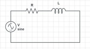
RL Series Circuit

If a pure resistor is placed in a series with a pure inductor in an AC circuit, then the ac circuit will be called RL AC Series Circuit. An ac voltage source produces sinusoidal voltages and the current passes through the resistor and the inductor of the circuit.

  • Circuit Diagram of RL circuit
RL
RL Series Circuit, AC Circuit analysis – 3

VR gives the voltage across the resistance, and – VL gives the voltage across the inductor. The current through the circuit is I. R is the resistance and L is the inductance value. XL denotes the inductive reactance of the inductor.

  • Phasor Diagram of RL circuit
RL IU Zeiger
RL Circuit Phasor Diagram, AC Circuit Analysis – 4, Image Credit – SaureRL I(U)-ZeigerCC BY-SA 3.0

The process to draw the phasor diagram of RL Circuit.

Step 1. Find out the r.m.s value of the current. Mark that as the reference vector.

Step 2. As we know, for a purely resistive circuit, voltage and current remain in the same phase, here as well voltage drop across the resistor stays in phase with the current value. It is given as V = IR.

Step 3. Now for the inductive circuit, we know that voltage leads by 90 degrees and the current lags. That is why voltage drop across the inductor in this circuit, stays 90 degrees ahead than the current vector.

Step 4. The applied voltage comes as the vector sum of the voltage drops of inductor and resistances. So, it can be written as:

V2 = VR2 + VL2

Or, V2 = (IR)2 + (IXL)2

Or, V = I √ (R2 + XL2)

Or, I = V / √ (R2 + XL2)

Or, I = V / Z

Z is the aggregate impedance of the RL circuit. The following equation represents the mathematical form.

Z = √ (R2 + XL2)

Now from the phasor diagram, we can observe there is an angle as – ϕ.

So, tan ϕ will be equal to IXL / IR.

So, ϕ = tan-1 (XL / R)

This angle ϕ is known as phase angle.

  • RL Series Circuit Power calculation

The power of the circuit is calculated by P = VI formula. Here we will calculate the instantaneous value of power.

So, P = VI

Or, P = (Vm Sinωt) * [Im Sin (ωt- ϕ)]

Or, P = (Vm Im / 2) [ 2Sinωt * Sin (ωt – ϕ)]

Or, P = (Vm Im / 2) [ cos {ωt – (ωt – ϕ)} – cos {ωt – (ωt – ϕ)}]

Or, P = (Vm Im / 2) [ cos (ϕ) – cos (2ωt – ϕ)]

Or, P = (Vm Im / 2) cos (ϕ) – (Vm Im / 2) cos (2ωt – ϕ)

We can observe that the power equation has two sections. One is a constant part another is the variable section. The mean of the variable part comes to be zero over a full cycle.

So, the average power for an RL series circuit, over a full cycle is given as :

P = (Vm Im / 2) cos (ϕ)

Or, P = (Vm / √2) * (Im / √2) * cos (ϕ)

Or, P = VI cos (ϕ)

Here, V and I are considered as RMS values.

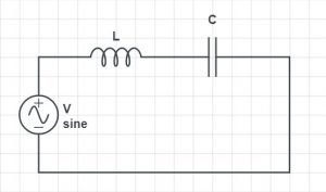
LC Series Circuit

An LC series circuit is an AC circuit consisting of inductor and capacitor, placed in a series connection. An LC circuit has several applications. It is also known as a resonant circuit, tuned circuit, LC filters. As there is no resistor in the circuit, ideally this circuit doesn’t suffer any losses.  

LC Circuit as Tuned Circuit: The flow of current means flows of charges. Now in an LC circuit, charges keep flowing behind and ahead of the capacitor plates and through the inductor. Thus, a type of oscillation gets created. That is why these circuits are known as tuned or tank circuit. However, the internal resistance of the circuit prevents the oscillation in real.

  • Circuit diagram of LC Series Circuit
LC
Series LC Circuit, Tank circuit, Ac Circuit Analysis

In a series circuit, the current value is the same across the whole circuit. So we can write that, I = IL = IC.

The voltage can be written as V = VC + VL.

  • Resonance in series LC Circuit

Resonance is refereed to as a particular condition of this LC circuit. If the frequency of the current increases, the value of inductive reactance also gets increased, and the value of capacitive reactance gets decreased.

XL = ωL = 2πfL

XC = 1 / ωC = 2πfC

At the resonance condition, the magnitude of capacitive reactance and inductive reactance is equal. So, we can write that XL = XC

Or, ωL = 1 / ωC

Or, ω2C = 1 / LC

Or, ω = ω0 = 1 / √LC

Or, 2πf = ω0 = 1 / √LC

Or, f0 = ω0 / 2π = (1/2π) (1 / √LC)

f0 is the resonant frequency.

  • The impedance of the circuit

Z = ZL + ZC

Or, Z = jωL + 1 / jωC

Or, Z = jωL + j / j2ωC

Or, Z = jωL – j / ωC

Sampling Theorem & Encoding in Digital Communication:7 Facts

advisor answer answers assistance 1 300x225 1

Topic of Discussion: Digital Communication

  • Introduction to Digital Communication
  • It’s advantages over Analog communication
  • What is Encoding
  • Types of Encoding
  • Companding in Encoding
  • Sampling Theorem

To know about encoding and other features, first, we have to recall what digital communication is and some of its advantages.

What is Digital Communication?

Definition & the advantages of Digital communication:

It is the type of communication system, in which the signals which are used to transmit data or information, should be discrete in time & amplitude. They are also called digital signals

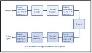
comunication 1
Digital Communication system

Some of the important advantages are:

  • Digital communications provide increased immunity to noise and external interference.
  • It offers better flexibility and compatibility.
  • Digital communication gives improved reliability due to channel coding.
  • Digital Communication system is comparatively simpler and cheaper than an analog communication system.
  • Computers can be used directly for digital signal processing.
  • It makes communication more secured using data encryption.
  • Wideband channels are available for digital communications.

What is Encoding?

advisor answer answers assistance 1
Encoding in digital communication

Introduction to encoding in digital communication:

Encoding is a special type of process in which various patterns or voltages or current levels are used to represent 1s and 0s of the digital signals on a particular transmission link or channel.

What are the different types of encoding?

There are four types of encoding; they are-

  • Unipolar
  • Polar
  • Bipolar
  • Manchester

What is Companding?

Why is Companding needed in encoding?

Quantization is of two types

  • Uniform Quantization,
  • Non-Uniform Quantization.

Non-Uniform quantization is achieved through companding. This is a process in which compression of the input signal is done in the transmitter, whereas the expansion of the signal is done at the receiver. The combination of compressing and expanding is companding.

The process of Companding:

In a linear or uniform quantization, the small amplitude signals would have a poor SNR than the large-amplitude signals. This is a drawback of linear quantization. To remove this problem, non-uniform quantization is utilized in which the step size differs with the amplitude of the i/p. The step size variation is achieved by distorting the input signal before the quantization process. This process of distorting the input signal before quantization is known as compression, in which the signal is amplified at low signal level and attenuated at high signal level.

After compression, uniform quantization is applied. Here the signal is companding, which is to make the overall transmission distortion less.

Input Output characteristics of a Compander:

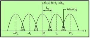
What is Aliasing?

Define the Aliasing Effect:

  • Aliasing is an important term in encoding & digital communication itself.
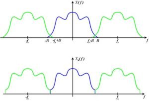
  • If signal is sampled at a rate lesser than the Nyquist Rate, the side band overlap, producing an interference-effect. This is called the Aliasing Effect.
  • If aliasing takes place, it is not possible to recover the original analog signal.
aliasing
Aliasing Effect

Anti-Aliasing Filter:

To remove the problem of the aliasing from the signals, a special type of filter is used, which is known as the Anti- Aliasing Filter.

An anti-aliasing filter is usually at the input of a PAM generator to avoid the effect of aliasing. PAM signal is generated by sampling the input analog signal in a sampler circuit.

The sampling is thru in accord with the Sampling Theorem , i.e., the sampling frequency fs is kept equal to or higher than twice the maximum frequency W present in the input analog signal. If, however, fs<2W, then aliasing occurs, and recovery of the original analog signal will not be possible. Since fs is usually kept unchanged, the input analog signal is passed through a low pass filter before sampling to band limit the analog signal in conformity with the sampling theorem.

What is Sampling?

State Sampling Theorem:

The mathematical basis of the sampling process has been laid by the Nyquist sampling theorem. It also gives an idea about the recovery of the original signal completely from its samples. The statement of the sampling theorem is thus given in two parts below’;

  • A band-limiting signal of finite energy that has no freq. rage of W Hz is usualy designated by agreeing the value of the signals at that time parted by ½ W sec.
  • A band-limit signal of finite energy that has no freq. components outside the W Hz might be totally reformed from the information of its sample data rated @2W sample/sec.

The sampling rate 2W/sec is entitled as the “Nyquist Rate.” in the Sampling Theorem explanation.

The reciprocal 1/2W is entitled “Nyquist Interval.”

Nyquist Shannon sampling theorem
Nyquist–Shannon sampling theorem, Image Credit – anonymous, AliasedSpectrum, marked as public domain, more details on Wikimedia Commons

How does sampling theorem work in encoding?

In sampling theorem, the received message (baseband) signals are sampled with a typical combination of rectangular-shaped or square-shaped pulses. For the accurate reconstruction of the message signal in the receiving end, the sampling rate has to be more than double of maximum freq. component specified by ‘W’. In a practical case, an anti-aliasing filter (lpf) is utilized at the sampler device to discard the frequencies band those are greater than the W. Hence, the various utilization of sampling allows the minimization of the incessantly changeable message signal (of some determinate period) to some degree of discrete quantity per sec.

Explain the Encoding Process:

In merging the sampling theorem and quantization procedures, the order of a continuous message (baseband) signal converts limited to discrete values but not in the procedure appropriate for the transmission over a long-distanced radio telecommunication channel. To utilize the benefits of sampling and quantization to create the communicated signal stronger to noise, interference, and other channel dreadful conditions. The main requirement is an encoding process to interpret the discrete set of sample values to a proper form of signal. This distinct procedure in a code is called a code element or symbol. Specific prearrangement of symbols employed in coding to signify a single value of the distinctive set is entitled as ‘codeword’ or ‘character’.

In binary encryption, the symbol is in two distinctive values, such as a -ve pulse or a +ve pulse. The binary codes are, as a matter of course, signified as 0 and 1 combination only.

Actually, a binary code is favored over other codes such as ternary cod for the following grounds.

  • The more significant advantages over the effects of noise in a transmission channel could be obtained using a binary code because of its sustainability with higher noises.
  • Another reason is the binary code is comparatively simplified to produce and to regenerate again.

What is A-law and μ-law in companding?

There are two types of compression laws in use. These are, namely, ? law & A-law companding.

? law companding is used in various country A-law companding recommended by CCITT is used in asian and European countries.

? law is defined by the expression-

The A-law compression characteristic is finished up of a linear segment for low-level input and a log-segment for higher level input. The special case A=1 corresponds to uniform quantization. A applied value for A is 87.561.

A-law companding is inferior to ? law in terms of small-signal quality, i.e., ideal channel noise.

For more related topics and MCQ click here

Encoding In Communication,Probability & Random Process:33 QA

1. Sampling theorem is mostly used in

  1. Amplitude modulation (AM)
  2. Frequency modulation (FM)
  3. PCM
  4. none of these

 Answer – (3)

2. What is effective to decrease cumulative error?

  1. PCM
  2. DPCM
  3. Delta Sigma Modulation
  4. ADM

 Answer – (2)

3. What is the Nyquist rate for x(t) = 8cos200πt to remove aliasing effect?

  1. 50Hz
  2. 100Hz
  3. 200Hz
  4. 400Hz

 Answer – (3)

4. How many bits are in need to characterize a 256-level quantization in Pulse Code Modulation ?

  1. 7
  2. 5
  3. 6
  4. 8

 Answer – (4)


5. In Pulse Code Modulation, the amplitude level is transmitted in a 7-units channel code. The sampling is thru at the rate of 10 KHz. The least BW

  1. 5 KHz
  2. 36 KHz
  3. 70 KHz
  4. 85 KHz

 Answer – (2)

6. In Pulse Code Modulation use Lpf

  1. remove aliasing effect
  2. remove quantization noise
  3. remove decoding noise
  4. none of these

 Answer – (1)

7. Adaptive Delta Modulation >> delta modulation as

  1. provides better noise performance
  2. it utilize less number bits used for encoding in communication
  3. it doesn’t suffer from slope overload and threshold effects
  4. simple circuit architecture

 Answer – (3)

comunication

8. The compander in a telecom system is utilized for

  1. equalizing the SNR for both weak and strong PAM signals
  2. increasing amplification of the signals
  3. improving A/D conversion
  4. improving multiplexing

 Answer – (3)

9. Using non-uniform quantization leads to

  1. decrease of transmission band-width
  2. increase in maximum Signal to Noise Ratio
  3. increase in Signal to Noise Ratio for low band signals
  4. Generalization of quantization method

 Answer – (3)

10. What should be the Nyquist sampling rate for the signal s(t) = 10cos (50πt)cos2(150πt) when t is in seconds?

  1. 150 samples/second
  2. 200 samples/second
  3. 300 samples/second
  4. 350 samples/second

 Answer – (4)

11. In a Pulse Code Modulation system, the number of bits (per sample) is increased from n to n+1, the enhancement in Signal to Noise Ratio will be

  1. 3 dB
  2. 6 dB
  3. 2n dB
  4. n dB

 Answer – (2)

12. We detect a PAM signal by using

  1. an ADC
  2. an integrator
  3. a bandpass filter
  4. a high pass filter

Answer – (2)

13. What is the no of bits capable to characterize a 256-level quantization in Pulse Code Modulation?

  1. 7
  2. 8
  3. 5
  4. 6

 Answer – (2)

14. The key advantage of Pulse Code Modulation are

  1. possibility of TDM
  2. less channel bandwidth
  3. less transmission powers
  4. better noise performance

Answer – (4)

15. Regenerative repeater could be utilized in

  1. Analog communication
  2. Digital communication
  3. Both
  4. None of these

Answer – (2)

16. In digital communication, Companding is used to

  1. Reduce the probability of errors
  2. Reduce quantization noise
  3. To increase signal strength
  4. Improve signal to noise ratio for low level input signals

 Answer – (4)

17. The granular noise ensues in the Delta Modulation when the modulating signal

  1. When the modulating signal increases rapidly
  2. When the modulating signal changes with the step size
  3. When the modulating signal decreases rapidly
  4. When the modulating signal has high frequency component

Answer – (2)

18. In which modulation technique, redundant bits should be reduced

  1. ADM
  2. DPCM
  3. PCM
  4. none of these

Answer – (2)

19.  In a Pulse Code Modulation, the no of quantization level is equal to sixteen and 4 kHz is maximum signal frequency. What is the bit transmission rate?

  1. 64 kbps
  2. 32 kbps
  3. 16 kbps
  4. 8 kbps

 Answer – (3)

20. Flat top sampling refers to

  1. an aperture effects
  2. aliasing
  3. loss of the signal
  4. none of these

 Answer – (1)

21. In the present day standard digital voice communication, the amplitude of the voice signal is sampled at a rate of around

  1. 2000 samples/sec
  2. 800 samples/sec
  3. 16000 samples/sec
  4. 8000 samples/sec

 Answer – (4)

22. Choose the right option which is digital in nature

  1. PAM
  2. PPM
  3. DM
  4. none of these

Answer – (4)

23. Pulse suffering is used in

  1. Synchronous TDM
  2. Asynchronous TDM
  3. Any TDM
  4. none of these

 Answer – (2)

  24. The key benefit of Time Division Multiplexing over Frequency Division Multiplexing is that it

  1. needs less power
  2. needs less bandwidth
  3. needs simple circuitry
  4. gives better S/N ratio

Answer – (3)

25. The SNR in PCM system is reliable on

  1. sampling rate
  2. number of quantization levels
  3. message signal bandwidth
  4. none of these

 Answer – (2)

26. A random variable is computed by no. of independent events having Gaussian probability distribution. It is

  1. central limit theorem
  2. superposition
  3. convolution
  4. correlation

 Answer – (1)

27. The probability density function of the envelope of narrowband Gaussian noise is

  1. Poisson
  2. Gaussian
  3. Rayleigh
  4. Rician

Answer – (3)

28. Random process termed “ Ergodic” when

  1. All Ensemble average is not variable
  2. All Ensemble average is constant
  3. All Ensemble average is substitutable

 Answer – (2)

29. A box having four white and three black color balls. Three balls are drawn from the box in succession. Compute the probability that the first two balls are white and the third one is black

  1. 6/35
  2. 4/35
  3. 3/35
  4. 7/35

 Answer – (1)

30. The power spectral density of white noise

  1. Keeps changing as square root of frequency
  2. Keeps changing as inverse of frequency
  3. changes as square of frequency
  4. stays constant with frequency

 Answer – (4)

31. Two dice are thrown simultaneously. The probability of receiving number “5” is?

  1. 1/9
  2. 1/12
  3. 1/36

 Answer – (4)

32. The spectral density plot of white noise will be

  1. Exponential
  2. Uniform
  3. Poisson
  4. Gaussian

 Answer – (2)

33. A rectangular pulse of duration T is used in a matched filter circuit. The output of filter is a

  1. Rectangular pulse of duration T
  2. Rectangular pulse of duration 2T
  3. triangular pulse
  4. impulse function

Answer – (3)

Encoding in communication
Codes used in Encoding in communication, Image Credit – JugandiBinary Line Code WaveformsCC BY-SA 4.0

To learn more on Encoding and other electronic topics click here

Circuit Analysis: 5 Complete Quick Facts

1280px Resistor symbol America.svg 300x113 1

Cover Image Credit – Santeri Viinamäki, MCB Circuit breakers for DIN railCC BY-SA 4.0

Points of discussion : Circuit Analysis

Introduction to Circuit Analysis

Circuit analysis is one of the primary and essential modules for Electrical and Electronics Engineering. Before exploring out the concepts and theories of circuit analysis, let us know what a circuit is.

A circuit can be defined as a closed or open loop consists of electrical and electronic components and have interconnection between them. Circuit analysis is the method to determine the necessary current or voltage value at any point of the circuit by studying and analysing the circuit. There are numerous different methods for circuit analysis and used as per suitable conditions.

What is a DC Circuit? Learn About KCL & KVLs! Click Here!

Ideal Circuit Elements

An ideal circuit can be defined as a circuit without any losses, thus the appearance of 100% input power at the output side. An ideal circuit consists of three ideal elements. They are – Resistances, capacitor, Inductor.

  • Resistors: Resistors are passive electrical components used to resist the flow of electrons in a circuit. The voltage across the resistor is expressed by a famous law, known as Ohm’s law. It states that “the voltages are directly proportional to the currents”. If V and I respectively denote the voltage value and current, then

V ∝ I

Or, V = IR

Here R represents the resistance or resistor value. The unit is given by ohm(Ω).  The following image

represents the resistor –

Resistor Symbol, Circuit analysis image - 1
Resistor Symbol, Circuit analysis image – 1

The following mathematical expression gives the power stored by a resistor.

P = VI

Or, P = (IR) I

Or, P = I2R

Or, P = V2 / R

  • Capacitor: A typical capacitor is a passive electrical equipment which stores electrical energy inside an electric field. It is a two-terminal device. Capacitance is known as the effect of the capacitor. Capacitance has a unit – Farad(F). The capacitor is represented in the circuit by the following image.
1120px Capacitor Symbol.svg
Capacitor Symbol, Circuit Analysis, Image – 2

The relation between charges and capacitance is given by Q = CV, where C is the capacitance value, Q is the Charge, V is the applied voltage.

The current relationship can be derived from the above equation. Let us differentiate both side with respect to time.

dQ/dt = C dV/dt; C is a constant value

Or, I = C dV/dt; as I = dQ/dt.

Power stored in a capacitor can be described written as

P = VI

Or, P = V C dV/dt

Now, the energy is given as U = ∫ p dt

Or, U = ∫ V C (dV/dt) dt

Or, U = C ∫ V dV

If we assume that the capacitor was discharged at the beginning of the circuit, then the power comes as U = ½ CV2.

  • Inductor: Inductor is another passive device present in an ideal circuit. It holds energies in a magnetic field. The unit of inductance is given by Henry(H). The relation between voltage and inductance is given below.

V = L dI/dt

The reserved energies are returned back to the circuitry in current form. The following image represents the inductor in the circuit.

1280px Inductor symbol.svg
Inductor Symbol, Circuit Analysis, image – 3

The power of an inductor is given as P =VI.

Or, P = I * L (dI/dt)

Again, the energy U = ∫ p dt

Or, U = ∫ I * L (dI/dt) dt

Or, U = L ∫ I dI

The energy comes as U = ½ LI2.

Learn about different types of AC Circuits! Click here!

Realistic Circuit Elements

Ideal circuit components are for ideal circuits. They are not applicable in real circuits. However, the main characteristics remain the same for the elements. Elements suffer some loss, have some tolerance values and some abstractions while using it.

The working principles and equations get changed in real domains. Also, some other factors get added during operations. For example, capacitors work differently in high-frequency domains; resistors generate a magnetic field during operations.

  • Resistors: The real-world resistors should be made to obey Ohm’s law as close as they can. The resistance offered by a resistor depends upon the material and shape of the resistor.

A real resistor maybe gets destroyed or burned out due to heat generated by itself. There is a certain tolerance level mentioned for every resistor via the color codes.

  • Capacitors: The realistic capacitors should be made to obey the capacitor’s equation as close as possible. Two conducting surfaces are needed to build a capacitor. They are placed together, and air or any material is filled in between them. The capacitor value is dependent on the surface area of the conductor and the distance between them and upon the permittivity of the inside material. There are various categories of capacitors in the market. Some of them are – Electrolytic Capacitors, Tantalum Capacitors, etc.

Capacitors are connected with wire at their terminals. That causes resistance and a small amount of impedance. An increase in voltage across the capacitors sometimes damages the insulative materials between the plates.

  • Inductors: The realistic or real-world inductors should be made to obey the inductor equation as close as possible. Inductors are choke of coils. They induce magnetic fields to store electrical-energies.

Inductors are made using the winding wires in a coil-like structure: the more the winding, the stronger the magnetic field. Placing a magnetic material inside the coil would increase the magnetic effect. Now, as these wires are wounded around the material, this causes the generation of resistance. Also, it is needed to be large enough to accumulate the magnetic field. That sometimes causes problems.

Ideal Energy Sources

An ideal circuit needs an ideal source of energy. There are two types of ideal energy sources. They are – ideal voltage source and ideal current source.

Ideal Voltage Source: Ideal voltage sources supply a constant amount of voltage for every instant of time. Voltage is constant throughout the source. In reality, there is no ideal source for circuits. It is an assumption to simplify the circuit analysis. The below image represents an ideal voltage source.

Ideal voltage source symbols
Three symbols for ideal voltage source, Circuit analysis image – 4, Image credit – Hardman FeidlimidIdeal voltage source symbolsCC BY-SA 4.0

Ideal Current Source: Ideal current sources supply currents independent of the variation of voltage in the circuit. An ideal current source is an approximation that does not take place in reality but can be achieved. The below picture represents the ideal current source in a circuit.

1024px Current Source.svg
Ideal Current source, Circuit analysis, image – 5

Real energy sources for circuits

Real electrical or electronic circuits need natural sources of energy. There are some differences between ideal and real-world energy sources though the main principle of supplying the energy to the circuit remains the same. Real-world energy sources have several types. Some are even dependent upon other sources. Like – Voltage controlled current source, Current controlled current source, etc. We will discuss them briefly in this circuit analysis article.

  • Voltage Sources: Real voltage sources come up with an internal resistance, which is consider it to be in series with the voltage source. No matter how negligible the resistance is, it affects the V-I characteristic of the circuit. The voltage source can be of two types –
  1. Independent Voltage Source
  2. Dependent Voltage Source

Independent Voltage Sources: These voltage sources have no dependency upon any other energy sources of the circuit. It provides a small resistance, which changes the V-I characteristic plot.

Dependent Voltage Sources: These voltage sources are dependent upon any other energy sources present in the circuits. They can be classified into two categories

  • Voltage Controlled Voltage Source
  • Current Controlled Voltage Source.
  • Voltage Controlled Voltage Source: If any other voltage source is controlled by any kind of voltage source, it is known as Voltage controlled voltage source. V0 = AVc gives voltage output; Here, A represents the gain, and Vc is the controlling voltage.
  • Current Controlled Voltage Source: If any other voltage source is controlled by different current source in the circuit, it is known as a current-controlled current source. V0 = AIc gives the output; Here, A represents the gain, and Ic controls the current.
  • Current Sources: Real current sources come up with internal resistance. The resistance may be negligible but has its effect throughout the circuit. Current Source can be of two kind.
  1. Dependent Source
  2. Independent Source

Independent Source: These current sources have no dependency upon any other energy sources of the circuit. It provides a small resistance, which changes the V-I characteristic plot.

Dependent Current Sources: These current sources are dependent upon any other energy sources present in the circuits. They can be classified into two categories

  • Current Controlled Current Source
  • Voltage Controlled Current Source.
  • Current Controlled Current Source: If any other current source controls any current source, then it is known as a current-controlled current source. I0 = AIc gives the output; Here, A represents the gain, and Ic is the controlling current.
  • Voltage Controlled Current Source: If any current source is controlled by any other current source in the circuit, it is known as a voltage-controlled current source. I0 = AVc gives the output; Here, A represents the gain, and Vc controls voltage.

Important terminologies related to circuit analysis

Circuit analysis is a vast field which includes years of researches by scientist and inventor. It has grown up with lots of theories and terminologies. Let us discuss some of the primaries yet important circuit theory terminologies, which will be required throughout the sections.

  • Elements / Components: Any electrical device present and connected in the circuit is known as Elements or components of the circuit.
  • Node / Junction: Nodes are the junctions where two or more elements get connected.
  • Reference Node: Reference nodes are arbitrarily selected nodes as a reference point to start the calculation and analyse the circuit.
  • Branches: Branches are the parts of the circuit that connects the nodes. A branch consists of an element like a resistor, capacitors, etc. The number of branches gives us the number of elements in the circuitry.
  • Loop: Loop:  Loops are enclosed paths whose start point and finishing point are same.
  • Mesh: Meshes are the minimal loop within an electrical circuit without any overlapping.
  • Circuit: The word ‘circuit’ is originated from the word ‘Circle’. A typical circuit is referred to as the interconnected assemblies of different electrical and electronic equipment.
CA 1
Image Depicting, Loop, Nodes, Mesh, Circuit analysis, Image – 6
  • Port: Port is referred to as the two terminals where the same current flows as the other.
  • Ground: Ground is considered as one of the reference nodes and has some characteristics. It is a physical connection that connects to the earth’s surface. It is vital for the safety of the circuit. The below image represents the representation of the ground in a circuit.

AC Circuit: 5 Important Factors Related To It

AC 1 300x189 1

Points of Discussions

Introduction to AC Circuit

AC stands for alternating current. If the flow of charge from an energy source changes periodically, the circuit will be referred to as an AC circuit. The voltage and current (both magnitude and direction) of an AC circuit changes with time.

AC circuit comes up with additional resistance towards current flow as impedance and reactance are also present in AC circuits. In this article, we will discuss three elementary yet important and fundamental AC circuits. We will find out the voltage and current equations, phasor diagrams, power formats for them. More complicated yet basic circuits can be derived from these circuit, like – Series RC Circuits, Series LC circuits, Series RLC circuits, etc.

What is DC Circuit? Learn About KCL , KVL! Click Here!

Important terminologies related to AC Circuit

Analysing the AC circuit and studying them needs some basic knowledge of electrical engineering. Some of the frequently used terminologies are noted down below for references. Study them briefly before exploring the AC circuit family.

  • Amplitude: Power flows in the AC circuit in the form of sinusoidal waves. Amplitude refers to the maximum magnitude of the wave that can be reached in both the positive and negative domains. The maximum magnitude is represented as Vm and Im (for voltage and current, respectively).
  • Alternation: Sinusoidal signals have a period of 360o. That means the wave repeats itself after a 360o time span. Half of this cycle is referred to as alternation.
  • Instantaneous value: Magnitude of voltage and current given at any instant of time is known as instantaneous value.
  • Frequency: Frequency is given by the number of cycles created by a wave in once second time span. The unit of frequency is given by Hertz (Hz).
  • Time period: Time period can be defined as the time span taken by a wave to complete one full cycle.
  • Wave form: Wave form is the graphical representation of the propagation of waves.
  • RMS values: RMS value means the ‘root mean square’ value. RMS value of any AC components represents the DC equivalent value of the quantity.

Pure Resistive AC Circuit

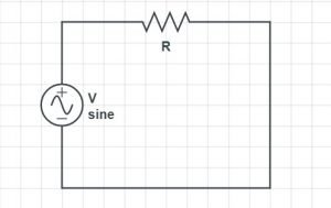
If an AC circuit only consists of a pure resistance, then that circuit will be called as Pure Resistive AC Circuit. There is no inductor or capacitor involved in this type of AC circuit. In this circuit, the power generated by the resistance and the energy components, voltage and currents, stay in an identical phase. That ensures the rise of voltage and current for the peak value or the maximum value occurs at the same time.

Pure Resistive AC Circuit

Let us assume the source voltage is V, the resistance value is R, the current flowing through the circuit is I. Resistance is connected in series. The below equation gives the voltage of the circuit.

V = Vm Sinωt

Now, from Ohm’s law, we know that V= IR, or I = V / R

So, the current I will be,

I = (Vm / R) Sinωt

Or, I = Im Sinωt; Im = Vm / R

The current and voltage will have the maximum value for ωt = 90o.

Phasor Diagram of a purely resistive circuit

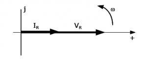
Observing the equations, we can conclude that there is no phase difference between the circuit’s current and voltage. That means the phase angle difference between the two energy components will be zero. So, there is no lag or lead in between voltage and current of the pure resistive AC circuit.

R phasor
Phasor Diagram of Pure Resistive circuit

Power in a purely resistive circuit

As mentioned earlier, current and voltage remain in the same phase in the circuit. The power is given as a multiplication of voltage and current. Proposed for AC circuits, the instantaneous values of voltage and current is taken into considerations intended for the calculation of power.

So, power can be written as – P = Vm Sinωt * Im Sinωt.

Or, P = (Vm * Im /2) * 2 Sinω2t

Or, P = (Vm /√2) * (Im/ √2) * (1 – Cos2ωt)

Or, P = (Vm /√2) * (Im/ √2) – (Vm /√2) * (Im/ √2) * Cos2ωt

Now for average power in ac circuit,

P = Average of [(Vm /√2) * (Im/ √2)] – Average of [ (Vm /√2) * (Im/ √2) * Cos2ωt]

Now, Cos2ωt comes as zero.

So, the power comes as – P = Vr.m.s *Ir.m.s.

Here, P stands for average power, Vr.m.s stands for root mean square voltage, and Ir.m.s stands for root mean square value of current.

Pure Capacitive AC Circuit

 If an AC circuit only consists of a pure capacitor, then that circuit will be called as pure capacitive AC circuit. There is not any resistor or inductor involved in this form of AC circuit. A typical capacitor is a passive electrical device that stores electrical energy in an electric field. It is a two-terminal device. Capacitance is known as the effect of the capacitor. Capacitance has a unit – Farad(F).

1 1
Pure Capacitive Circuit

When voltage is applied across the capacitor, the capacitor gets charged, and after some time, it starts discharging when the voltage source is taken away.

Let us assume that the source voltage is V; the capacitor has a capacitance of C, the current flowing through the circuit is I.

The below equation gives the voltage of the circuit.

V = Vm Sinωt

The capacitor’s charge is given by Q =CV, and I = dQ / dt gives the current inside the circuit.

So, I = C dV/dt; as I = dQ/dt.

Or, I = C d (Vm Sinωt)/dt

Or, I = Vm C d (Sinωt) / dt

Or, I = ω Vm C Cosωt.

Or, I = [Vm /(1/ωC)] sin (ωt + π/2)

Or, I = (Vm / Xc) * sin (ωt + π/2)

Xc is known as the reactance of the AC circuit (specifically the capacitive reactance). The maximum current will be observed when (ωt + π/2) = 90o.

So, the Im = Vm / Xc

Phasor Diagram of Pure capacitive circuit

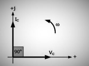
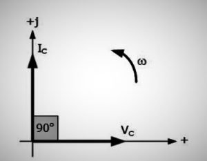
Observing the equations, we can conclude that the circuit’s voltage leads over the current value by an angle of 90 degrees. The phasor diagram of the circuit is given below.

2
Phasor Diagram of Capacitive Circuit

Power in a purely capacitive circuit

As mentioned earlier, the voltage phase has a lead over current by 90 degrees in the circuit. The power is given as a multiplication of voltage and current. For AC circuits calculations, the instantaneous values of voltage and current are taken into consideration intended for the calculation of power.

So, power for this circuit can be written as – P = Vm Sinωt * Im Sin (ωt + π/2)

Or, P = (Vm * Im * Sinωt * Cosωt)

Or, P = (Vm /√2) * (Im/ √2) * Sin2ωt

Or, P = 0

So from the derivations, we can say that the average power of the capacitive circuit is zero.

Pure Inductive AC Circuit

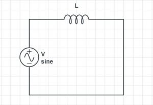
 If an AC circuit only consists of a pure inductor, then that circuit will be called as pure inductive AC circuit. There is not at all resistors or capacitors are involved in this type of AC circuit. A typical inductor is a passive electrical device that stores electrical energy in the magnetic fields. It is a two-terminal device. Inductance is known as the effect of the inductor. Inductance has a unit – Henry(H). The stored energy might also be returned to the circuit as current.

AC 3
Pure Inductive Circuit

Let us assume that the source voltage is V; the inductor has an inductance of L, the current flowing through the circuit is I.

The below equation gives the voltage of the circuit.

V = Vm Sinωt

The induced voltage is given by – E = – L dI/dt

So, V = – E

Or, V = – (- L dI/dt)

Or, Vm Sinωt = L dI/dt

Or, dI = (Vm/L) Sinωt dt

Now, applying integration on both sides, we can write.

Or, ∫ dI = ∫ (Vm/L) Sinωt dt

Or, I = (Vm/ ωL) * (- Cosωt)

Or, I = (Vm/ ωL) sin (ωt – π/2)

Or, I = (Vm/ XL) sin (ωt – π/2)

Here, XL = ωL and is known as inductive reactance of the circuit.

The maximum current will be observed when (ωt – π/2) = 90o.

So, the Im = Vm / XL

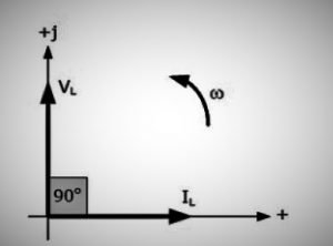
Phasor Diagram of Pure inductive circuit

Observing the equations, we can conclude that the circuit current leads over the voltage value by an angle of 90 degrees. The phasor diagram of the circuit is given below.

3
Phasor diagram for inductive circuit

Power in a purely inductive circuit

As mentioned earlier, a current phase has a lead over voltage by 90 degrees in the circuit. The power is given as a multiplication of voltage and current. For Ac circuits, the instantaneous values of voltage and current is taken into considerations utilized for the calculation of power.

So, power for this circuit can be written as – P = Vm Sinωt * Im Sin (ωt – π/2)

Or, P = (Vm * Im * Sinωt * Cosωt)

Or, P = (Vm /√2) * (Im/ √2) * Sin2ωt

Or, P = 0

So, from the derivations, we can say that the inductive circuit’s average power is zero.

MOS Capacitor: 5 Interesting Facts To Know

edrf 1024x58 1

Topic of Discussion: MOS Capacitor

  • Introduction of MOS Capacitor
  • Interface charge of MOS Capacitor
  • Working Principle in different states
  • MOS capacitance
  • MOS Threshold voltage

What is MOS Capacitor ?

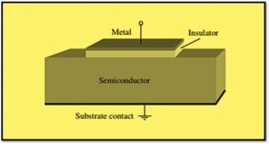
To build a A MOS capacitor, the mostly needed and major thing is the gate-channel-substrate structure.

This particular type of capacitor has two-terminals which is mainly a semiconductor device; it is made of a metal contact & a dielectric insulator.

An extra ohmic contact is given at the semiconductor substrate.

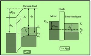
MOS Structure

The MOS structure is mostly consisted of three things:

  1. The doped silicon as the substrate
  2. Oxide Layer
  3. Insulator material: Silicon dioxide.

 Here, the insulating quality of the oxide which is uesd is quite good. The oxide-semiconductor’s density and width are very low at the particular channel accordingly.

MOS Capacitor layers

 When a bias voltage is applied,  all the charges and interferences are prevented due to the infinite resistance of the respective insulator; hence in the metal some counter charges are produced in the same layer.

The counter charges and voltage which were produced previously are used in the capacitor to control the interface charge (majority carriers, minority carriers etc). However,  the ability of fabricating a conducting sheet of minority carrier at the boundary is essential for MOS design.

Interface Charge of a MOS capacitor:

This is typically associated to the shape of the electron energy band of the semiconductor adjoining the edge. At a very low voltage,the energy band is defined by means of different properties and constructions i.e., metalic and the semiconductors. In the equation below, all the changes happened due to applied bias and voltage i.e., it becomes flat band is shown as

edrf

Where,

Øm and Øs  = work functions of the metal and the semiconductor,

rXs = semiconductor’s electron affinity,

Ec =  the energy of the conduction band edge, and

EF = Fermi level at zero voltage.

MOS Capacitor at Zero Bias and Applied Voltage:

MOS Capacitor
MOS Capacitor at Zero Bias and Applied Voltage

In this stable state, no current flow is observed in the perpendicular direction towards the high resistance of the insulator layers.

 Hence, we consider the Fermi level as constant inside the semiconductor, No other biasing will change its value.

The shifted or constant Fermi Level is shown by,

EFm – EFs = qV.

This is called quasi-equilibrium situation where the semiconductor can be used as thermal equilibrium.

When a voltage is applied in a MOS structure with a p-type semiconductor, it seems to grow upward and makes the flat band voltage negative.

In depletion mode or region, it becomes V >VFB                                               

With the increasing applied voltage and a bigger and greater energy band the difference in between the Fermi level and at the end of the conduction band at the semiconductor interface starts decreasing as well with respect to the Fermi level. Hence it becomes V = 0 V.

In higher applied voltage, the  electron concentration volume at the interface will cross the doping density of material.

ψ denotes potential differences of the semiconductors, when a place X is chosen in the semicon.

By taking consideration of electron equilibrium information, the intrinsic Fermi level Ei contracts to an different energy level qϕb from the actual Fermi level EF of selected doped semiconductor material,

 Φ = Vth ln (Na/ni)

Band
Channel formation in n-MOS MOSFET shown as band diagram: Top panels: An applied gate voltage bends bands, depleting holes from surface (left).
Image Credit : Brews ohareSemiconductor band-bendingCC BY-SA 3.0
Body Effect
Band diagram showing body effect.
Image credit : Brews ohareInversion with source-body biasCC BY-SA 3.0

MOS Capacitance:

A MOS capacitor is designed with the metallic contacts with the neutralised sections inside a doped semiconductor material. The semiconductors is also allied in series with an insulator usually prepared by silicon oxide.

The series connection between these two is presented by ,

 Ci = Sεi/di,

Wherever,

  • S = Area of MOS capacitor,
  • Cs  = capacitance of the active semiconductor,
eq 1
  • CMOS = The semiconductor capacitance can be calculated as,
eq 2

Wherever,       

  • Qs =  total charge density / area
  • ψs is the surface potential.
Illustration of C V measurement
Capacitance Voltage Characteristics of MOSFET.
Image Credit : Saumitra R Mehrotra & Gerhard Klimeck, Illustration of C-V measurementCC BY 3.0

Threshold Voltage of MOS Capacitor:

The threshold voltage is measured as V = VT . This thereshold voltage is one of the significant parameters which denotes in metal insulator semiconductor devices. The prevailing inversion may takes place if the surface potential ψs turn out to be equivalent by term 2ϕb.

The charge at the insulator-semiconductor interface of depletion layer is expressed as,

3 2

The threshold voltage applied to the ground potential is shifted by VB. A change in a MOSFET occurs when the conduction layer of moveable electron is kept at approximately fixed potentials. By taking into consideration that the inversion layer is at ground, The voltage VB is biasing the active junction amongst the inversion layer and speified substrate, and capacity of charge changeablity at depletion layer. In this case, the threshold voltage turn out to be,

4 2

The threshold voltage is changed if the surface conditions at the semiconductor oxide interface and differs within the insulated layer. The sub-threshold is hereby overlapped with the threshold voltage and the moveable carriers is increasing exponentially with the increment in applied voltage.

For more about MOSFET basics and others electronics related article  click here