Exception Handling in UFT & Synchronization (HandOn Guide!)

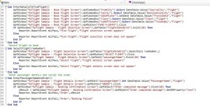
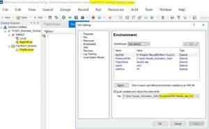
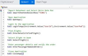
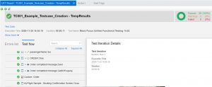
Recovery Scenario in UFT Step2 1024x474 1

In this Exception Handling in UFT and Synchronization article, we are going to learn the below topics –

· Exception Handling in UFT

· Recovery Scenario in UFT

· Synchronization in UFT

UFT Tutorial – Table of Content

Exception Handling And Synchronization in UFT

Exceptions in UFT:

An exception is nothing but an undefined event or error. In automation testing, if any errors or events are encountered which are not handled through the automated steps, they are treated as exceptions. Exceptions can be occurred due to any of the below scenarios – 

Bug – 

Any new bugs or issues in the application which are not handled properly can be the reason for an exception.

Environment Error – 

Environment outage or network latency can create exceptions as the expected screens/pages are not available.

Test data – 

Due to the correctness or invalid test data, an exception can occur during the test execution.

Technical issue – 

If the test case is not designed properly, an exception can occur during the test run.

Undefined popup – 

Any undefined popups such as Security, timeout, Information, Warning also can be the sources of exception.

The impacts of exceptions are – 

  • Test execution failure.
  • Need more effort to perform debugging/ re-execution.
  • Increase the cost and maintenance efforts.
  • Automation goal, i.e., ROI, can not be achieved.

Exception Handling in UFT: 

It is not possible to handle all the unexpected errors through automation. But if we use exception handling during the scripting, the chances of unexpected error can be minimized. The tool provides some mechanism for exception handling in UFT. The approaches for exception handling in UFT are – 

  • Recovery Scenario in UFT
  • Scripting and Test Setting
  • On-Error-Resume-Next statements for VBS
  • Using Test Settings
  • Using Exit Statement

Recovery Scenario in UFT:

A recovery scenario in UFT is an approach to handle unexpected events/ errors during the execution. The “Recovery Scenario Manager” wizard helps to manage the recovery scenarios. We can open the “Recovery Scenario Manager” by using the navigation “Resources → Recovery Scenario Manager.” While creating the recovery scenario, we need to perform three configuration steps in UFT based on the requirements. Those are Triggering Event, Recovery operations, and Post-Recovery Test Run Options.

Triggering Event: 

It defines the unexpected events, which will call the Recovery Scenario. The different options/ events available during the creation of recovery scenario in UFT are specified below – 

  • Unexpected pop-up windows.
  • Errors which may appear due to Object State.
  • Errors during the Run time.
  • Application Crash.

The main usage of recovery scenario to handle different types of unexpected errors and perform some predefined steps against each types of error.

Recovery operations: 

Based on this configuration, UFT will perform a set of actions for recovery purposes.

Post-Recovery Test Run Options: 

After the recovery, we need to configure these options to execute some predefined steps which may be required.

Step by Step guide to create a Recovery Scenario in UFT:

Now, we will learn how to create the recovery scenario in UFT based on an example.

Example – An error popup (missing mandatory fields) is appearing while trying to save the records intermittently. In this particular situation, we need to click on the OK button to close the error popup and re-execute the current step as a post-recovery action.

  • Step1#  We need to open the “Recovery Scenario Manager” from the navigation menu “Resources → Recovery Scenario Manager.”
  • Step2# Click on the “New Scenario” icon to open the wizard to create a recovery scenario in UFT and click on the Next button to select the triggering event.
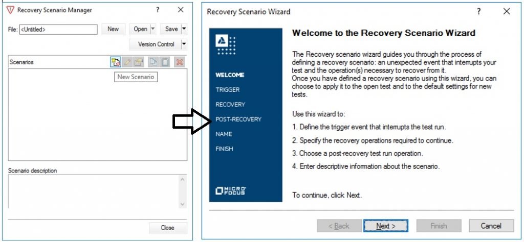
Recovery Scenario in UFT - Step2
Recovery Scenario in UFT – Step2
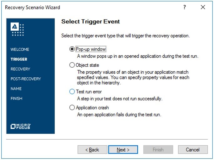
  • Step3# We need to select the “popup window” radio option as the Trigger Event of the recovery scenario and click on the Next button.
Recovery Scenario in UFT - Step3
Recovery Scenario in UFT – Step3
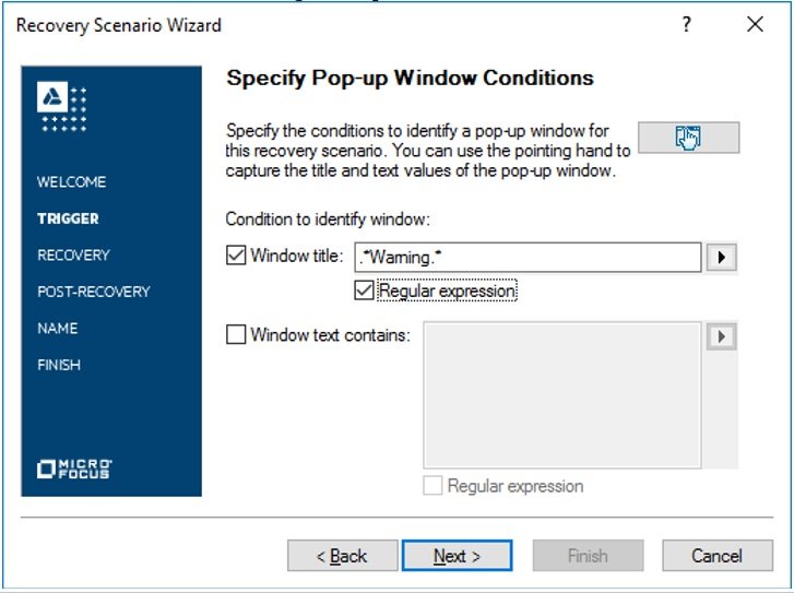
  • Step4# Now, we need to click on the pointing hand icon and identify the error popup window using the mouse. UFT tries to identify the popup based on the window title and text. So, after the identification, we can use a regular expression to make it robust.
Recovery Scenario in UFT - Step4
Recovery Scenario in UFT – Step4
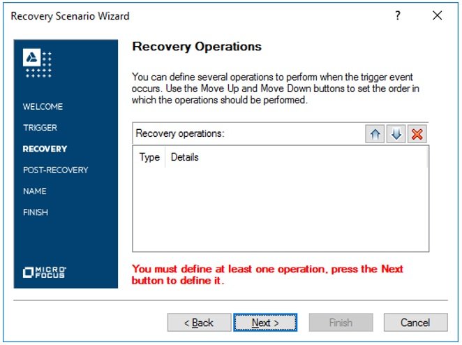
  • Step5# Initially, recovery operations are not set. To define the recovery operation, we need to click Next.
Recovery Scenario in UFT - Step5
Recovery Scenario in UFT – Step5
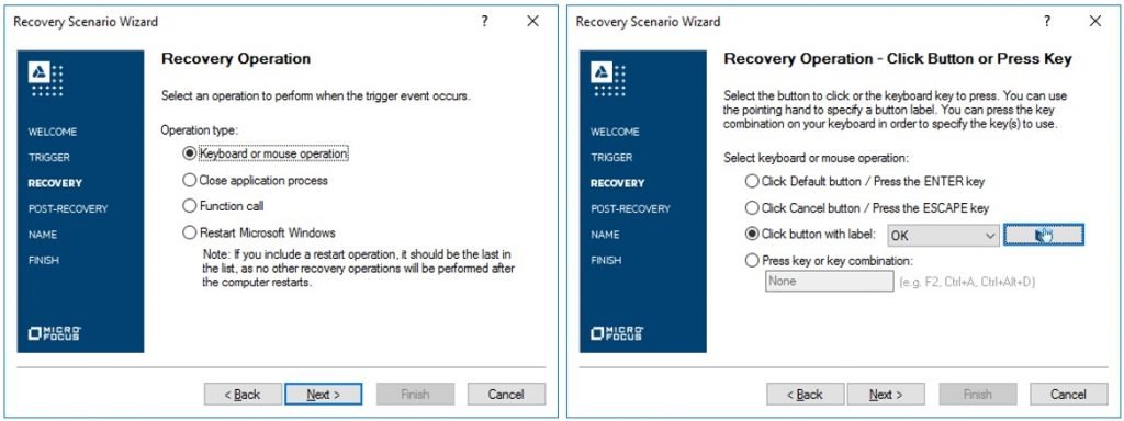
  • Step6# Now, based on our requirement, selecting “Keyboard or mouse operation.” On the next screen, select the “Click button with label” option using the pointer hand option and click on the Next button.
Recovery Scenario in UFT - Step6
Recovery Scenario in UFT – Step6
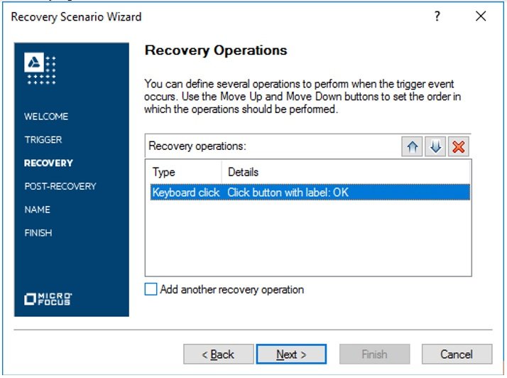
  • Step7# Recovery operation is defined now. Here, after unchecking the option “Add another recovery operation”, we need to click on “Next” button to proceed.
Recovery Scenario in UFT - Step7
Recovery Scenario in UFT – Step7
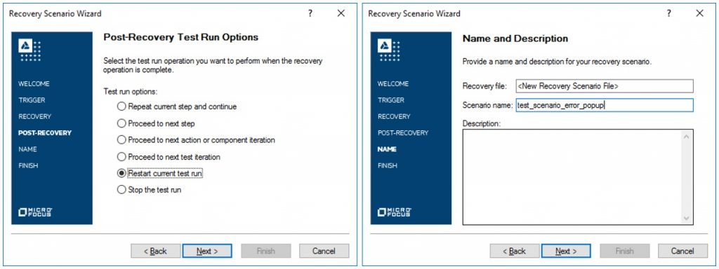
  • Step8#  We will select the option “Restart current test run” in the Post-Recovery section and provide the scenario name on the next screen. After entering the name, we need to click on “Next” button to proceed to the final screen.
Recovery Scenario in UFT - Step8
Recovery Scenario in UFT – Step8
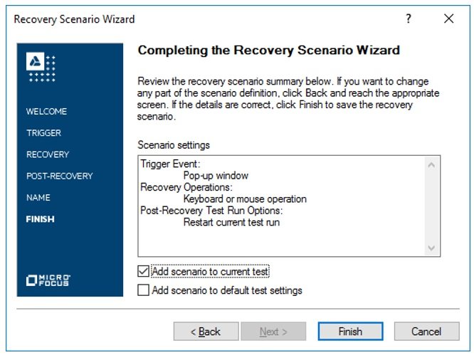
  • Step9# Based on the requirement, we can add this scenario to the current test or to the default test settings. Now, to close the “Recovery Scenario” wizard in UFT, we need to click on the “Finish” button.
Recovery Scenario in UFT - Step9
Recovery Scenario in UFT – Step9
  • Step10# Now, we need to save the recovery scenario in an external file and close.

Scripting and Test Setting Approach:

On-Error-Resume-Next statements: 

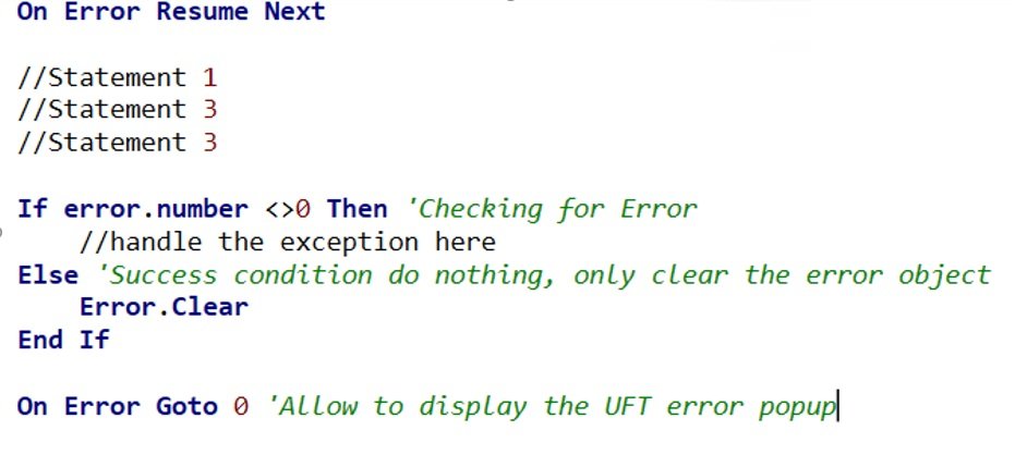
It was using the On-Error- Resume-Next statements; the exception can be handled partially. In this approach, the test script block should be started with “On Error Resume Next” statements. It defines that in case of any error, execution will will skip the present step and continue with next step. After that, by checking the error, we can handle the exceptions. Important keywords are –

On Error Resume Next – 

In case of error, UFT will not raise an error message; instead of that, execution will move to the next step.

On Error Goto 0 – 

It will work in reverse procedure with comparison to the above keyword i.e., in case of any unhandled error, an UFT error popup will be thrown with three options – retry, skip and stop.

Error.Description – 

It stores the error description.

Error.Number – 

It holds the error number. For success, the value is zero.

Error.Clear – 

It reset the Error object.
Exception Handling in UFT - On Error Resume Next Statement
Exception Handling in UFT – On Error Resume Next Statement

Using Exit Statements: 

UFT provides some predefined methods which will allow us to handle the exceptions through the scripts. The frequently used methods are –   

ExitActionIteration – 

Use to exit the current iteration of the action. ExitAction – Exits the current action.  

ExitTest – 

UFT will exit from the test execution.

ExitTestIteration –  

Skip the current test iteration and the execution will be continued with the next test iteration.

Using Test Settings:

We can configure the recovery steps by selecting any of the below options from the UFT Test Setting wizards (Run Tab).

Pop up message box 

In case of any error, UFT shows a popup message with error details.

Proceed to next action iteration –

UFT will execute the next action iteration when an exception has occurred.

Stop run –

Execution will be stopped.

Proceed to next step – 

Execution will be resumed from the next step.

Proceed to next test iteration – 

UFT will execute the next test iteration for any error.
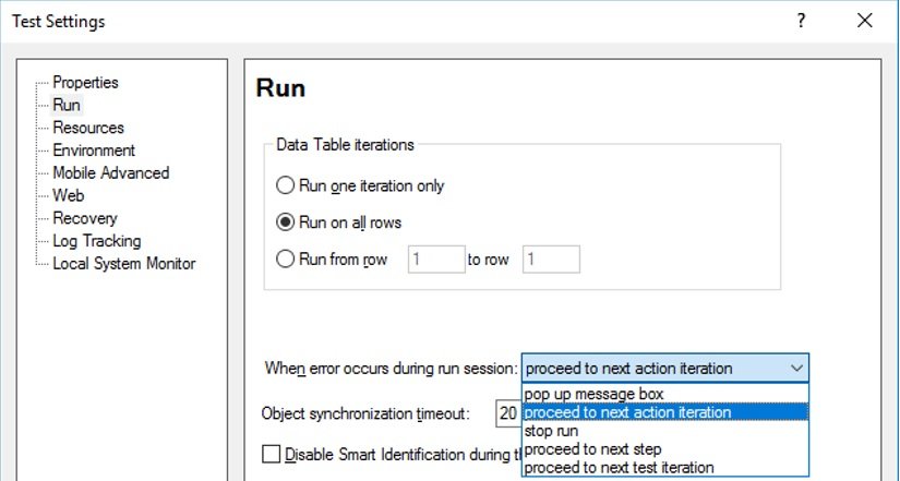
Exception Handling in UFT - Test Setting
Exception Handling in UFT – Test Setting

Synchronization in UFT:

Synchronization in UFT is an approach to define the time interface between the tool and the application under test. If the application behavior is slower than the expectation of UFT, the test will be failed. So, synchronization in UFT is another important topic for test automation.

Chances of synchronization errors can be minimized by using either of the below approaches –

Wait:  

The default Wait(timeout) statement is a static method to handle the synchronization errors. Here, timeout denotes the hardcoded wait time in seconds. During the execution, the script will wait for specific time at this point. We need to define the value of timeout based on the application responses.

WaitProperty in UFT:

To use the method WaitProperty in UFT, we need to specify the property name, the expected value of the property and the maximum wait time in mili-seconds. This is a dynamic way to handle the synchronization. Here, the execution will wait till the the property value satisfies with the expected value in the application. If the property value does not match, after the spefied maximum timeout, the script will proceed with the next step. Example –

Window(“<windiow name>”).WinListView(“<view name>”).WaitProperty “visible”,true,20000

  • Loop:

This is an indirect way to handle the synchronization dynamically. We can use a loop with a condition to check the the object’s property value does not satisfied with expected value. In the loop statement, we can provide a small time out value using the Wait(timeout) statement. So, the checking will be done after each timeout and loop will be continued until the object is visible.

  • Test Setting:

 We can define the synchronization timeout in the Test Setting wizard (Run tab and web tab for web navigation timeout). Based on this configuration, UFT will wait for the test objects.

Conclusion:

In this “Exception Handling in UFT ..” article, we have learned about exception handling in UFT along with recovery scenarios and synchronization in UFT. Please click here to get more information on “Exception Handling” from the Microfocus support portal.

7 Facts On Multiplexer And Demultiplexer: Beginner’s Guide !

  • Definition & Overview of Multiplexer
  • Operation & Analysis
  • Implementation of Boolean Function using MUX
  • DEMUX
  • Application of MUX-DEMUX

Definition:

A digital multiplexer is a device that takes more than one inputs and outputs a single selected data. Just like an adder and subtractor, a multiplexer is also a combinational device.

It is also identified as a data selector as it pick out one of several inputs and sends it to the output with the help of a control signal or select lines. If a typical MUX has 2n input lines, then there will be n choose lines. The bit combination of select lines determines which output will be produced.

2:1 MUX Definition:

A 2:1 MUX signify that the multiplexer has two input and one output. It also has one select line as S. If S =0, the upper AND gate are ON, and I0 appears at the o/p, and if the S =1, the lower AND gate is ON and I1 appears at the o/p. MUX acts like a switch which chooses one out of two available input.

Multiplexer 2 to 1
A 2:1 Multiplexer with the Boolean equation, Image source – en:User:CburnettMultiplexer 2-to-1CC BY-SA 3.0

4:1 MUX Definition:

A 4:1 MUX means that the multiplexer has four input lines and one output line. It has two select lines as S0 and S1. There are several AND gates to produce the output. Select lines are connected with the correspondent AND gates. The result of AND gates are connected to a single OR gate.

If the select lines give the binary code as 10, that is, S1 = 1 and S0 = 0, then the AND gate connected with input I2 has two of its inputs equal to value 1, and the last one is connected with I2. The other three AND gates have at least one input equal to zero, this correspondingly changes their output equal to zero. Here and now, the outcome of the OR gate is analogous to the value of I2 and allows the designated input to look as if at the result. 

Multiplexer 4 to 1
A 4:1 Multiplexer block diagram, Image by – en:User:CburnettMultiplexer 4-to-1CC BY-SA 3.0

Operation & Analysis

A multiplexer is very much similar to a decoder. The AND gates and the NOT gates bring the similarity between a decoder and multiplexer. Meanwhile, a MUX truly decodes the select lines and provides the output. A multiplexer can also be constructed from a decoder. If 2n input lines – each to AND gate are added up with an n to 2n decoder, the circuit will work as a multiplexer.

The multiplexer size depends on the data input lines that are 2n and the single output line. The number of selection lines will be n for a 2n input line mux. Like a decoder, a mux may also have an enable input line. The outputs will be disabled if the enable input is in an inactive state. When the enable pin is in an active state, the MUX will work as usual.

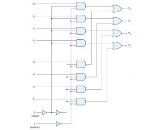
There are efficient techniques to be responsible for multiple bit selection-logic. If the multiplexer circuits are combined with standard selection inputs, the numerous bit selection can be implemented. To implement this, a quadruple 2:1 mux is shown in the below image.

MUX
Quadruple MUX

Here, the circuit has four multiplexers, and they are 2:1 mux. The output Y0 can be selected from input A0 or B0. Similarly, the output of Y1 can be selected from input A1 or B1, and it continues for the rest of the circuit. The select lines S selects one of the lines for each of the multiplexers. The enable input must be in an active state to operate the multiplexers.

Though the circuit has a 2:1 multiplexer for operation, it looked like a circuit that pick out anyone of the two 4 -bit sets of data line. Now, when the enable is 0, and the select line is also 0, the four an inputs can appear as the output. Also, if the s=1, then the B inputs appear at the result. The outcomes will be 0 when the enable pin is set to 0, no matter the value of select lines.

Implementation of Boolean Function using MUX

Boolean functions can also be implemented using multiplexers. The min-terms of a function can be generated in a multiplexer with the circuit connected with the selection lines. The data inputs can select separate min-terms. This is how implementations of n variable function are possible for a multiplexer of input data lines of 2n and n select lines. The input data lines will be used for each min-term.

A more efficient way to implement Boolean expression is also available. A function of n variables can be implemented with a multiplexer having n-1 lines. The first n-1 variable is utilized as selection inputs. The remaining variable of the operation is used for data inputs. If each data input denotes the remaining variable, the mux will be a, a’, 1, or 0.

We can take the example of a Boolean algebra.

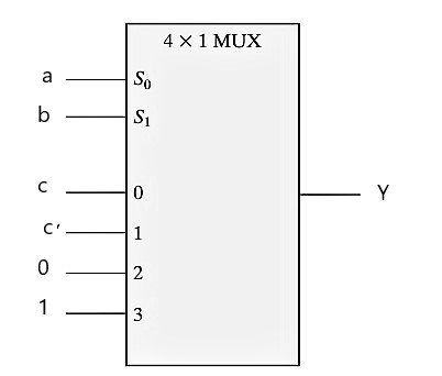
F (a, b, c) = ∑ (1, 2, 3, 4)

The function of three variables can be implemented with a 4:1 MUX, as shown below.

BOOLEAN MUX
Implementation of Boolean Functions

The two variables, a and b, are applied to the select lines in a certain order. The a  is connected to the S1 input, and b is linked with the S0 input. The truth table of the function determines the values for the input lines of the MUX. When ab = 00, output F is equal to c as F = 0 when c = 0 and F = 1 when c = 1. Data input 0 requires the input for variable c.

The multiplexer works in a certain way. When the value of ab is zero, then the data input 0 appears at the output. Thus, the output becomes equal to c. The data lines 1, 2, 3 also required inputs and can be determined similarly. The inputs are derived from the function F, and the inputs are ab = 01, 10, 11.We can find out the inputs for the data lines by this explanation.

This example shows the typical steps to implement Boolean functions consisting of n variables with the help of a multiplexer with n – 1 selectionline and 2n-1 dataline. The truth table of the Boolean function is described initially. The primary n-1 variables of the process given are applied to the selection input of the MUX. The output is calculated as the last variable’s function for every single combination of the selection lines. The process has a specific set of values. The function’s value can be 0 or 1, or the variables or the complement of the variables.

Now let us take an example of a more considerable Boolean function.

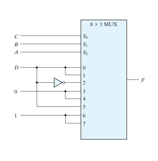
F (A, B, C, D) = ∑ (1, 3, 5, 7, 9, 11, 13, 15)

A multiplexer can implement this Boolean function with three select lines and eight input lines (Basically an 8:1 MUX). The MUX is shown in the image.

BOOLean MUx 2
8 x 1 MUX

Now, the first variable that is A, should be connected to the select line S2 to make sure the correspondent select lines for B and C becomes S1 and S0. The truth table of the function is depicted as mentioned earlier. The values for the input lines for the MUX is calculated from that truth table. The data line number is determined by the binary combinations of the variable ABC.

If ABC = 101, then F comes as D. Form this, it can be calculated that data input line 5 receives input as D. Logic 0 and logic 1 are two fixed values. Logic 0 means logic low or equivalent to ground, and logic 1 means logic high or the input power signal.

Three State Gates

The construction of a multiplexor is possible using three-state gates. Three state gates are the digital circuitries that can operate in three states. Two out of those three states are 0 and 1 conventionally, and the third state is known as the high impedance state. At the high impedance state, the logical procedure performs like an open circuitry. Three state gates can perform all types of logical operations, such as NOT or NOR. The most common use of a three-state gate is as a buffer gate.

As said earlier, multiplexers can be constructed using three-state buffers. The image below describes the implementation of a 2:1 mux with two three-state buffer and a NOT gate. The two outputs are connected for providing a single result. When the select line is valued as zero, the upper pad gets activated, and the lower one gets disabled. A appears at the output, and when the select input is 1, the reverse happens, and B appears at the result.

DEMUX

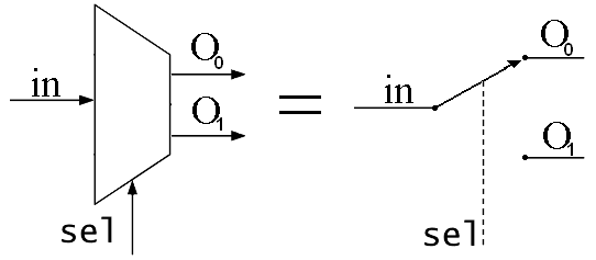
A DEMUX or de-multiplexer is a digital device that does the opposite of a multiplexer. It takes a single input and provides multiple outputs with the help of select lines. If a DEMUX has n select lines, then the numbers of production will be 2n. A diagram of 4:1 DEMUX is given below.

A Demultiplexer , Image Credit – FresheneeszDemultiplexerCC BY-SA 3.0

MUX & DEMUX Applications:

MUX and DEMUX have importance in today’s digital era. Some of their applications are –

Mux-Demux,Image – Tony R. Kuphaldt, Telephony multiplexer systemCC BY 1.0
  • Communication System: MUX and DEMUX have the most extensive applications in the field of communication systems. MUX allows transmitting distinct types of data like – audios and video, images, voice recordings, etc. can be multiplexed into a single transmission channel. It increases the efficiency of the system.
  • Telephonic System: Telephone networks need both MUX and DEMUX. Technologies like – Frequency Division Multiplexing (FDM), Time Division Multiplexing (TDM), Code Division Multiple Access (CDMA), etc., are possible only because of MUX and DEMUXs.
  • MUX and DEMUXs are also used in logic gates for combinational circuits and many other digital devices.

7 Facts On Binary Subtractor: Half & Full Subtractor

Half subtractor using NAND 300x155 1
  • Definition and Overview of Binary Subtractor
  • Half Subtractor
  • Full Subtractor
  • N -bit Subtractor
  • Applications of binary subtractor
  • VHDL implementation of half subtractor and full subtractor

Definition

A subtractor is a device that subtracts two numbers and produces the result. A digital or binary subtractor is something that deals with the Subtraction of binary digits.

A binary subtractor is needed for digital computation inside a digital device or a digital computer. The most convenient way of Subtraction unsigned binary numbers is the method of complements. There are rules for binary Subtraction.

The binary subtraction rules are stated as follows. Here 0 is logic low, and one is logic high. A and B are two inputs.

ABY = A – B
000
011 (borrow 1)
101
110
Binary Subtraction truth table

Example of subtraction operations:

1101 – 1011

1101

– 1011

= 0010

So, the answer is 0010

Methods of complements can alternatively carry out binary subtractions for binary subtractors. There are two types of complement methods that are generally used.

A.  1’s Complement

B. 2’s Complement

Steps for performing 1’s complement:

  1. Find out the 1’s complement of the number that is to be subtracted.
  2. Now the 1’s complement is added to the number from which the Subtraction is desired.
  3. Where there is one carry in the last position, of the result of the addition in step 2, the carrier is removed and added to the product without the carry to obtain the final result.

Let us take an example – 1101 – 1011

1’s complement of 1011 = 0100

Now, add 1101 with 0100

1101

 + 0100

 = 1 0001

As we can see, there is one as a carry, so we remove the carry and add the carry again with the obtained result.

0001

+    1

= 0010

So, the answer to the Subtraction is 0010

For 2’s complement method

  1. Calculate the 2’s complement.
  2. The complement is now added with another number.
  3. The carry is rejected.

Let us take an example – 1101 – 1011

2’s complement of any number is calculated by performing 1’s complement and adding 1 to it.

2’s complement of

Now, add 1101 with 0100

1101 + 0100 = 1 0001

As we can see, there is one as a carry, so we remove the carry and add the carry again with the obtained result.

0001 + 1 = 0010

So, the answer to the Subtraction is 0010

Digital computers use the 2’s complement method for calculations as it requires less carry.

The complement methods in the decimal number system are known as 9’s and 10’s complement method.

Various digital circuitries implement this subtraction operation. They are –

  • Half Subtractor
  • Full Subtractor

A binary subtractor not only performs addition operations but also used in digital applications. Decoding and encoding of values, calculation of the index is a few of its applications.

Half subtractor

A half binary subtractor is a binary subtractor that subtracts one bit of data and produces the result. It has two input sides through which we supply the digital logic values, and it has two outputs through which we receive the impact of the operation. The result can be shown in a single digit. The work shows the number in the Subtraction that has the same significance as the individual digits subtracted. The other output shows the borrow bit.

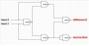
Half subtractor using NAND
NAND gate implementation. Image Credit – NitianabhigyanHalf subtractor using NANDCC BY-SA 4.0

The half subtractor truth table

The working of the half binary subtractor is shown in the following truth table.

ABDifferenceBorrow
0000
0111
1010
1100
Truth table for half binary subtractor

Half Subtractor circuit

From the truth table, we can conclude that the first three rows can represent the result using a single digit. In the second row, the work is described using two numbers as it has borrowed as 1.

Difference = A′B + AB′

Borrow = A′B 

So,

Difference = A XOR B

Borrow = A′ AND B

We need one XOR gate, one NOT gate, and one AND gate to implement the logic. XOR gate, NOT gate, an AND gate can also be made using universal gates like NAND and NOR. So, a half subtractor can be designed using only universal gates.

The following image shows A and B as the input and D as the difference, and C as they borrow.

Half  Binary Subtractor
Half Subtractor

Full Subtractor

Full Binary Subtractor is another kind of binary Subtractor which provides the result of a binary subtraction operation. When two binary numbers are subtracted, except for the least significant digit, there is a borrow-in as Bi-1 and borrow out as Bi. The full Subtractor is designed to handle a borrow-in for each stage. That is how an entire order overcomes the shortcoming of half Subtractor of running borrow-in.

A full subtractor truth table

XiYiBi-1DiBi
00000
00111
01011
01101
10010
10100
11000
11111
Full Subtractor truth table

Full subtractor circuit

Difference = A′ B′ Bin + A B′ Bin′ + A′ B Bin′ + A B Bin 

Borrow = A′ Bin + A′ B + B Bin 

To implement the expression using logical gates, we need to simplify the word further.

Difference = A′ B′ Bin + A B′ Bin′ + A′ B Bin′ + A B Bin 

 Or, Difference = Bin (A′B′ + AB) + Bin ′ (AB′ + A′B)

 Or, Difference = Bin (A XNOR B) + Bin ′ (A XOR B)

 Or, Difference = Bin (A XOR B) ′ + Bin ′ (A XOR B)

 Or, Difference = Bin XOR (A XOR B)

  Or, Difference = (A XOR B) XOR Bin

Borrow = A′ B′ Bin + A B′ Bin′ + A′ B Bin′ + A B Bin 

 Or, Borrow = A′ B′ Bin +A′ B Bin ′ + A′ B Bin + A′ B Bin + A′ B Bin + A B Bin

 Or, Borrow = A′ Bin (B + B′) + A′B (Bin + Bin ′) + B Bin (A + A′)

 Or, Borrow = A′ Bin + A′B + B Bin

The expression can be written in another way –

Bout = A′ B′ Bin + A′ B Bin′ + A′ B Bin + A B Bin     

    Or, Borrow = Bin (AB + A′ B′) + A′ B (Bin + Bin′)

     Or, Borrow = Bin (A XNOR B) + A′ B

    Or, Borrow = Bin (A XOR B) ′ + A′ B

Full Binary Subtractors
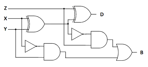
Full Subtractors , X,Y, Z are input

As the circuit diagram shows, A, B, and Bin. The circuit gives two output as difference output and borrows output. The Bin is set to 1 whenever there is borrow in input A. Bin is then subtracted from A and Y.

The general expression can be written as D = A – B – Bin + 2 Bout.

Full subtractors can also be implemented using half subtractors.

1920px Full sub Fixed.svg
Full Subtractors using Half Subtractor

N bit Subtractor

In a single bit binary subtractor, Subtraction of only 1 bit can be performed. If we need to perform Subtraction of n -bit, then a n bit binary subtractor is required. An n-bit subtractor can be implemented similarly using subtractors in a cascaded form.

Applications of Subtractors

  • Subtractors are often used with adders. Whenever an adder is needed for a circuit, a subtractor is also required.
  • ALU, which is responsible for the calculation, and stays inside a microprocessor, also needs subtractors. CPUs also need subtractors for operation.
  • Microcontrollers also use subtractors for performing the digital computation.
  • Subtractors are also used in Digital Signal Processing Domain.
  • Digital computers use a lot of subtractors.

VHDL Implementation of Half Subtractors & Full Subtractors

Half Subtractor Data flow Modelling

library IEEE;

use IEEE.STD_LOGIC_1164.ALL;

entity ENTITY_NAME is

    Port ( A : in  STD_LOGIC;

           B : in  STD_LOGIC;

           IB : in  STD_LOGIC;

           Diff : out  STD_LOGIC;

           Borr : out  STD_LOGIC);

end ENTITY_NAME;

Architecture Dataflow

architecture Dataflow of ENTITY_NAME is

begin

Diff <= (A xor B) xor IB;

Borr <= ((not A) and (B or IB)) or (B and IB);

end dataflow;

Full Subtractor Dataflow Modelling

entity ENTITY_NAME  is

    Port ( A : in  STD_LOGIC;

           B : in  STD_LOGIC;

           IB : in  STD_LOGIC;

           Borr : out  STD_LOGIC;

           Diff : out  STD_LOGIC);

end ENTITY_NAME;

Architecture dataflow

architecture Behavioral of ENTITY_NAME is

begin

process(A,B,IB)

begin

if(A=’0′ and B=’0′ and IB=’0′ )then

Diff<=’0′;

Borr<=’0′;

elsif(A=’0′ and B=’0′ and IB=’1′ )then

Borr<=’1′;

Diff<=’1′;

elsif(A=’0′ and B=’1′ and IB=’0′ )then

Borr<=’1′;

Diff<=’1′;

elsif(A=’0′ and B=’1′ and IB=’1′ )then

Borr<=’0′;

Diff<=’1′;

elsif(A=’1′ and B=’0′ and IB=’0′ )then

Borr<=’1′;

Diff<=’0′;

elsif(A=’1′ and B=’0′ and IB=’1′ )then

Borr<=’0′;

Diff<=’0′;

elsif(A=’1′ and B=’1′ and IB=’0′ )then

Borr<=’0′;

Diff<=’0′;

else

Borr<=’1′;

Diff<=’1′;

end if;

end process;

end Behavioral;

Laser Drilling: A Comprehensive Guide for Science Students

laser drilling

Laser drilling is a highly precise and versatile manufacturing process that uses a laser beam to create holes in various materials. This process is characterized by its ability to produce high-quality holes with minimal heat-affected zones (HAZ) and excellent roundness. The quality of laser-drilled holes can be evaluated using several metrics, including roundness, Hillock ratio, taper, and HAZ.

Understanding the Fundamentals of Laser Drilling

Laser drilling is a non-contact, thermal-based material removal process that utilizes the high energy density of a focused laser beam to vaporize and eject material from the workpiece. The process involves the following key steps:

  1. Laser Beam Absorption: The laser beam is absorbed by the surface of the workpiece, causing localized heating and melting of the material.
  2. Material Removal: The intense heat generated by the laser beam causes the material to vaporize, creating a small hole or cavity in the workpiece.
  3. Ejection of Molten Material: The vaporized material is ejected from the hole, leaving behind a clean, high-quality opening.

The efficiency and quality of the laser drilling process are influenced by various parameters, including laser power, pulse duration, repetition rate, beam diameter, and the properties of the workpiece material.

Evaluating the Quality of Laser-Drilled Holes

laser drilling

The quality of laser-drilled holes can be assessed using several key metrics:

Roundness

The roundness of a laser-drilled hole is calculated as the average of the elliptical roundness at the entrance and exit sides of the hole. The elliptical roundness is calculated using the shorter or minor elliptical diameter and the longer or major elliptical diameter at the entrance or exit side of the hole. An average roundness of 1 indicates the best quality, with larger values indicating better drilling quality for an ideal circle.

The formula for calculating the elliptical roundness (ER) is:

ER = (Minor Diameter / Major Diameter) × 100%

Hillock Ratio

The Hillock ratio is a measure of the height of the hillock, or raised area, surrounding the hole relative to the diameter of the hole. A lower Hillock ratio indicates better drilling quality, with a value of 0 being the ideal.

The Hillock ratio (HR) is calculated as:

HR = Hillock Height / Hole Diameter

Taper

Taper is a measure of the change in diameter of the hole along its depth. A lower taper value indicates better drilling quality, with a value of 0 being the ideal.

The taper (T) is calculated as:

T = (Entrance Diameter – Exit Diameter) / Hole Depth

Heat-Affected Zone (HAZ)

The HAZ is the area around the hole that has been affected by the heat generated during the drilling process. A smaller HAZ indicates better drilling quality, with minimal distortion and damage to the material.

The size of the HAZ can be measured using various techniques, such as optical microscopy or scanning electron microscopy (SEM), and is typically reported in micrometers (μm).

Optimizing Laser Drilling Parameters

The quality of laser-drilled holes can be optimized by adjusting various control factors, such as laser pulse energy, repetition rate, focusing position offset, and drilling time. A study using a Quantel Brilliant Neodymium-doped Yttrium Aluminum Garnet (Nd: YAG) laser with a pulse width of 5-6 ns and F-theta lenses to deliver a focused laser beam with a diameter of 0.2 mm found the optimal combination of control factors to be A1B3C1D1, with a maximal variation of 0.406 obtained from the control factor B (focusing position offset), which had the greatest contribution to the drilling time.

Table 1: Optimal Combination of Control Factors for Laser Drilling

Control Factor Optimal Setting
A (Laser Pulse Energy) A1
B (Focusing Position Offset) B3
C (Repetition Rate) C1
D (Drilling Time) D1

By understanding the relationships between these control factors and the resulting hole quality, laser drilling can be optimized to achieve the desired performance characteristics.

Advanced Techniques in Laser Drilling

Researchers have explored various advanced techniques to enhance the capabilities of laser drilling, including:

  1. Dual-Beam Laser Drilling: This technique uses two laser beams, one for drilling and the other for assisting the drilling process. The assisting beam can help to reduce the HAZ and improve the quality of the drilled holes.

  2. Underwater Laser Drilling: Performing laser drilling in a water-assisted environment can help to reduce the HAZ and improve the quality of the drilled holes by providing efficient cooling and debris removal.

  3. Laser-Induced Plasma Assisted Drilling (LIPAD): LIPAD utilizes a laser-induced plasma to enhance the material removal rate and improve the quality of the drilled holes. The plasma can help to increase the absorption of the laser energy and facilitate the ejection of the molten material.

  4. Femtosecond Laser Drilling: Femtosecond lasers, with pulse durations in the range of 10^-15 seconds, can produce high-quality, low-HAZ holes by minimizing the thermal effects on the workpiece material.

  5. Hybrid Laser Drilling: Combining laser drilling with other techniques, such as mechanical drilling or electrical discharge machining, can help to improve the efficiency and quality of the drilling process.

These advanced techniques demonstrate the ongoing research and development in the field of laser drilling, aimed at addressing the challenges and expanding the capabilities of this versatile manufacturing process.

Applications of Laser Drilling

Laser drilling has a wide range of applications across various industries, including:

  1. Aerospace: Laser drilling is used for creating cooling holes in turbine blades, fuel injector nozzles, and other aerospace components.
  2. Electronics: Laser drilling is employed for creating vias (vertical interconnects) in printed circuit boards and microelectronic devices.
  3. Automotive: Laser drilling is used for creating fuel injection holes, cooling holes, and other precision features in automotive components.
  4. Medical: Laser drilling is utilized for creating micro-holes in medical devices, such as stents, catheters, and drug delivery systems.
  5. Jewelry and Watchmaking: Laser drilling is employed for creating intricate patterns and features in jewelry and watch components.

As the demand for high-precision, high-quality manufacturing continues to grow, the applications of laser drilling are expected to expand further, driving the need for continued research and development in this field.

Conclusion

Laser drilling is a highly precise and versatile manufacturing process that can produce high-quality holes with minimal heat-affected zones and excellent roundness. By understanding the fundamental principles, evaluating the quality metrics, and optimizing the control factors, laser drilling can be leveraged to address a wide range of industrial and technological challenges. The ongoing advancements in laser drilling techniques, such as dual-beam, underwater, and femtosecond laser drilling, further expand the capabilities of this innovative manufacturing process.

References

  1. Quantitative Analysis of Holes Produced in Laser Micromachining, https://asmedigitalcollection.asme.org/manufacturingscience/article-pdf/doi/10.1115/1.3123341/5934933/031011_1.pdf
  2. Multi-Objective Optimization of Nd: YAG Laser Drilling of Optical Components, https://www.ncbi.nlm.nih.gov/pmc/articles/PMC9785554/
  3. Review on laser drilling I. Fundamentals, modeling, and simulation, https://pubs.aip.org/lia/jla/article-abstract/25/1/012006/221181/Review-on-laser-drilling-I-Fundamentals-modeling?redirectedFrom=fulltext
  4. Laser Drilling of Metals: A Review, https://www.sciencedirect.com/science/article/abs/pii/S0924013613000749
  5. Laser Drilling: A Review, https://www.tandfonline.com/doi/abs/10.1080/10426914.2013.811637

7 Facts On Facts On Binary Adder:Full Adder & Half Adder

Half Adder 300x167 1
  1. Definitions and Overview of adder
  2. Types of adder
  3. Half adder
  4. Full adder
  5. BCD adder

Definitions:

An adder is a device which add up two numbers and produce the result. A binary adder is something which deals with addition of binary numbers.

A binary adder is a digital device and needed for digital computations. The operation performed in a binary adder, obeys the rules of binary addition. Here two bits corresponding to 2n are added and the resultant is then added to the carry from the 2n-1 digit.

The binary addition rules are stated as follow. Here 0 is logic low and 1 is logic high. A and B are two inputs.

ABY = A + B
000
011
101
110 (carry 1)
Binary Addition

Example of addition operations:

  • 11111 + 1011 + 101 + 10 + 1
  • 11111+ 1011 = 101010
  • 101010 + 101 = 101111
  • 110001 + 1 = 110010

So the answer is 110010

Types of Adder

This addition operation is implemented by various digital circuitries. They are –

  • Half Adder
  • Full Adder
  • BCD Adder

A binary adder not only performs addition operations but also used in other digital applications. Decoding of address, calculation of index are few of its applications.

Half Adder

A half adder is a type of binary adder which add one bit of data and produces the result. It has two input side through which we supply the digital logic values and it has two outputs through which we receive the result of the operation. The result can be shown in a single digit. The output shows the digit in the sum that has the same significance as the individual digits added. The other output shows the carry bit.

Half Adder Truth table

The operation of the half adder is shown in the following truth table.

ABSumCarrySum of A & B
000000
011001
101001
110110
Truth Table of Half Adder

Now from the truth table, we can observe that the first three rows can represent the sum using a single digit. At the last row, the sum is represented using two digits as it has 1 as carry. Here the sum is zero and carry 1 must be taken to the position of next higher significance.

Sum = A′ B + A B′

Carry = AB

So,

Sum = A XOR B

Carry = A AND B

To implement the logic, we need one XOR gate and one AND gate. XOR gate and AND gate can also be made using universal gates like NAND and NOR. So, a half adder can be designed using only universal gates.

The following image shows A and B as the input and S as the sum and C as the carry.

Full Binary Adder
Half binary adder , Image Source – inductiveloadHalf Adder, marked as public domain, more details on Wikimedia Commonsmedia

Full Adder

Another type of binary adder is full adder. It also adds binary data and produces the output. Now, when two binary numbers are added, except the least significant digit there is a carry-in as Ci-1 and carry-out as Ci. The full adder is designed to handle a carry-in for each stage. That is how a full order overcomes the shortcoming of half adder of handling carry-in.

Full adder truth table

AiBiCi-1SiCi
00000
00110
01010
01101
10010
10101
11001
11111
Full Adder Truth Table

Full Adder Circuit

Si = Ai Bi Ci-1 + Ai Bi Ci-1 + Ai Bi Ci-1 + Ai Bi Ci-1 + (Ai Bi + Ai Bi) Ci-1   + (Ai Bi + Ai Bi) Ci-1

And the carry comes as:

Ci = Ai Bi Ci-1 + Ai Bi Ci-1 + Ai Bi Ci-1 + Ai Bi Ci-1 

Or, Ci = (Ai Bi + Ai Bi) Ci-1   + (Ai Bi + Ai Bi) Ci-1

Or, Ci = Ai Bi + (Ai Bi + Ai Bi) Ci-1

Now, consider a half adder has inputs A and B. The output sum is S and carry is C. Now the expression of Si and Ci can be obtained from the expressions of Sum and carry of half adder circuit.

Si = S Ci-1 + S Ci-1

Ci = C + S Ci-1

Now, to implement a full adder using half adders we need two half adders and one OR gate. Full adder implementations using half adders is represented in the below figure.

Full adder logic diagram
Full binary adder , Image Source – InductiveloadFull-adder logic diagram, marked as public domain, more details on Wikimedia Commons

As we can see in the figure that the first half adder (marked as-) has the input Ai and Bi. The second half adder (marked as-) has inputs of C i-1 and output of the first half adder that is S. The output of the second half adder are Si and S Ci-1.

Now, S Ci-1 represents the carry out. The carry of the first half adder that is C and the carry of the second half adder that is S Ci-1 are fed as input of a OR gate. The output of the OR gate is the final carry out of the full adder circuit.

Parallel Binary Adders

A full adder is needed for the addition of bits in each stage of addition except the addition of least significant digits on the other hand two half adders are needed to complete a full adder. It follows the rule that the addition of two n-bit numbers will require 2 * m -1 number of half adder and m-1 numbers of OR gates. This type of binary adders is known as parallel binary adders. The speed of operation of these types of adders are very fast. That is why they are preferred in modern computational devices.  

Let us add 101 and 111 as an example of parallel binary adder. The figure shown below represents the addition.

4 bit carry lookahead adder
Parallel binary adder, Image source – en:User:Cburnett4-bit carry lookahead adderCC BY-SA 3.0

The first half adder (marked as-1) adds the extreme right-hand bits 1 and 1 to produce the binary sum 0 and the carry 1 according to the rules of binary addition. The output of the half adder is fed into the input of the first full adder (marked as- 2). The other two inputs of first full adder are the two next bits that is 0 and 1. The outputs of the first full adder are 0 as sum and 1 as carry. They are further fed into input of second full adder. The other two inputs are 1 and 1. The outputs of the second full adder is 1 as sum and 1 as carry. So, the result of the summation is 1100.

Now, a point to be noted that in place of a half adder at the least significant digit position, a full adder can be used with its carry input made 0.

BCD Adder

The term BCD in BCD adder stand for Binary Coded Decimal. BCD is a special type of binary encoding where each digit has certain number of bits for representation. The BCD of first 10 decimal value is shown in the table.

Decimal Digit BCD  
00000
10001
20010
30011
40100
50101
60110
70111
81000
91001
BCD ADDER

BCD adder has two inputs which varies from 0 to 9. The output varies from 0 to 18 and if the previous carry is considered then the range will be up to 19.

The table for BCD adder is given below.

decimal or bcd adder
BCD Adder Truth Table

From the above table, we can observe that from 1 to 9 the binary and the BCD is same. From 10 to 19 decimal numbers, both the binary and codes are different.

The circuit diagram of a BCD adder is shown below.

  • In the above diagram there is a four-bit binary adder which has input as addended and augend. It has also input of carry.
  • The binary adder gives output of the addition and an carry output.
  • Now, using the output and the carry the circuit is further designed to find out the final carry.
  • The output is further fed into a 4-bit adder.
  • Now, the circuit is designed to make the 1st and 4th bit of the addended number as 0 and also the 2nd and 3rd bit to make as same as Carry. When the carry is 1, the circuit is designed in such a way that the addended will be 0110. 6 is added with augend to get the BCD.

Example of BCD

0110 + 0101 = 1011

Now this is invalid as BCD. The number is greater than 9. So, we have to add 6 to the result.

The final result will be = 1011 + 0110 =

1011 + 0110 = 10001

So the final answer will be 10001

Know about Subtractors! Click Here!

VHDL implementation of Half adder and Full Adder

HALF-BINARY ADDER DATAFLOW MODELLING

library IEEE ;

use IEEE.std_logic_1164.all ;

entity half_adder_dataflow is

    Port ( a : in  STD_LOGIC;

           b : in  STD_LOGIC;

           s : out  STD_LOGIC;

           c : out  STD_LOGIC);

end half_adder_dataflow;

architecture Behavioral of half_adder_dataflow is

begin

s <= a XOR b;             

c <= a AND b;            

end Behavioral;

HALF- BINARY ADDER BEHAVIORAL MODELLING:

entity SUDIPTA_ROY_HALFADD is

    Port ( A : in  STD_LOGIC;

           B : in  STD_LOGIC;

           C : out  STD_LOGIC;

           S : out  STD_LOGIC;

           Z : out  STD_LOGIC);

end SUDIPTA_ROY_HALFADD;

architecture Behavioral of SUDIPTA_ROY_HALFADD is

begin

process(A, B)

begin

if(A=’0′ and B=’0′) then

S <=’0′;

C <=’0′;

elsif(A=’0′ and B=’1′) then

S <=’1′;

C<=’0′;

elsif(A=’1′ and B=’0′) then

S <=’0′;

C<=’1′;

else

S <=’1′;

C<=’1′;

end if;

end process;

end Behavioral;

FULL-ADDER DATAFLOW MODELLING

library IEEE;

use IEEE.STD_LOGIC_1164.ALL;

entity SUDIPTA_ROY_FULLADD is

    Port ( A : in  STD_LOGIC;

           B : in  STD_LOGIC;

           Cin : in  STD_LOGIC;

           S : out  STD_LOGIC;

           Car : out  STD_LOGIC);

end SUDIPTA_ROY_FULLADD;

architecture Dataflow of SUDIPTA_ROY_FULLADD is

begin

S<=(A xor B) xor Cin;

Car<=( A and B) or (B and Cin) or (Cin and A);

end Dataflow;

FULL-ADDER BEHAVIORAL MODELLING

entity SAERI_DATT_FULLADD is

    Port ( A : in  STD_LOGIC;

           B : in  STD_LOGIC;

           Cin : in  STD_LOGIC;

           S : out  STD_LOGIC;

           Car : out  STD_LOGIC);

end SAERI_DATT_FULLADD;

architecture Behavioral of SAERI_DATT_FULLADD is

begin

process(A,B,Cin)

begin

if(A=’0′ and B=’0′ and Cin=’0′) then

S<=’0′;

Car<=’0′;

elsif(A=’0′ and B=’0′ and Cin=’1′) then

S<=’1′;

Car<=’0′;

elsif(A=’0′ and B=’1′ and Cin=’0′) then

S<=’1′;

Car<=’0′;

elsif(A=’0′ and B=’1′ and Cin=’1′) then

S<=’0′;

Car<=’1′;

elsif(A=’1′ and B=’0′ and Cin=’0′) then

S<=’1′;

Car<=’0′;

elsif(A=’1′ and B=’0′ and Cin=’1′) then

S<=’0′;

Car<=’1′;

elsif(A=’1′ and B=’1′ and Cin=’0′) then

S<=’0′;

Car<=’1′;

else

S<=’1′;

Car<=’1′;

 end if;

 end process;

 end Behavioral;

8085 Microprocessor | It’s important pins and their functions

1 2 1


CONTENTS

  • Introduction to 8085 microprocessor
  • The main features of 8085 microprocessor
  • BUS architecture of 8085 microprocessor
  • What is OPCODE & OPERAND?
  • Different Sections of 8085 microprocessor
  • 8085 Pin Diagram
  • Working of different pins

Introduction to 8085 Microprocessor:

8085 Microprocessor

The 8085 is an 8-bit programmable microprocessor chip which was first designed by INTEL in the year 1977 utilizing NMOS transistors.

The main features of 8085 microprocessor are:

  • This has total 40 pin.
  • Clock (CLK) speed frequency 3-5 MHz
  • The 8085 microprocessor is equipped with sixteen address lines, and eight data lines. So, 8085 is termed an 8 bit microprocessor depending upon its database.
  • Requires +5V supply to operate.

BUS Architecture of 8085 Microprocessor:

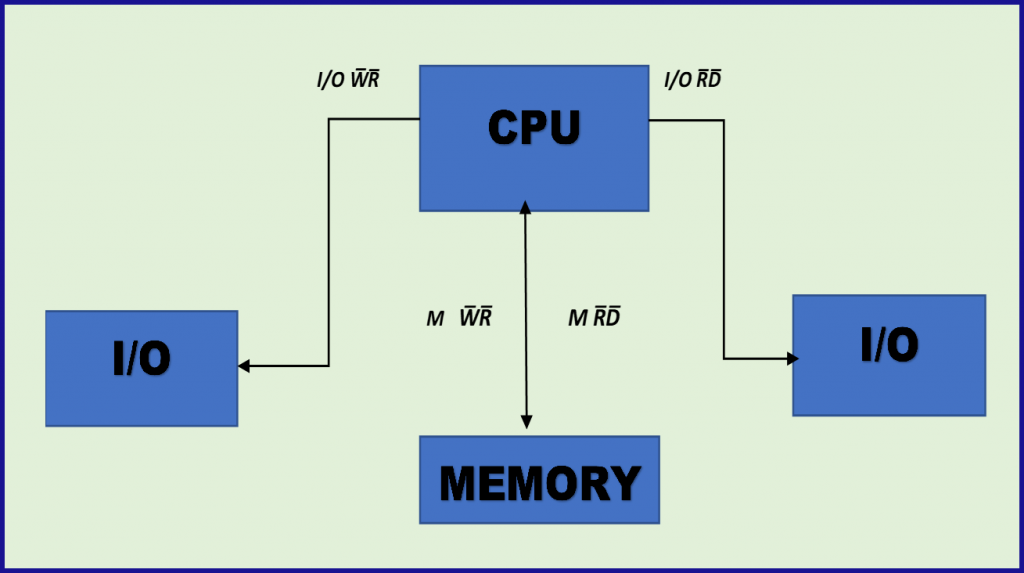
Various I/O devices & memory device are connected to a CPU by group of lines or wires, these are called BUS.

There are three categories of BUS:

ADDRESS BUS 

  • When the address is sent by CPU, all devices are connected to CPU through address BUS and receives this address but only the device will respond which also receives chip enable signal from CPU. Address BUS is Unidirectional.

DATA BUS

  •  It carries data values from microprocessor through a memory cell or a peripheral part (memory or I/O write / memory or I/O read). Data BUS is Bidirectional. So, information flows in both way between 8085 microprocessor & memory or I/O device.

CONTROL BUS

  •  It carries control signal in between Central Processing Unit, memories Input / Output devices. It is also Bidirectional.
1 2
2 3

I/O M̅When the signal is high (logic 1) then CPU wants to communicate with I/O device but when signal goes low (logic o) then CPU will communicate with memory.

R̅D̅ – When CPU sends a low R̅D̅ signal the activated device understands that CPU wants to read information from another device or memory.

W̅R̅T̅ – When CPU sends a low W̅R̅T̅ signal the activated device understands that CPU wants to write information to memory or another device.

What is OPCODE & OPERAND?

OPCODE:

An OPCODE is a signal instruction that can be executed through CPU, without help of opcode any instruction cannot be defined individually.

Example – MOV A, B

Here, MOV means Move, so MOV is OPCODE.

OPERAND:

OPERAND describes an operation such that add, sub, mov on which the operations have to be performed.

Example – MOV A, B

Here, the content of REG B moves to the content of REG A.

Read more about Important Peripherals of 8085 Microprocessor

What are the different sections of 8085 Microprocessor?

There are three categorical area in the 8085 microprocessor;

ALU:

  • This section performs the operation of subtraction, addition of logical NOR, compliment, right shifts, left shifts etc.

REGISTER:

  • Registers are used for temporary storage of data insertion; it has following register,
  • 8 BIT accumulator
  • 8 BIT General Purpose Register (B-C, D-E, H-L)
  • One 16 BIT Stack Pointer
  • One 16 BIT Program Counter
  • Instruction Reg, Status Reg, Temporary Reg

TIMING & CONTROL:

  • These is primarily responsible for the time & control signal generation which are utmost essential for completing the instruction operation. It can control the data flow between CPU & peripheral device & it provides the timing signal for the operation of memory & I/O devices.

Examples of instructions:

  • 1 BYTE Instruction – MOV B, C
  • 2 BYTE Instruction – MVI B, 05
  • 3 BYTE Instruction – LHLD 5000H

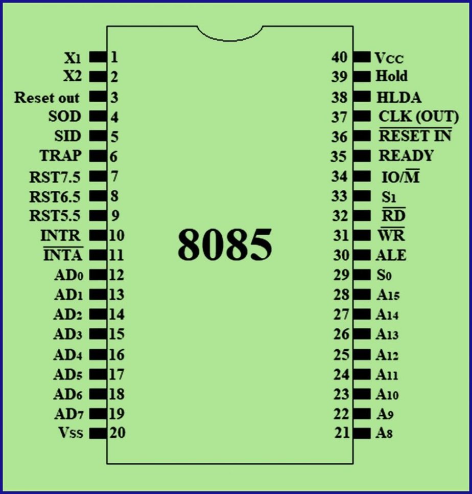
PIN Diagram of 8085 Microprocessor: 

The below image represents description of PINS of a 8085 microprocessor.

PIN Diagram of 8085 Microprocessor
PIN Descriptions of 8085 Microprocessor
I/O M̅S1S0OPERATION
000Halt
001Memory write
010Memory read
011Fetch
100Halt
101I/O write
110I/O read
111Fetch
4 2

Descriptions of the Pins of 8085 Microprocessor:

A8 – A15:

  • These address buses are used to be most significant bits of the memory address of 8 bit I/O device.

AD0 – AD7:

  • When the address is multiplexed with the data then it is called AD Bus. The lower order or low significant bus as well as the data bus are used for memory address or I/O address.

ALE

  • The ALE pin is activated for the first cycle & enable to lower 8 bit of the address data bus to be latched (logic 0) & when ALE is logic 1 then address bus is activated.
I/O M̅S1S0OPERATION
000Halt
001Memory write
010Memory read
011Fetch
100Halt
101I/O write
110I/O read
111Fetch

I/O M̅:

  • It is a status signal for memory as I/O device. When the signal goes high it operates for all I/O devices. When the signal goes low, it works for memory.

R̅D̅:

  • It is a signal to control read operation; when the signal is low then it reads the data from I/O device or O/P device.

W̅R̅T̅:

  • It is the specified write control signal. This signal specifies the data on the data bus will be written into a designated memory or I/O device.

READY:

  • It is active high I/P control signal. It is employed by µP to identify whereas a peripheral has finished the data transfer or not.

HLDA:

  • This is the hold acknowledgement signal which is used for granting the hold request.

INTERRUPT:

  • TRAP: It has the highest priority over all the interrupts. If any emergency situation comes then it will work.
  • RST 7.5: The next priority after TRAP is RST 7.5
  • RST 6.5: The next priority after RST 7.5 is RST 6.5
  • RST 5.5: The next priority after RST 6.5 is RST 5.5

INTR R:

  • It is an interrupt request used as general purpose interrupt. It has the lowest priority.

I̅N̅T̅A̅:

  • This signal is interrupt acknowledgement; is used to acknowledge all the interrupts.

RESET IN:

  • If the signal on this pin goes LOW, then the device program counter is being set to zero and when it is up it is in reset condition.

RESET OUT:

  • This signal designates the up is being reset and be utilized as to reset a memory device and input output devices.

SID:

  • Serial I/P data is the data line for signal i/p which is loaded into the accumulator’s 7th bit location.

SOD:

  • Serial o/p data is the 7th bit of the accumulator is o/p on the SOD line.

X1 – X2 [clock input]:

  • These are two input perform as a clock input.

CLOCK O/P:

  • The frequency is the same in which process operate.

VCC & GND:

  • VCC is connected to +5V; and GND pin is Grounded.

For more Electronics related article click here

Microcontroller Vs Microprocessor: 7 Facts You Must Know

1 1 300x152 1

C O N T E N T S

  • What is a Microprocessor?
  • Microprocessor Definition
  • What is BIT, BYTE, Nibble and Ward?
  • Hardware of a Microprocessor
  • Block diagram
  • Important features of Microprocessor
  • Characteristics of Microprocessor
  • What is ALU?
  • Differences between ALU and CPU
  • Memory Organization in Microprocessor
  • Types of processors used in a Microprocessor
  • Applications of Microprocessor
  • What is a Microcontroller?
  • Features of Microcontroller
  • Types of Microcontroller
  • Microcontroller vs Microprocessor

What is a Microprocessor?

Microprocessor Definition:

“Microprocessor is a programmable circuit driven register based, multipurpose semiconductor, i.e., manufactured on LSI or VLSI technique. It takes binary instructions from input devices, processes the instruction & outputs the originals and can store the information”.

Microcontroller vs Microprocessor

Hardware of a Microprocessor:

  • It is the interconnection of several peripheral in such a manner, so that it can perform a particular operation.
  • Microprocessor 8085 was found in 1976 & Microprocessor 8086 was found in 1978.

What is BIT?

The possible value of a logical variable which may or not stand for numerical digit of the binary number system is called BITs.

What is BYTE?

In binary number system a group of 8 bit are called BYTE.

                          1 BYTE = 8 BIT

What is Nibble?

A group of 4 BITS are called Nibble.

                          1 Nibble = 4 BIT

What is Ward?

An array of disk which together convey an item of information is called a Ward.

                          1 Ward = 16 BIT

                          1 Long Ward = 32 BIT

                          2 BYTE = 1 Ward

What are the features of Microprocessor 8085?

Characteristics of Microprocessor:

  • It is 40 pin IC.
  • It is NMOS technology, LSI chip.
  • Clock (CLK) speed frequency 3-5 MHz.
  • 8085 has sixteen bit (16) address lines, and eight bit (8) data lines. So, the 8085 is called an 8 bit microprocessor depending upon database.

Microcontroller vs Microprocessor

What are the limitations of microprocessor 8085?

Disadvantages of 8085:

  • Low speed.
  • Low memory capacity.
  • Limited number of GPR (General Purpose Register).
  • Less powerful instruction.

Memory Organization in Microprocessor:

Microcontroller vs Microprocessor: Memory Organisation
Microcontroller vs Microprocessor Image – 1
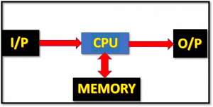
  • Microprocessor is one of the utmost key component of modern computer. It acts as a brain of computer system. A digital computing is a programmable machine. Its main components are i/p, CPU, memory, o/p device.
  • The CPU executes the instruction. The i/p device is used to fetch programme & data to the computer.
  • The memory is the storage device that stores data programme, results etc.
  • The o/p device display programmes, data or results according to their instructions given to the computer. The CPU built on a single IC which is called the MICROPROCESSOR.
  • A digital device in which microprocessor is in case to operate as a CPU is known as MICROCONTROLLER.

Microcontroller vs Microprocessor

Microprocessor Applications:

Microprocessors are widely used in-

  • Different household devices like thermostats, high end coffee makers, washing machines etc.
  • Microprocessor has various industrial applications like cars, boats, heavy machinery, elevators etc.
  • In cell phones, VCR, televisions microprocessor is used numerously.

Types of Microprocessor:

16 BIT Microprocessors-

  • 8086 (Clk speed 4.7 MHz – 10 MHZ);
  • 8088 (Clk speed more than 5 MHz);
  • 80186,80188 (Clk speed 6 MHz);
  • 80286 (Clk speed 8 MHZ);

32 BIT Microprocessors-

  • INTEL 80386 (clk speed 16 MHZ – 33 MHz);
  • INTEL 80486 (clk speed 16 MHz – 100 MHZ);
  • PENIUM (clk speed 66 MHz);

64 BIT Microprocessor-

  • INTEL CORE-2 (clk speed 1.2 GHz – 3 GHz);
  • INTEL i7 (clk speed 3.3 GHz – 66 GHz);
  • INTEL i5 (clk speed 2.4 GHz – 3.6 GHz);
  • INTEL i3 (2.93 GHz – 3.33 GHz);
Microcontroller vs Microprocessor
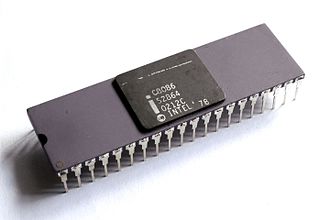
Intel C8086 processor , Microcontroller vs Microprocessor, Image – 2
Photo By – Thomas NguyenIntel C8086CC BY-SA 4.0

Types of processors used in a Microprocessor:

Reduced Instruction Set Computer (RISC) –

An advanced processor circuit consists of RISC architecture. RISC provides improved performance. A RISC has a few addressing modes only. It executes most instructions in a single clock style. Instruction executes by a hardwired implementation. Arithmetic & logic instructions access the operands in multiple register sets, windows or files. This greatly reduces dependency on the external memory accesses for the data.

Complex Instruction Set Computer (CISC) –

CISC has the ability to process complex instructions and complexioned data sets with the smaller number registers and simpler hardwired logic, and use of control memory. CISC be responsible for for a large number of address mode.

CISC may have the addressing modes such as indirect, auto index, index relative addressing modes for the data transfer, logic and arithmetic instructions. Some CISC have reliance on the external memory admittances for data in several addressing modes.

What is ALU?

In computing system, the ALU is a digital circuitry which can perform various mathematical operations.


Differences between ALU and CPU:

 Arithmetic Logic Unit (ALU)Central Processing Unit (CPU)
Full FormALU is the Arithmetic Logic Unit.CPU is Central Processing Unit.
UseALU performs all the arithmetic operations specified to the computer.CPU carries different instructions of a computer program to compute different processes i.e., arithmetic, logical, control & input output operations.
DependenceALU depends on the central unit for the for its functionThe control unit does not depend on anything like ALU.
FunctionsALU takes instructions from control unit and gives result accordingly.Control unit provides instruction to the arithmetic unit to perform.
Microcontroller vs Microprocessor, Table -1

What is a Microcontroller?

Definition of Microcontroller:

“A microcontroller is a device which is made up of microprocessor, Random Access Memory, Read Only Memory, timer, input-output pins and several other device.”

Features of Microcontroller:

Different units of Microcontroller (8051):

  • It has a 12 MHz clock, processor instruction cycle time is 1µs.
  • Microcontroller 8051 has 8 bit arithmetic logic unit.
  • Its internal bus width is 8-bit.
  • It has CISC architecture.
  • Microcontroller 8051 also equipped with a stack pointer.
  • The 8051 equipped with two external interrupt pins, INT0 & INT1.
  • Special Function Register is present in the 8051 microcontroller family.

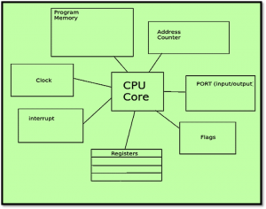
Block Diagram of Microcontroller:

Microcontroller vs Microprocessor
Microcontroller vs Microprocessor, Image – 3

Types of Microcontroller:

  • PIC Microcontroller;
  • ARM Microcontroller;
  • 8051 Microcontroller;
  • AVR Microcontroller;
  • MSP Microcontroller;
Microcontroller vs Microprocessor
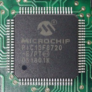
A PIC Microcontroller, Microcontroller vs Microprocessor, Image – 4

Applications of Microcontroller:

Microcontrollers are used widely in-

  • Mobile phones
  • Automobile Industry
  • Cameras
  • Computer Systems
  • Micro Oven etc.

Comparative analysis between Microprocessor and Microcontroller:

Microcontroller vs Microprocessor

     MICROPROCESSOR    MICROCONTROLLER
CPUIt consists of only one CPU.  It consists of a CPU along with memory, I/O all integrated into one chip.
USEMicroprocessor is used in personal computers.Microprocessors are typically used in any of the computational devices or remote controlled systems.
INTERFACEMicroprocessor interfaces are complex.Microcontrollers are straight forward with fewer instructions to execute.
COSTThey are expensiveThey are inexpensive
REGISTERIt has fewer number of register and the operation in it is mainly based on the memory.Here Registers are greater in number. That is why it is more convenient to write programs.
Microcontroller vs Microprocessor, Table – 2


For more Electronics related article click here

UFT Tutorial:Create Test Case–Step By Step Guide For UFT 14.x

Create Test Case in UFT Folder Structure 300x100 1

Software testing is become the most important phase in software development life cycle which ensures the quality of end product. So, with out the successful testing phase, it will be extremely risky to deploy the software product in the production. In today’s busy life, market demands a faster releases of software product with high quality. Here, is come into the picture to reduce the testing cycle with expected quality. There is lots of automation tools are available in the market, but Unified Functional testing (UFT) tool is playing as the key player in software testing domain.

In this Create Test Case in UFT article, we are going to learn about the step by step guidance to create the test case in UFT along with the test framework.

UFT Tutorial – Table of Content

UFT Tutorial #1: UFT Overview

UFT Tutorial #2: UFT Setup – Download, Install, License Configuration and ALM Connection

UFT Tutorial #3: UFT Object Repository

UFT Tutorial #4: UFT Actions & Function Library 

UFT Tutorial #5: UFT Parameterization 

UFT Tutorial #6: VB Scripting in UFT

UFT Tutorial #7: Step by Step Guide to Create Test Case in UFT

UFT Tutorial #8: Exception Handling in UFT

UFT Tutorial #9: Recording in UFT with Checkpoints & Dictionary Object 

UFT Tutorial #10: UFT Interview Questions and Answers 

Step by Step Guide to Create Test Case in UFT

UFT is the short form of Unified Functional Testing, which is previously known as Quick Test Professional (QTP). With the help of VB Scripting, test cases build to automate any functional testing scenario.  Here, we are automating a sample application using the tool UFT. We are trying to explain each of the steps to automate the test scenario. First, we will understand the functional scenario which will be automated later in this article –

Functional Test Scenario:

Test Case Summary: Book flights through sample Flights Application.

Step#DescriptionExpected Result
1Open the Flights App (FlightsGUI.exe)The login screen should appear.
2Login with a valid credential (Username- John, Password- HP)Book Flight Screen Should appear.
3Enter below criteria and click on Find Details –  Source: Frankfurt  Destination: Portland  Travel Date: Today + 2 days  Class: Business  Tickets: 1A list of flights available should be displayed.
4Select the first available option and click on the button, “SELECT FLIGHT.”Flight Details screen should appear.
5Enter passenger name and click on “Order” button.A confirmation message with the Order Number should appear.
6Close the application.The application should disappear.

Test Automation Approach:

After analyzing the scenario, we can assume that the application having one major flow, i.e., flight booking, and this flow is applicable for different sets of test data. So, we will follow the below test automation approach to automate this particular scenario.

Framework Identification: Hybrid Framework which will be a combination of data-driven and modular automation test frameworks.

Environment variables: We need to store the configuration information such as application details, user credentials, framework path, etc., in external environment variables.

Test data: In a data-driven approach, we will store the data in the external excel sheet, which will be imported in the test case.

Object Repository: Create a central repository of test objects (i.e. shared object repository) so that multiple test cases can refer it to increase the reusability.

Reusables/Modules: We will create functions as modules to break the scenario into small parts.

Create Testcase in UFT – Step by Step Guide:

Step1 – Folder Structure: 

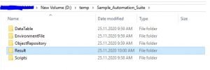
Below folder structure need to be created to set up the data driven automation test frameworks. The required folders are – 

Scripts  – UFT test cases will be stored here.

DataTable – It’s used to store the test Datasheets.

EnvirnmentFile – External Environment variable(xml) files are kept here.

ObjectRepository – The shared object repository (.tsr file) will be kept here.

The result – Result related files can be stored here.

Library – Function libraries will be stored here.

Create Test Case in UFT - Folder Structure
Create Test Case in UFT – Folder Structure

Step2 – Create XML for External Environment Variables: 

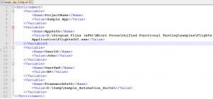
All the configuration or user-related data that are applicable for the entire automation suite need to be kept in an external environment file(XML) so that same can apply to the entire suite. Which needs to be stored in the EnvironmentFile folder. Here below parameters are created – 

ProjectName – It will be used for reporting purposes.

AppPath – The application exe path is stored here.

UserId/UserPwd – Refer to the application credential.

FrameworkPath – Refer to the root path of the test framework’s folder structure.

Create Test Case in UFT - External Environment Variable
Create Test Case in UFT – External Environment Variable

Step3 – Create External Data Sheet:

All the required test data will be store in an external excel file (FlightbookingData.xlsx), which needs to be stored in the DataTable folder. In this excel, column A, i.e., “TestCaseID,” will be used to map the data row with the current test case. 

Create Test Case in UFT - Shared Object Repository
Shared Object Repository (Create Test Case in UFT )

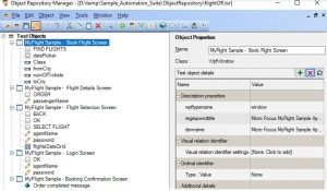
Step4 – Create/Modify Shared Object repository:

· Open the UFT component “Object Repository Manager” to create shared repository..

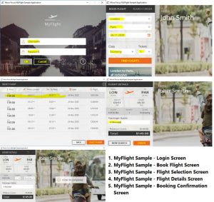
· Navigate Each of the application screens, as shown below images.

· Add the required test objects into this newly created shared object repository.

· The object repository is created now. Now we need to save the shared object repository in the ObjectRepository folder with the “TSR” extension.

Create Test Case in UFT - Application Overview
Create Test Case in UFT – Application Overview
Create Test Case in UFT - Shared Object Repository
Create Test Case in UFT – Shared Object Repository

Step5 – Create reusables:

Below functions need to be created in a function library which will store in Library folder with qfl extension,

ImportSheetAndSelectRow – Import Datasheet and Select Desire Data Row

OpenApp – Open Application

LoginToApp – Login to the Application

EnterDetailsToFindFlight – Enter details to find flights.

SelectFlight – Select a row to book the flight.

EnterPassengerNameAndOrder – Book the flight and verify the success message.

CloseApp – Close the application.

Create Test Case in UFT - Function Library 1
Create Test Case in UFT – Function Library 1
Create Test Case in UFT - Function Library 2
Create Test Case in UFT – Function Library 2

Step6 – Create Testcase in UFT:

Now we need to create the empty test case in uft and link the external resources. It should be created in the Scripts folder. After the creation of the test case, the external environment XML shared object repository and function library has to be attached with the test case.

Create Test Case in UFT - Associates with External Components
Create Test Case in UFT – Associates with External Components

Step7 – Call the modules:

Now we need to call the reusable modules, stored in the function library, in the local action(based on the test functionality) to complete the development. After this step, the test case will be complete from the automation point of view.

Create Test Case in UFT - Automated Test Case
Create Test Case in UFT – Automated Test Case

Step8 – Perform dry run and check the reports:

No need to execute the test case once to check if the scripts are working as expected. We can perform this check by reviewing the below reports. 

Create Test Case in UFT - Dry Run Result
Create Test Case in UFT – Dry Run Result

Here, based on the logs displayed in the report, we can assume that the test case has been developed correctly.

Conclusion:

In this Create Test Case in UFT article, we have learned about step by step approach to develop the test framework and create a test case in UFT. Please click here to get more information on this topic from the Microfocus support portal.
VB Scripting in UFT–An Excellent Guide for Beginners

VB Scripting in UFT If Else Conditional Statements in UFT 300x124 1

Testing is now the most essential phase in software development process to ensure the quality of the product. Also, without having testing, it will be very risky to release the software to use. The test automation process has changed the testing dimension with respect to effort savings and lightning fast regression cycle. There is many test automation tools are used in the testing industry. But, the most used automation testing tool is UFT.  

In this VB Scripting in UFT article, below topics will be explained with examples –

· Variables in UFT

· Constants in UFT

· Array in UFT

· Conditional Statements in UFT

· Looping Statements in UFT

· Sub and Function Procedures in UFT

UFT Tutorial – Table of Content

UFT Tutorial #1: UFT Overview

UFT Tutorial #2: UFT Setup – Download, Install, License Configuration and ALM Connection

UFT Tutorial #3: UFT Object Repository

UFT Tutorial #4: UFT Actions & Function Library 

UFT Tutorial #5: UFT Parameterization 

UFT Tutorial #6: VB Scripting in UFT

UFT Tutorial #7: Step by Step Guide to Create Test Case in UFT

UFT Tutorial #8: Exception Handling in UFT

UFT Tutorial #9: Recording in UFT with Checkpoints & Dictionary Object 

UFT Tutorial #10: UFT Interview Questions and Answers 

UFT Tutorial #4: VB Scripting in UFT

VB Scripting in UFT:

UFT supports VB Scripting as the programming language to write the code for any test cases. VB Script is derived from Visual Basic 4.0 language, which was developed by Microsoft. VB Scripting in UFT is very easy to learn, and it can be used to develop both server-side and client-side scripting.

Variables in UFT:

Variables in UFT are the placeholder that denotes a memory location that stores program information. It can be changed during run time. A variable has been represented by its name to read/write the stored value. Only one type of variant is available in VB Scripting, which can interact with numbers, strings, or dates. Based on the data, the variable is acted accordingly.

If we store any number with the double quotation, then it’s acted as a string type variable. VBScript in UFT allows us to declare the variables with the help of below three statements –

  • Dim
  • Public
  • Private

Dim Statement – Dim is used to declare any variable immediately irrespective of the datatype. One dim statements allows to declare multiple variables which are separated by comma. The scope of this type of variable is within the code block( in the Case of UFT, scope is restricted to the corresponding actions or function or sub).

Dim myVariable

 Dim myVariable1, myVariable2, myVariable3

We can declare any variable immediately by using its name in the code. So, in this case, an additional declaration statement is not required. But, if we keep the statement “Option Explicit” at the beginning of our scripting area, we have to write the variable declaration statement. Otherwise, UFT will throw an error message.

Public statement – If we declare variables as public, the variables are available throughout all the scripts in the suite.

Private statement – If we declare variables as private, variables are available within the script itself.

Assigning Values to Variables:

Using the below structure, we can assign values to the variables using the equal symbole – 

variableNameString = “My Value” //Assign string

variableNameNumber = 1234 //Assign number

Here variable name should be kept on the left side of the equal symbol, where the value should be kept on the right side. For String, the value should be kept within double quote marks.

Scalar Variables – When we store a single value to the variable, it’s represented as Scalar Variable.

Array Variables – When string more than one value in a single variable, it is known an array. We declare an Array Variable with a parenthesis. In the below example, a single-dimension array containing six elements is declared:

Dim myArrayStudents(5)

Here index starts from 0 to 5, so the records will always be one more than the number shown in parenthesis. Value assignments are done in the below way –

myArrayStudents(0) = “Vikram”

myArrayStudents(1) = “Tom”

.

.

myArrayStudents(5) = “Jerry”

Naming Convention:

The standards rule for the naming convention are mentioned below – 

  • It should begin with an alphabetic character.
  • It should not contain an embedded period.
  • Name should be self explanatory.
  • The maximum length should not be exceeds 255 chars.

Constants in UFT:

We can consider a constant as a variable of a number or String whose value will never change. i.e., after defining a constant, it will be acted as a read-only place holder. The VBScript already provides many in build constants variables like , vbOK, vbTrue, vbFalse, vbCancel, and so on. A constant has to be declared and defined using the keyword “CONST” like the below example –

Const MyString = “This is my string.”

Const MyAge = 49

 Within modules, constants are always private, and visibility can not be changed.

Array in UFT:

Array in UFT is a variable that stores a collection of values having the same data type such as number, String, etc. A set of same type elements can be stored in the same memory location where each of the element can be accessed by their reference number which are known as array index. The index of the first element always start from zero value.

While declaring an array we need to define two parts – the logical name of the array and the array subscripts which indicates the highest value of array index. Array indexes are the unique numbers which represent the each element of that array. This index always starts from zero.

It should be declared before use. We can declare an array by the dim statement. Two types of arrays are available in UFT –

·        Local Array – The scope of local array is restricted to the current function or procedure block where it was declared.

·        Global Array – If the array is declared globally or at the start of script, the values of the array (i.e. scope) can be accessed from all the functions or procedures which are defined with in the same vbscript.

Static and Dynamic Arrays:

VBScript allows us to declare static or dynamic array in UFT.

A static array can not be modified during the uft regression. It means, the static array keeps defined number of elements through out the execution.

A dynamic array can be enhanced at any point of time during the test execution.

Declare and assign Values to Arrays:

Declaration statements – Dim myArray(subscriptvalue)

Example: Declaring an array which stores four students name and assigns the value in it.

Dim arrStudents(3)

arrStudents(0) = “Tom”

 arrStudents (1) = “Henry”

arrStudents (2) = “Tina”

arrStudents (3) = “Vicky”

Conditional Statements in UFT:

The conditional statements are most important features of scripting to make it flexible and robust. The mostly used conditional statement in UFT will be explained through out this section.

If-Else Statement:

The If – Else statement is used build the conditional log in the UFT script. The purpose of this statement is to check one or multiple conditions and perform certain activities based on the checking. For an example – Here we will identify the current week day using the if-then-else statement.

If-Else Conditional Statements in UFT

The multiple elseif statements can be used to check multiple conditions. Also, we can write multiple conditions in the first line of “if statement” which should be separated by logical operators such as OR, NOT, AND, etc.

Select Case Statement / Switch Case Statement:

It is an alternative approach of instead of using multiple if conditions for a single variable. 

The Select-case statement is very helpful for the scenario where based on the different values of a single variable, we need to perform different activities. It’s also know is switch-case-statement. The use of case statement, we can write our script in a organized way. The select case statement execute the conditional expression at the beginning and the result of the conditional expression, will matched with different static conditions in case statement. Here, only the associated steps will be executed for the match case.

For an example – Here we will identify the current week day using the select case statement.

Select - Case Conditional Statements in UFT
Select – Case Conditional Statements in UFT (VB Scripting)

Looping Statements in UFT:

In a situation, where similar codes are executed again and again based on some conditions, it is advisable to use looping statements for better readability and efficiency . In this section, we will discuss about the different kinds of loops with the examples, which are very helpful in UFT scripting. The loops work on conditions or maximum iteration counters. The frequently used looping statements in UFT are explained below –

· Do Loop Statement

· While Loop Satement

· For Loop Statement

Do Loop:

When we need to execute few steps repeatedly based on one or multiple conditions, we need to use the Do Loop statements as it allows to continue the looping based on conditions. The loop will be continued till the conditions are getting satisfied. Here, the conditions are checked at the end of the looping statement. That means, the first iteration is always executed irrespective of the condition checking result. To exit from the middle of the loop for another specific if condition, the “Exit Do” statement can be used. At end of the loop, “while” statement is used for conditional checking. Example – In this example, the loop will be continued, until the counter value reached to 10,

VB Scripting in UFT - Looping Statements in UFT (Do-Loop)
VB Scripting in UFT – Looping Statements in UFT (Do-Loop)

It’s similar to Do-Loop structure. When we need to execute few steps repeatedly based on one or multiple conditions, we can use the While Loop statements as it allows to continue the looping based on conditions. The loop will be continued till the conditions are getting satisfied. Here, the conditions are placed at the beginning of the loop with the help of while keyword. That means, none of the iteration will be executed if the checking of the conditions are failed. To exit from the middle of the loop for another specific if condition, the “Exit While” statement can be used. At beginning of the loop, “while” statement is used for conditional checking. The primary difference between Do-Loop and While-Wend statement is the place of condition checking.

Example – In this example of VB Scripting, the loop will be continued, until the counter value reached to 10,

VB Scripting in UFT -Looping Statements in UFT (While-Wend)
While-Wend Looping Statements in UFT (VB Scripting in UFT)

For Loop:

For– Next statements are defined predefined iteration counter. The loop will be continued till the counter reached the highest value which is specified with “for” keyword. To exit from the middle of the loop for another specific if condition, the “Exit For” statement can be used. At end of the loop, “while” statement is used for conditional checking.

Example – In this example, the loop will be continued for ten iterations,

VB Scripting in UFT - Looping Statements in UFT (For-Next)
VB Scripting in UFT – Looping Statements in UFT (For-Next)

Sub Procedure in UFT:

A sub procedure in UFT is a group of statements which are bounded by the keyword “Sub” and “End Sub” to perform a specific task. It does not return any value. We can pass values to sub procedure as arguments. An empty parenthesis() represents that there is not input arguments. In UFT, the sub is used to create a unit of the functional block for modularization. 

For example, the below code shows that a sub is used to calculate and display the interest value based on the input interest rate, years, and principal amount.

VB Scripting in UFT - Sub Procedure in UFT
VB Scripting in UFT – Sub Procedure in UFT

Function Procedure in UFT:

A function procedure in UFT is a group of statements which are bounded by the keyword “Function” and “End Function” to perform specific activity and return the output. A function procedure in UFT is a block of statements enclosed by Function and End Function statements to perform specific actions. It has the data return capabilities, which is the primary difference with a sub. We can pass values to function procedure as arguments. We need to include an empty parenthesis() when no argument is required. In UFT, Function is used to create a unit of the functional block for modularization. 

For example, the below code shows that a Function is used to calculate and display the interest value based on the input interest rate, years, and principal amount.

VB Scripting in UFT - Function Procedure in UFT
VB Scripting in UFT – Function Procedure in UFT

Conclusion:

In this VB Scripting in UFT article (UFT Tutorial), we have learned about different variables, constants, arrays, conditional and looping statements. Click here to learn more on VB Scripting. Also, if you want to prepare for UFT Interview Questions, please click here.

Laser Cladding Process: 5 Important Uses and Advantages

laser cladding process 5 important uses advantages

Laser cladding is a versatile and advanced surface engineering technique that has gained significant attention in various industries due to its ability to enhance the performance and durability of components. This process involves the deposition of a thin layer of material, typically a metal alloy or a composite, onto a substrate using a high-energy laser beam. The laser cladding process offers numerous advantages and has various important uses, making it a valuable tool in the field of materials science and engineering.

1. Precision and Accuracy

Laser cladding provides exceptional precision and accuracy in depositing materials, allowing for the creation of intricate geometries and the application of customized coatings with specific properties. This is achieved through the precise control of the laser beam, which can be focused to a small spot size, typically ranging from 2 to 6 mm in diameter. The laser beam’s high energy density, typically in the range of 10^6 to 10^8 W/cm^2, enables the rapid melting and solidification of the cladding material, resulting in a well-defined and uniform clad layer.

The accuracy of the laser cladding process is further enhanced by the use of computer-controlled positioning systems, which allow for the precise movement of the laser beam or the workpiece. This precision enables the creation of complex shapes and the application of coatings with intricate patterns, making it an ideal choice for applications that require high-quality surface finishes, such as in the aerospace, automotive, and medical industries.

2. Minimized Distortion and Improved Bonding

laser cladding process 5 important uses advantages

The high-energy lasers used in the laser cladding process minimize distortion and improve the metallurgical bonding between the substrate and the cladding material. This is due to the precise control over the heat input, which reduces thermal damage and enhances the quality of the cladding.
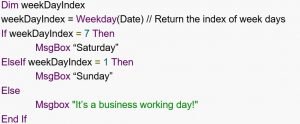
The laser cladding process typically involves the use of a focused laser beam to melt a thin layer of the cladding material, which is then deposited onto the substrate. The rapid heating and cooling cycles associated with this process result in a localized and controlled heat input, minimizing the overall thermal distortion of the workpiece. This is in contrast to other cladding techniques, such as arc cladding, which can introduce significant thermal distortion due to the higher heat input.

The improved metallurgical bonding between the substrate and the cladding material is achieved through the formation of a strong metallurgical interface. During the laser cladding process, the cladding material and the substrate material undergo partial melting and intermixing, creating a well-defined and cohesive bond. This enhanced bonding strength helps to prevent delamination or spalling of the cladding layer, improving the overall durability and performance of the coated component.

3. Versatility in Material Selection

Laser cladding is compatible with a wide range of materials, including metals, alloys, ceramics, and composite materials. This versatility enables the use of optimal materials for specific applications, enhancing the performance and durability of the cladded components.

The choice of cladding material is crucial in determining the properties of the final coated component. Metals and alloys, such as stainless steel, cobalt-based alloys, and nickel-based superalloys, are commonly used in laser cladding for their superior wear resistance, corrosion resistance, and high-temperature performance. Ceramic materials, such as tungsten carbide and chromium carbide, can be incorporated into the cladding layer to improve hardness, wear resistance, and thermal barrier properties.

Furthermore, the laser cladding process allows for the deposition of composite materials, which can combine the desirable properties of different constituents. For example, a metal matrix composite (MMC) consisting of a metal alloy reinforced with ceramic particles can be deposited using laser cladding, resulting in a coating with enhanced wear resistance, thermal conductivity, or specific functional properties.

The ability to tailor the cladding material to the specific requirements of the application is a significant advantage of the laser cladding process, making it a versatile and adaptable technology for a wide range of industries.

4. Reduced Thermal Distortion and Heat-Affected Zone

Laser cladding inputs less than 20% of the heat compared to arc cladding the same part, resulting in greatly reduced thermal distortion and a smaller heat-affected zone. This minimizes the need for follow-up operations like machining and straightening, and increases the strength of the part.

The laser cladding process is characterized by a highly localized and controlled heat input, which is a key factor in minimizing thermal distortion. The focused laser beam melts only a thin layer of the cladding material and the substrate, resulting in a rapid heating and cooling cycle. This rapid thermal cycle limits the extent of the heat-affected zone (HAZ) and reduces the overall thermal distortion of the workpiece.

In contrast, traditional cladding techniques, such as arc cladding, typically involve a higher heat input, which can lead to significant thermal distortion and a larger HAZ. The larger HAZ in arc cladding can result in microstructural changes and residual stresses in the substrate material, potentially compromising the mechanical properties of the component.

The reduced thermal distortion and smaller HAZ in laser cladding minimize the need for post-processing operations, such as machining and straightening, which can be time-consuming and costly. Additionally, the increased strength of the part due to the reduced thermal distortion can enhance the overall performance and reliability of the coated component.

5. Better Layer Thickness Control and Surface Finish

Laser cladding offers better control of layer thickness, the ability to apply thinner clad layers, and improved surface finishes. This reduces the amount of finish machining required and results in a more near net shape coating, reducing excess clad material and improving the overall efficiency of the process.

The precise control over the laser beam parameters, such as power, scan speed, and powder feed rate, allows for the deposition of cladding layers with a high degree of thickness control. This enables the application of thin, uniform cladding layers, typically ranging from 0.5 to 3 mm in thickness, without compromising the quality or the metallurgical bonding of the coating.
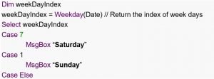
The ability to apply thinner cladding layers is advantageous for several reasons. Firstly, it reduces the amount of excess cladding material that needs to be removed through post-processing operations, such as machining or grinding. This, in turn, improves the overall efficiency of the process and reduces material waste. Secondly, the thinner cladding layers result in a more near net shape coating, which can minimize the need for extensive finish machining and reduce the overall manufacturing time and costs.

Furthermore, the laser cladding process can produce coatings with improved surface finishes, typically in the range of 1 to 5 μm Ra (average roughness). This is achieved through the precise control of the laser beam parameters and the optimization of the powder characteristics, such as particle size and distribution. The improved surface finish reduces the need for additional polishing or grinding operations, further enhancing the efficiency and cost-effectiveness of the laser cladding process.

In summary, the laser cladding process offers numerous advantages, including precision and accuracy, minimized distortion and improved bonding, versatility in material selection, reduced thermal distortion and heat-affected zone, and better layer thickness control and surface finish. These advantages make laser cladding a valuable tool in various industries, such as aerospace, automotive, energy, and medical, where the enhancement of component performance and durability is of paramount importance.

References:
1. Toyserkani, E., Khajepour, A., & Corbin, S. (2005). Laser cladding. CRC press.
2. Dutta Majumdar, J., & Manna, I. (2011). Laser material processing. International materials reviews, 56(5-6), 341-388.
3. Zheng, B., Zhou, Y., Smugeresky, J. E., Schoenung, J. M., & Lavernia, E. J. (2008). Thermal behavior and microstructure evolution during laser deposition with laser-engineered net shaping: part I. numerical calculations. Metallurgical and Materials Transactions A, 39(9), 2228-2236.
4. Gu, D. D., Meiners, W., Wissenbach, K., & Poprawe, R. (2012). Laser additive manufacturing of metallic components: materials, processes, and mechanisms. International materials reviews, 57(3), 133-164.
5. Toyserkani, E., Khajepour, A., & Corbin, S. (2004). 3-D finite element modeling of laser cladding by powder injection: effects of laser pulse shaping on the process. Optics and Lasers in Engineering, 41(6), 849-867.