Topics for Discussion
A. Xilinx
B. Prerequisites for Verilog HDL Using Xilinx
C. Xilinx Installation process
D. Creating your first Verilog project with XILINX
XILINX
Xilinx is a USA based tech-company which provides programmable logic devices. We will use Xilinx’s software “ISE 14.7 Simulator to implement Verilog designs. Xilinx is also used for VHDL implementations. Though some of the coding structure of Verilog is same as VHDL, there are fundamental differences between them.
First of all learn Verilog! Click Here!
Prerequisites for Verilog using Xilinx
Before getting started with Verilog with Xilinx, there are some prerequisites for an user. They are listed below.
- Must have some knowledge of digital electronics. At least bits of knowledge of basic logic gates and sequential circuits are required.
- An uninterrupted internet connection is a must.
- A healthy amount of free memory is required to run the software smoothly. At least 20 GB space is needed in your machine.
- Create an account on Xilinx’s website with an accessible email-id. The license will be mailed in that email-id.
- We are demonstrating this tutorial for windows only.
What is VHDL? What is the difference between Verilog & VHDL?
Xilinx Installation Process
- Step 1: Download the software from the internet. The link to download Xilinx is given below –
(It is a 6GB ZIP file, ensure internet connection and space) The link for windows –
https://www.xilinx.com/member/forms/download/xef.html?filename=Xilinx_ISE_DS_Win_14.7_1015_1.tar
There are other downloadable options available. You can choose according to your requirement and choice from the below given link.
- Step 2: Unzip the file. To unzip the file, right-click on the file, and there will be an option to extract all. After the extraction, the file name should be – ‘Xilinx_ISE_DS_Win_14.7_1015.1”.
Point to be noted – Both the download and extraction will need a lot of time depending upon internet speed and storage availability. The installation will require a lot of time too. So, don’t panic, be patient.
- Step 3: Open the extracted file. There is a file named – ‘xsetup’. Double click on that file. It will start the installation.
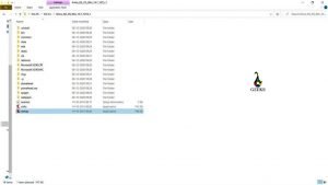
- There will be another pop-up, choose the ‘ISE WebPACK’ option to continue.

It will start the final installation process.
- Step 4: After the software gets installed in your PC, some tasks must be performed. Do these tasks carefully. Also, update the license from Xilinx. Those steps are given in the previous article; please check it out before we start with our first Verilog Project. The link is given below.
https://lambdageeks.com/vhdl-process-xilinx-guide/
Creating your first Verilog project with XILINX
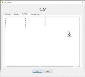
We will first implement a simple AND gate model using XILINX. The logical representation of AND gate is Y = AB; A and B are the two inputs, while Y is the output. The truth table is given below.
| A | B | Y =AB |
| 0 | 0 | 0 |
| 0 | 1 | 0 |
| 1 | 0 | 0 |
| 1 | 1 | 1 |
- Step 1: Open the project navigator by double clicking the icon on the desktop.
- Step 2: Go to ‘File’ and then ‘New Project’. File -> New Project

- Step 3: Type a name for your project and select the storage location. It is advised not to use basic logic gate names as they are reversed keywords. Also, don’t forget to copy the name of your project; it will help your letter. Click on the ‘Next’ button to proceed.
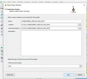
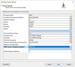
- Step 4: Now, you have to set up a few things. Be careful while setting up all these things. Any mistake will lead to failure in the long-term result.
- Property Name: Value
- Evaluation Development Board: None Specified
- Product Category: All
- Family: Spartan3
- Device: XC3S50
- Package: PQ208
- Speed: -4
- Top Source Type: HDL
- Synthesis Tool: XST (VHDL/Verilog)
- Simulator: lSim (VHDL/Verilog)
- Preferred Language: Verilog
- Property Specification in Project File: Store all values
- Manual Compile Order: Leave the checkbox, don’t click on it.
- VHDL Source Analysis Standard: VHDL-93
- Enable Message Filtering: Leave the checkbox, don’t click on it.
Click on ‘Next’ to proceed.
- Step 5: Now, click on ‘Finish; for the next pop-up.
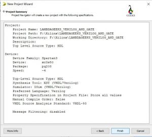
- Step 6: A new window will be opened up in the ISE simulator. Inside the design tab at the left corner, and under the Hierarchy bar, the model will have appeared. Move your cursor on the folder just below the named model.
Then right-click on the folder (in our case the name of the folder is – ‘xc3s50-4pq208’). Then, select the new source.

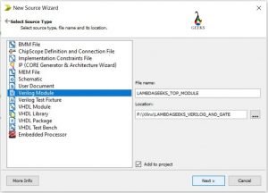
- Step 7: In the new window, choose the ‘Verilog Module’ and paste the same name you have copied in the step 3. You can also get that name from the location tab. Click on ‘Next’ to proceed.
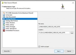
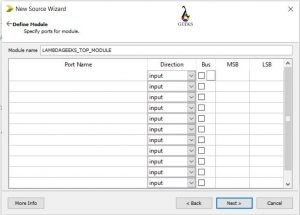
- Step 8: The defining module will come up. But we will not define the ports now. Just click on ‘Next’.
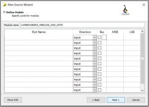
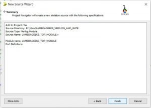
- Step 9: Click on “Finish” for the next window pop-up.
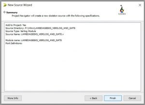
- Step 10: A code editor will be opened up.
- Now change the project name written in the editor to “AND”. For our case, we change it from ‘LAMBDAGEEKS_VERILOG_AND_GATE’ to ‘AND’.

- Now write down the port declarations as follow.
module AND (
input I1, I2,
output O
);
endmodule
- Now assign the AND gate in-between the input and output.
assign O = I1 & I2;

- Save the code.
- Step 11: Now, on the left side of the window, under the design bar, you can see a tab named “Process AND”.
- Expand the ‘Synthesis – XST’ from there.
- Double click on the ‘Check Syntax’. It will show a green tick, denoting success.
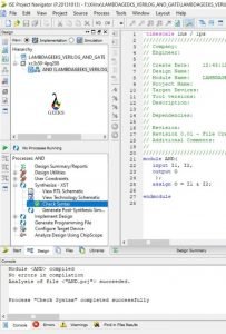
- Step 12: Now again go back to the top-left section. Right-click on the ‘xc3s50-4pq208’ file. Choose a new source from there.
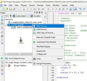
- Step 13: Choose Verilog Module from the given list. Then put a file name. We put “LAMBDAGEEKS_TOP_MODULE” as the name. Click on the ‘Next’ to proceed.
- A pop-up named ‘Define Module’ will come. Do not define anything here. Click on the ‘Next’.
- Click on ‘Finish’ for the next popped-up window.
- Step 14: A code editor will be opened up. You can erase all the comment section from the code editor.
- Now, check the Hierarchy Section at the top left. Right-click on the Module Name given by you. For our case, it is – ‘LAMBDAGEEKS_TOP_MODULE’.
- Some options will come upon the right click. Choose the option – ‘Set as Top Module’.
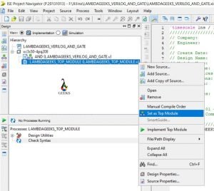
- A window will pop-up. Click on ‘YES’ to continue.

- Step 15: Now, we have to write some code using the code editor. It describes the input and output with the gate implementation. The following code is written for AND gate –
module LAMBDAGEEKS_TOP_MODULE(
input I1, I2,
output O
);
AND and1(I1,I2,O);
endmodule

- Step 16: Now go to the left down part at ‘Process: LAMBDAGEEKS_TOP_MODULE’ section.
- Now Expand the ‘Synthesis -XST’ part.
- Double click on the ‘Check Syntax’. It will show a green tick denoting success after a few seconds.
- Then, Double click on the ‘Synthesis – XST’ option. It will take a few seconds to show a green tick.
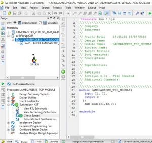
- Step 17: View for RTL Schematic.
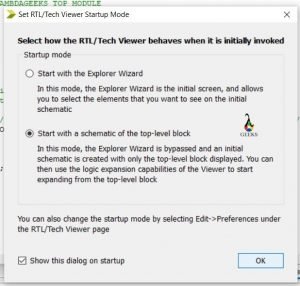
- Double click on the ‘View RTL Schematic’ option.
- A window named – ‘Set RTL/ Tech Viewer behaves when it is initially invoked’ will pop up. Just click on the ‘OK’.
- Now a window will be opened with a diagram.
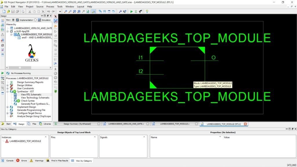
- Double click inside the box.

- Now, double click inside the AND box.
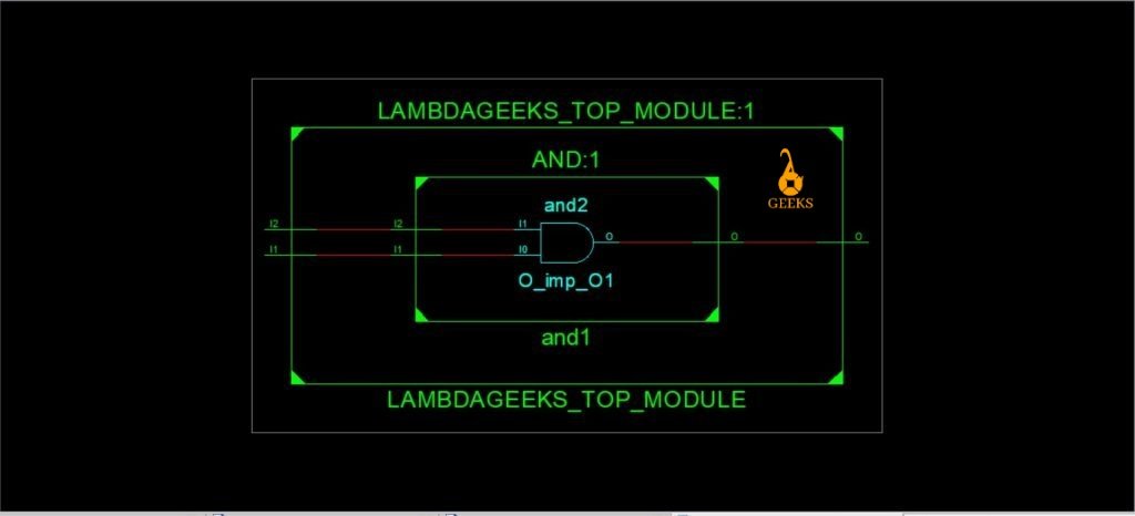
- Step 18: View for Technology Schema
- Double click on the ‘View technology Schematic’ option.
- A pop-up will come to click on the ‘OK’ option.
- A new diagrammatic window opened up.
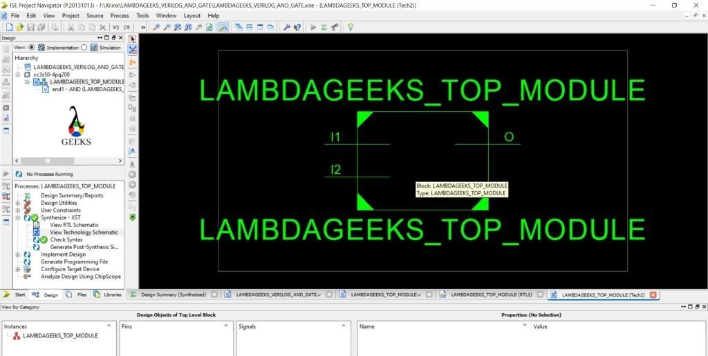
- Double Click inside the box of the diagram.
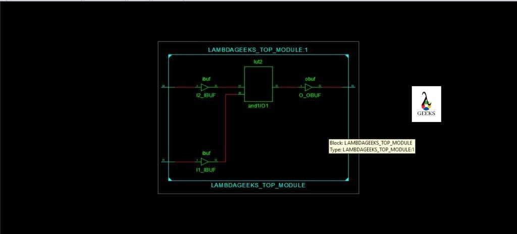
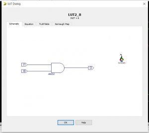
- A box will be there named – ‘lut2’. Double click on that.
It will display several diagrams.
The schematic Diagram:
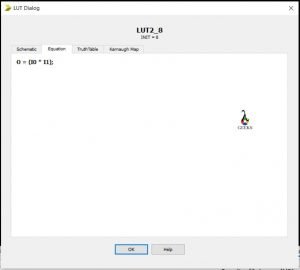
- Click on the Equation to see the relation.
- Click on the Truth table to find the truth table.
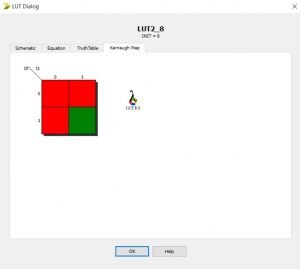
- Click on the Karnaugh Map to find the Map.
Check out our other VLSI articles!

Hi, I am Sudipta Roy. I have done B. Tech in Electronics. I am an electronics enthusiast and am currently devoted to the field of Electronics and Communications. I have a keen interest in exploring modern technologies such as AI & Machine Learning. My writings are devoted to providing accurate and updated data to all learners. Helping someone in gaining knowledge gives me immense pleasure.
Let’s connect through LinkedIn –