Microprocessor 8085:Registers & Important Addressing Modes

8085 Chip 300x108 1

Define Registers of Microprocessor 8085:

A register is a temporary  or short term storage space built into a CPU.”

More or less of the registers are applied internally but they cannot be accessed outside the processor.

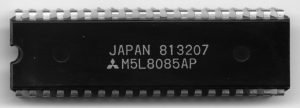
8085 Chip
Microprocessor 8085, Image Crdit – Myself User:ZyMOSIc-photo-Mitsubishi–M5L8085AP–(8085-CPU)CC BY-SA 4.0

What are the Types of the Register in Microprocessor 8085?

  • Accumulator (8 bit)
  • GPR (8 bit)
  • SP (16 bit)
  • PC (16 bit)
  • IR (8 bit)
  • TR (8 bit)
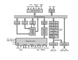
Http scanftree.com microprocessor Architechture Of 8085
Microprocessor 8085 Architecture , Image Credit – Vinay357Http—scanftree.com-microprocessor-Architechture-Of-8085CC BY-SA 4.0

Define Accumulator:

In the microprocessor 8085, accumulator specified as an 8 bit register connected with an ALU. This is utilized to hold one of the operand for arithmetical and logic-operation; it works as input to the ALU. The other operand for arithmetic and logical operation possibly stored either in memory or in GPR. But the final product will be stored in the accumulator only.
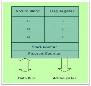
Register 8085
Register in Microprocessor 8085

Define General Purpose Register (GPR):

8085 microprocessor has 8 bit GPR; it works like a pair – B-C, D-E, H-L

The H-L register pair is used as a memory pointer & it holds 16 bit address of a memory location.

Define Stack Pointer (SP):

Stack pointer is a 16 bit especial purpose register. Stack is a order of memory location set by a programmer. The stack also perform as LIFO (Last in First Out). Here two operations are used; PUSH & POP.

Program Counter Definition:

A 16 bit register for specified operations ; comprises registers to load memory address from wherever the subsequent instruction is to be fetched.

Assume the program counter contains a memory location 7100H, this imply that microprocessor 8085 intended to fetch the instruction at the location 7100H.

Subsequently fetching the 7100H, the program counter is inevitably increses one count. This has the track of memory address of the instruction.

EXAMPLE: JMP, CALL, RETURN, RESTART etc.

Define Instruction Register:

This is an 8 bit register to hold the OPCODE of the instructions that has to be decode and execute. This is not accessible to the program writer.

Define Temporary Register:

This is a 8 bit non-programmable register utilized to keep data through an arithmetic and logical instruction implementation. TR is keeping intermediate results only and ultimate finalized end result is saved in the accumulator. This  is microprocessor dependendent, not  controlled by developer code.

Addressing Modes of Microprocessor 8085:

What is Addressing Mode?

“Addressing mode is the best way to define a certain data to be controlled by means of an instruction.”

Microprocessor has various kinds of addressing mode as it gives flexibility to the developer to get info and acessing data.

What are the types of Addressing Mode?

There are total five category as follows:

  • The Direct Mode
  • The Register Mode
  • The Immediate Mode
  • The Register Indirect Mode
  • The Implicit Indirect Mode

Direct Addressing Mode (DAM):

In this mode the address of the operand is identified the instruction the aforementioned. Instruction that includes direct address require 3-bytes of storage space of Microprocessor 8085.

  1. Instruction Code
  2. 16 Bit Address

Sample  instruction like STA 2500H stores the content of the accumulator in the memory location noted 2500H. Here 2500H is the address located in memory space where data is has be kept in.

Register Addressing Mode:

Here the operands are GPR. The opcode identifies the address of the register in addition to the operation to be executed.

For example  the instruction MOV A, B will move the data of register B to register A. In other instruction like ADD B, A; will first doaddition operation with the data of register B to register A and the end result is to be stored in register A.

Immediate Addressing Mode:

Here the operands are specified within the instruction itself, that means when any data has to be performed then immediately the operation is executed.

Example – MVI 05

                  ADI 05

Register indirect Addressing Mode:

In this case the operand will be identified by the register-pairs. Here accumulation is not linked directly.

Example are H-L, B-C, D-E etc.

Implicit Addressing Mode:

There are certain instructions which operates on the content of operator. These instructions will not call for address of operand.

Example – JMP, CALL, RAR

Timing Effects of Addressing Modes:

Addressing modes influence both the quantity of time necessary for executing an instruction and the total amount of memory necessary for storing. By way of instance, instructions which use suggested or register fixing, execute quickly because they deal directly with the chip hardware or with information present in hardware registers.

Most significant, however instruction can be fetched using one memory access. The Amount of memory accesses necessary is the factor in determining performance time, more memory accesses thus require more implementation time.

For example, to executing a CALL instruction requires 5 memory entrees;  out of these 3 will be for the access the entire instruction and the 2 will be for PUSHing the contents of the program counter onto the stack location.

The processor can access memory during every processing cycle. Each cycle includes a varying number of states. This is dependent upon the clk freq, and  which might vary from 480 nSec to 2µsec. The 8085 have clk freq around 5 MHz and so a minimal state may be of 200 nanosec.

What is Subroutine?

register

Creating a program of specific operation may happen several occasions and they’re not accessible as individual directions along with the application for such operation replicated over and over. However, the program ought to be written. The idea of subroutine is used to prevent the repetition of this smaller coding. The little program for specified for small job is called subroutine.

Subroutines are composed individually then saved to the primary memory by utilizing RET. CALL  instruction is generally utilized from the primary memory to subroutine.

Instruction Cycle of Microprocessor 8085:

This is the time taken by the microprocessor to finish the execution of the instruction. An instruction cycle usually consists of 1 to 6 machine cycles.

Machine Cycle

It is the time prerequisite to finish an operation through access one or the other the memory or I/O devices. It consists 3-6 T states. Here, opcode fetch, memory read, memory write, I/O read-write, operation executed. In the other word the operation of retrieving either memory devices or I/O devices is termed machine cycle.

T State:

This is the time equivalent to the one clock period in the basic unit used to calculate the time taken for the execution of the instruction and program in the microprocessor.

Fetch Operation:

The very initial byte of an instructionset is the OPCODE. An instruction usually more than 1 byte length. Another byte is for information data or  for the operand address. At the start of the cycle that the info of program counter where opcode can be obtained is forwarded to  the memory. This required  3 clock cycle another one is undefined.

What is the difference between CALL & JMP instructions of of Microprocessor 8085?

After a jump instruction is performed, the address given in JMP instruction is moved to PC. Thus application control is automatically progressed to this place location and carrying out as continued execution.

When CALL instruction is completed, microprocessor first keep PC info in the stack. Subsequently PC is occupied with the address set in the CALL instruction.Hence program control will transfer there.

What is Conditional & unconditional JUMP?

The JUMP commands are two kinds, specifically ‘unconditional jump’ and ‘conditional jump’.  If the microprocessor is indeed initiated to load a new address in the PC and commence instructions in that, it’s termed as an unconditional jump. In the instance of a conditional jump, the PC is loaded with a new address only when certain conditions are created from the microprocessor after reading the correct status of register bits.

For more Electronics related article click here
8085 Microprocessor: Interrupts,Functions & 7 Facts

2

Definition of Interrupt:

“Interrupt is the process of generating a momentary halt during program execution and permits peripheral devices to access the microprocessor”

8085 Architecture

Types of Interrupts:

Types of Interrupts according to delay:

  • Maskable
  • Non-maskable

Types of Interrupts according to grouping:

  • Vector
  • Non-vector

Types of Interrupts according to priority:

  • TRAP
  • RST 7.5
  • RST 6.5
  • RST 5.5

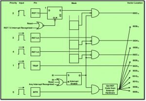
Block Diagram of 8085 Interrupts:

8085 Interrupt
8085 Interrupts

What is masking?

Masking can be implemented for the 4 hardware interrupts- RST 7.5, RST 6.5, RST 5.5 & INTR. In this figure, TRAP is NMI (Non Maskable Interrupt).

RST 7.5 alone has a F/F to recognise its edge transmission. The masking of interrupt can be done using SIM instruction. In additional a separate interrupt enables F/F is available to mask or allow the interrupts.

  • The maskable interrupts are masked by default by means of the reset signal.
  • The interrupt can be enabled by execution of EI instruction. So, to enable interrupts, after resulting the microprocessor the EI instruction must be used in 8085 microprocessor.
  • The 3 RST interrupts could be masked by load up the suitable word variety in the accumulation and implementing SIM instruction. This is known as software-masking.
  • All the maskable interrupts are disabled whenever an interrupt is recognized. So, it is essential to perform EI instruction every single time.
  • Altogether, the maskable interrupts may be disabled by performing DI instructions. The instruction resets an interrupt enable F/F in the microprocessor. For the enabling purpose, instruction EI is utilized.

TRAP:

  • It is non-maskable interrupt such that it need not to be enabled and cannot be enabled or disabled.
  • It is accessible to user
  • It is used for emergency situation such as power failure or energy shut off etc.
  • It is edged as well as level triggered that is the i/p should goes high and stay in this condition to acknowledgement.
  • TRAP has highest priority amongst all.

RST 7.5:

  • Its priority is just after the TRAP.
  • It is maskable such that both EI and DI operation can be possible.
  • It is sued for the situation whose priority is just after emergency situation.
  • It is positive edge triggered interrupt.
  • It can be triggered with a very short duration pulse.

RST 6.5:

  • Its priority is just after RST 7.5.
  • Other specifications are as same as RST 7.5.

RST 5.5:

  • Its priority is just after RST 6.5.
  • Other specifications are as same as RST 7.5.

INTR:

  • INTR is the lowest priority interrupt.
  • This is edge as well as level triggered.
  • Maskable and non-vectored type.
  • Both EI and DI can be possible in this situation.

Operation of INTR:

The signal flow sequence is as follows to INTR goes high.

  1. 8085 authorizations the status of the INTR, for carrying out an instruction.
  2. If INTR signal is 1, then 8085 will complete its present instruction and an active-low interrupt will be acknowledged by an interrupt ACK.
  3. Then the address of next instruction will be loaded in stack and will perform received instruction.

INTA:

  • It is not the interrupt just used by the microprocessor sent the acknowledgement. The process should be enabled by instruction.
  • During T3 condition of the opcode fetch, 8085 checks repeatedly of every instruction. If interrupt finds the microprocessor will complete execution instruction and ready for the restart sequence.
  • The restart sequence resets the interrupt F/F and active INTA upon receiving the signal.

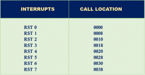
Interrupt Call Locations:

The call locations for 8085 are

TRAP- 0024

RST 7.5- 003C

RST 6.5- 0034

RST 5.5- 002C

SIM Operation (Set Interrupt Mask):

2

SIM (Set Interrupt Mask) for 8085 is explained as follows

M 5.5 – it is basically set to 1 to reset 5.5 mask

M 6.5 – it is also set to 1 to reset 6.5 mask

M 7.5 – it is also set to 1 to reset 7.5 mask

MSE – to mask interrupt

R 7.5 – it is reset RST 7.5 F/F

SDE – serial data enable set to 1 for sending

SOD – serial output data to be sent

EXPLANATION:

  • RST 7.5, 6.5 & 5.5 are maskable interrupts. The instruction EI and SIM utilized for enabling these.
  • BIT 0 to 2 is either set or reset the mask for RST 6.5, 7.5 & 5.5.
  • If a bit is set to 1, then the interrupt is masked off i.e., disable. If set as 0, the respective interrupt is enabled.
  • If bit 3 is set to 1 to mask on bit 0 to 2.
  • BIT 4 is additional control for RST 7.5. If it is set to 1 the RST 7.5 is reset.
  • Bit 6 and 7 are serial output data where bit 6 is to enable SOD and bit 7 may be either high or low. The instruction DI disable all the interrupts.

PENDING REQUEST:

When 1 interrupt request is being served, other interrupts may occur resulting in pending request. When more than 1 interrupt occur simultaneously then interrupt having higher priority has served and interrupt having lower priority remain in the pending condition.

8085 microprocessor has an additional instruction called RIM (Read Interrupt Mask) to sense the pending interrupt.

RIM Operation (Reset Interrupt Mask):

3

RIM (Read Interrupt Mask) for 8085 is explained as follows

M 5.5:  This bit is set to 1 if RST 5.5 is masked. The bit 0 to 2 could be used for interrupt mask utilizing RIM instruction

M 6.5: This bit is set to 1 if RST 6.5 is masked.

M 7.5: This bit is set to 1 if RST 7.5 is masked.

IE:  It is set to 1 if all interrupts are enabled.

I 5.5: It is set to 1 when RST 5.5 is in pending condition.

I 6.5: It is set to 1 when RST 6.5 is in pending condition.

I 7.5:  It is set to 1 when RST 7.5 is in pending condition.

SID:  Serial Input Data; it will be either 1 or 0 for input purpose.

Vectored Interrupts:

TRAP, RST 7.5, RST 6.5, RST 5.5 (call location).

4
5
6

SOFTWARE INTERRUPTS VS HARDWARE INTERRUPT:

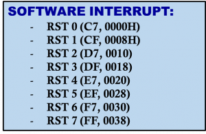
         Software Interrupts    

This are the software instructions when they are executed, CPU branches to ISR.

These are slower than the hardware interrupts.

 
Examples – RST 0, RST 1, RST 2 etc.
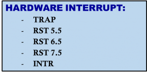
        Hardware Interrupts    

These are physical input from external devices which causes CPU to branch to ISR.

  These are faster than software interrupts.  


Examples – TRAP, RST 7.5 etc.

What is Stack?

Stack

A stack in 8085 microprocessor is a set of memory location in read-write memory specified by a programmer in a main program. These memory locations are utilized to store binary data momentarily during coding.

The initiation of the stack is defined in the program by executing the basic load instruction such as LXI SP. This generally load a sixteen bit memory address in the SP register.

Types of Stack:

  1. PUSH
  2. POP

PUSH – In the course of execution, PUSH is required to resolve the problem of certain register since the registers are prerequisite for some additional execution in consequent state. These contents move to certain memory location by a special function register is called PUSH.

Example-

                LXI SP, 2099 H

               LXI H, 42F2 H      

               PUSH H

  1. Loads the contents of 2099H with SP register that is reserved in read-write memory as a state and the location begins from 2098H in moving upward for temporary storage.
  2. LXI H, 42F2H describes the loading of H-L pair i.e., (42) is loaded in H and F2 is loaded in L.
  3. PUSH H indicates that the content of H i.e., 42 stored in 2098H and the content of L i.e., F2 is stored in 2097 H.

POP – After completion of this operation this content which are saved in the temporary register are transferred back to the main memory by the operation of POP.

 Example –

                          LXI SP, 2099 H

                          LXI H, 42F2 H

                          PUSH H

                          DELAY COUNTER

                          POP H

The contents of register H-L pair are not destroyed. It is available of the delay counter in the content of the program counter. The content of the top stack location shown by SP appear into the register L and SP will increase 1.

The content of top of stack i.e., 2097 is shifted to 2098 and 2099 by 1 incarnated and from the temporary register the contents move to the main register.

For more about 8085 microprocessor click here

Encoder & Decoder Circuit:Definition,Working,5 Applications

8 3 Encoder 300x141 1

Encoder Definition

An encoder is a digital combinational circuit that converts binary information of maximum 2n input lines into n output lines. The correspondent input binary value generates the output lines.

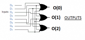
Encoder Circuit

8 3 Encoder
Encoder Circuit, Image Source –Nitianabhigyan8-3 EncoderCC BY-SA 4.0

Example of an encoder:

Octal to Binary Encoder

It has inputs for each of the octal digits that is a total of eight in number. It has three output lines (according to the rule that the 2n input line encoder will have n output line). The outputs represent the numbers in binary.

The encoder can be implemented using OR gates. Output C is equal to 1 if the octal digit’s value is 1, 3, 5, 7. The output B will be one if the octal number has a value of 2, 3, 6, 7. The output AS will be one if the input octal digits’ value is 4, 5, 6, 7. The following Boolean expressions represent the outputs.

A = O4 + O5 + O6 + O7

B = O2 + O3 + O4 + O7

C = O1 + O3 + O6 + O7

O0O1O2O3O4O5O6O7ABC
10000000000
01000000001
00100000010
00010000011
00001000100
00000100101
00000010110
00000001111
Octal to Binary Encoder Truth Table

The encoder implemented at the table has the only limitation. That is, only one input can be in active mode at any given time. That is why if two inputs are made active, then the output lines produce undefined outputs.

Let us take an example if the input O3 is in an active state as well as input O6 is also in an active state, then the encoder produces output as 111. The result neither represent O6 nor O3. So, there is a mess.

To solve this problem, new encoders are designed with an input priority to make sure that only one input gets enabled at a time. If priority is set high for higher digits in this new system, then for enabled O3 and O6, the output will be 110, representing 6 in binary. This happens as O6 has a higher priority than O3.

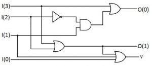
Priority Encoder

 A priority encoder is a particular type of encoder circuit which has a priority function for the inputs. The priority function works in the real world. For example, if there is a queue and you have a high priority, you go first! If there is an operation where both the input values are 1, then the 1 with the highest priority will take precedence.

O0O1O2O3ABY
0000XX0
1000001
X100011
XX10101
XXX1111
Truth Table for Priority Encoder

As we can see from the truth table of the priority encoder, it has three outputs. Two are general outputs; another one, Y, is a valid bit indicator.

The right bit indicator is set to 1 when one or more than one input has a value of 1. If there are such conditions, where all inputs are set to 0 or the information is not valid, then Y also becomes 0. There is no checking of other outputs if the Y term is 0.

Then, they are specified as don’t-care terms. Truth tables use don’t-care words to represent 0 or 1 rather than listing up 16 terms for variables. For example, 100X means either 1000 or 1001.

As mentioned earlier, the higher the subscript number, the priority of the number gets high. From the truth table, we can see that input O3 has the highest priority as the input. That is why whatever the values for other input digits when the O3 value is 1, the output becomes 11. Similarly, O2 has a priority lower than O3 and higher than O1 and O0. When the input of O2 is 1, the result will be 10. In the same way, for O1, the output is 01, and for O0, the outcome will be 00.

The Boolean function for the priority encoder will be:

A = D2 + D3

B = D3 + D1 D2’

Y = D0 + D1 + D2 + D3

priority
Priority Encoder Circuit, Image Source – NitianabhigyanA 4-2 Priority Encoder CC BY-SA 4.0

How does a priority encoder circuit differ from multiplexer? Read Here!

DECODERS

Definition and Overview

A decoder is a combinational circuit that does the opposite operation of an encoder circuit. It decodes or simplifies the encoded information from n input lines to a maximum of 2n output lines.

Decoder Circuit

Decoder
Decoder Circuit and Truth Table, Image Source –BlueJester0101Decoder ExampleCC BY-SA 3.0

Binary codes represent information of distinct quantities. An n bit binary code can represent a maximum of 2n different elements of encoded data. A decoder decodes that information and provides the output.

Decoders are specified as numbers of input to numbers of output line decoders. If the number of input lines is n, then there will be a maximum of 2n output. Every single input combination produces a distinct output value.

To illustrate the working of a decoder, let us take the example of a 3:8 decoder. The specification suggests that the circuit will decode the three input lines into eight outputs of every single output represents the min-terms. The connected NOT gates inverts the input data lines whenever necessary. The AND gates (total eight in number) produces the min-terms (each for one output).

ABCO0O1O2O3O4O5O6O7
00010000000
00101000000
01000100000
01100010000
10000001000
10100000100
11000000010
11100000001
Decoder Truth table

From the truth table, we can observe that seven outputs have a value of 0 and one output, which have a value of 1. The outcome, which has a value of 1, represents the actual input value or the min-term.

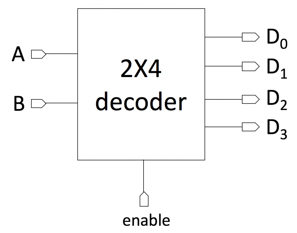
There are decoders that are constructed with universal basic gates like NAND and NOR. Using a NAND gate is economical as well as efficient to build a decoder.  Decoders also need to enable inputs like encoders. The decoder gets enabled when the enable input pin has a value of 0. Only one output may have a value of 0 at a time, and the rest of the outputs will be equal to 1. The truth table below simplifies the operation.

EnableABO0O1O2O3
1XX1111
0000111
0011011
0101101
0111111

The circuits get disabled if the E value is set to 1. Like the encoder circuit, if the E value is set to 1, there will be no checking of other inputs. In the disabled state of the decoder, no outputs have the value 0, and no min-term is elected. Many decoders have more than one enables pin. They need to abide by the logical operations to perform as a decoder.

A demultiplexer can be made using a decoder if the decoder is added with enable inputs. Parallelly corresponding decoders can make large decoders.

Implementation of logic using decoders

A decoder has 2n input data lines and n output lines. 2n represents the minterms, and n represents the number of variables using which the minterms are formed. As mentioned earlier, for each combination of inputs, there are different outputs.

A decoder can be used to implement logic gates as Boolean functions are nothing but the sum of minterms. An OR gate connected with a decoder can implement the logic of a Boolean function.

Decoder
Decoder with an enable

Applications of Encoders and Decoders

Encoder circuit and decoder circuit have applications in smart digital devices as they are significant for today’s’ digital era.

Some of the significant applications are –

  1. Speed Control of modern motors.
  2. Night vision cameras
  3. Metal detectors
  4. encoder circuit has applications in Robotic vehicles
  5. Automation system – especially the home automation system.
  6. Automatic Monitoring systems has different types of encoder circuits.
  7. Encoder circuit has utilized in encrypted communications system.

7 Facts On Multiplexer And Demultiplexer: Beginner’s Guide !

  • Definition & Overview of Multiplexer
  • Operation & Analysis
  • Implementation of Boolean Function using MUX
  • DEMUX
  • Application of MUX-DEMUX

Definition:

A digital multiplexer is a device that takes more than one inputs and outputs a single selected data. Just like an adder and subtractor, a multiplexer is also a combinational device.

It is also identified as a data selector as it pick out one of several inputs and sends it to the output with the help of a control signal or select lines. If a typical MUX has 2n input lines, then there will be n choose lines. The bit combination of select lines determines which output will be produced.

2:1 MUX Definition:

A 2:1 MUX signify that the multiplexer has two input and one output. It also has one select line as S. If S =0, the upper AND gate are ON, and I0 appears at the o/p, and if the S =1, the lower AND gate is ON and I1 appears at the o/p. MUX acts like a switch which chooses one out of two available input.

Multiplexer 2 to 1
A 2:1 Multiplexer with the Boolean equation, Image source – en:User:CburnettMultiplexer 2-to-1CC BY-SA 3.0

4:1 MUX Definition:

A 4:1 MUX means that the multiplexer has four input lines and one output line. It has two select lines as S0 and S1. There are several AND gates to produce the output. Select lines are connected with the correspondent AND gates. The result of AND gates are connected to a single OR gate.

If the select lines give the binary code as 10, that is, S1 = 1 and S0 = 0, then the AND gate connected with input I2 has two of its inputs equal to value 1, and the last one is connected with I2. The other three AND gates have at least one input equal to zero, this correspondingly changes their output equal to zero. Here and now, the outcome of the OR gate is analogous to the value of I2 and allows the designated input to look as if at the result. 

Multiplexer 4 to 1
A 4:1 Multiplexer block diagram, Image by – en:User:CburnettMultiplexer 4-to-1CC BY-SA 3.0

Operation & Analysis

A multiplexer is very much similar to a decoder. The AND gates and the NOT gates bring the similarity between a decoder and multiplexer. Meanwhile, a MUX truly decodes the select lines and provides the output. A multiplexer can also be constructed from a decoder. If 2n input lines – each to AND gate are added up with an n to 2n decoder, the circuit will work as a multiplexer.

The multiplexer size depends on the data input lines that are 2n and the single output line. The number of selection lines will be n for a 2n input line mux. Like a decoder, a mux may also have an enable input line. The outputs will be disabled if the enable input is in an inactive state. When the enable pin is in an active state, the MUX will work as usual.

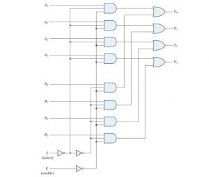
There are efficient techniques to be responsible for multiple bit selection-logic. If the multiplexer circuits are combined with standard selection inputs, the numerous bit selection can be implemented. To implement this, a quadruple 2:1 mux is shown in the below image.

MUX
Quadruple MUX

Here, the circuit has four multiplexers, and they are 2:1 mux. The output Y0 can be selected from input A0 or B0. Similarly, the output of Y1 can be selected from input A1 or B1, and it continues for the rest of the circuit. The select lines S selects one of the lines for each of the multiplexers. The enable input must be in an active state to operate the multiplexers.

Though the circuit has a 2:1 multiplexer for operation, it looked like a circuit that pick out anyone of the two 4 -bit sets of data line. Now, when the enable is 0, and the select line is also 0, the four an inputs can appear as the output. Also, if the s=1, then the B inputs appear at the result. The outcomes will be 0 when the enable pin is set to 0, no matter the value of select lines.

Implementation of Boolean Function using MUX

Boolean functions can also be implemented using multiplexers. The min-terms of a function can be generated in a multiplexer with the circuit connected with the selection lines. The data inputs can select separate min-terms. This is how implementations of n variable function are possible for a multiplexer of input data lines of 2n and n select lines. The input data lines will be used for each min-term.

A more efficient way to implement Boolean expression is also available. A function of n variables can be implemented with a multiplexer having n-1 lines. The first n-1 variable is utilized as selection inputs. The remaining variable of the operation is used for data inputs. If each data input denotes the remaining variable, the mux will be a, a’, 1, or 0.

We can take the example of a Boolean algebra.

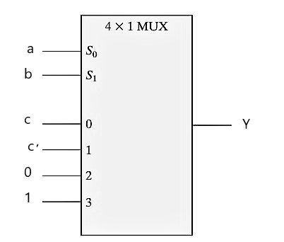
F (a, b, c) = ∑ (1, 2, 3, 4)

The function of three variables can be implemented with a 4:1 MUX, as shown below.

BOOLEAN MUX
Implementation of Boolean Functions

The two variables, a and b, are applied to the select lines in a certain order. The a  is connected to the S1 input, and b is linked with the S0 input. The truth table of the function determines the values for the input lines of the MUX. When ab = 00, output F is equal to c as F = 0 when c = 0 and F = 1 when c = 1. Data input 0 requires the input for variable c.

The multiplexer works in a certain way. When the value of ab is zero, then the data input 0 appears at the output. Thus, the output becomes equal to c. The data lines 1, 2, 3 also required inputs and can be determined similarly. The inputs are derived from the function F, and the inputs are ab = 01, 10, 11.We can find out the inputs for the data lines by this explanation.

This example shows the typical steps to implement Boolean functions consisting of n variables with the help of a multiplexer with n – 1 selectionline and 2n-1 dataline. The truth table of the Boolean function is described initially. The primary n-1 variables of the process given are applied to the selection input of the MUX. The output is calculated as the last variable’s function for every single combination of the selection lines. The process has a specific set of values. The function’s value can be 0 or 1, or the variables or the complement of the variables.

Now let us take an example of a more considerable Boolean function.

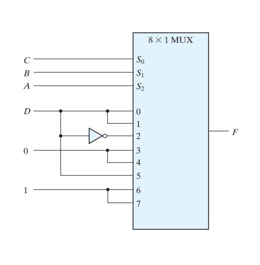
F (A, B, C, D) = ∑ (1, 3, 5, 7, 9, 11, 13, 15)

A multiplexer can implement this Boolean function with three select lines and eight input lines (Basically an 8:1 MUX). The MUX is shown in the image.

BOOLean MUx 2
8 x 1 MUX

Now, the first variable that is A, should be connected to the select line S2 to make sure the correspondent select lines for B and C becomes S1 and S0. The truth table of the function is depicted as mentioned earlier. The values for the input lines for the MUX is calculated from that truth table. The data line number is determined by the binary combinations of the variable ABC.

If ABC = 101, then F comes as D. Form this, it can be calculated that data input line 5 receives input as D. Logic 0 and logic 1 are two fixed values. Logic 0 means logic low or equivalent to ground, and logic 1 means logic high or the input power signal.

Three State Gates

The construction of a multiplexor is possible using three-state gates. Three state gates are the digital circuitries that can operate in three states. Two out of those three states are 0 and 1 conventionally, and the third state is known as the high impedance state. At the high impedance state, the logical procedure performs like an open circuitry. Three state gates can perform all types of logical operations, such as NOT or NOR. The most common use of a three-state gate is as a buffer gate.

As said earlier, multiplexers can be constructed using three-state buffers. The image below describes the implementation of a 2:1 mux with two three-state buffer and a NOT gate. The two outputs are connected for providing a single result. When the select line is valued as zero, the upper pad gets activated, and the lower one gets disabled. A appears at the output, and when the select input is 1, the reverse happens, and B appears at the result.

DEMUX

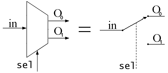
A DEMUX or de-multiplexer is a digital device that does the opposite of a multiplexer. It takes a single input and provides multiple outputs with the help of select lines. If a DEMUX has n select lines, then the numbers of production will be 2n. A diagram of 4:1 DEMUX is given below.

A Demultiplexer , Image Credit – FresheneeszDemultiplexerCC BY-SA 3.0

MUX & DEMUX Applications:

MUX and DEMUX have importance in today’s digital era. Some of their applications are –

Mux-Demux,Image – Tony R. Kuphaldt, Telephony multiplexer systemCC BY 1.0
  • Communication System: MUX and DEMUX have the most extensive applications in the field of communication systems. MUX allows transmitting distinct types of data like – audios and video, images, voice recordings, etc. can be multiplexed into a single transmission channel. It increases the efficiency of the system.
  • Telephonic System: Telephone networks need both MUX and DEMUX. Technologies like – Frequency Division Multiplexing (FDM), Time Division Multiplexing (TDM), Code Division Multiple Access (CDMA), etc., are possible only because of MUX and DEMUXs.
  • MUX and DEMUXs are also used in logic gates for combinational circuits and many other digital devices.

7 Facts On Binary Subtractor: Half & Full Subtractor

Half subtractor using NAND 300x155 1
  • Definition and Overview of Binary Subtractor
  • Half Subtractor
  • Full Subtractor
  • N -bit Subtractor
  • Applications of binary subtractor
  • VHDL implementation of half subtractor and full subtractor

Definition

A subtractor is a device that subtracts two numbers and produces the result. A digital or binary subtractor is something that deals with the Subtraction of binary digits.

A binary subtractor is needed for digital computation inside a digital device or a digital computer. The most convenient way of Subtraction unsigned binary numbers is the method of complements. There are rules for binary Subtraction.

The binary subtraction rules are stated as follows. Here 0 is logic low, and one is logic high. A and B are two inputs.

ABY = A – B
000
011 (borrow 1)
101
110
Binary Subtraction truth table

Example of subtraction operations:

1101 – 1011

1101

– 1011

= 0010

So, the answer is 0010

Methods of complements can alternatively carry out binary subtractions for binary subtractors. There are two types of complement methods that are generally used.

A.  1’s Complement

B. 2’s Complement

Steps for performing 1’s complement:

  1. Find out the 1’s complement of the number that is to be subtracted.
  2. Now the 1’s complement is added to the number from which the Subtraction is desired.
  3. Where there is one carry in the last position, of the result of the addition in step 2, the carrier is removed and added to the product without the carry to obtain the final result.

Let us take an example – 1101 – 1011

1’s complement of 1011 = 0100

Now, add 1101 with 0100

1101

 + 0100

 = 1 0001

As we can see, there is one as a carry, so we remove the carry and add the carry again with the obtained result.

0001

+    1

= 0010

So, the answer to the Subtraction is 0010

For 2’s complement method

  1. Calculate the 2’s complement.
  2. The complement is now added with another number.
  3. The carry is rejected.

Let us take an example – 1101 – 1011

2’s complement of any number is calculated by performing 1’s complement and adding 1 to it.

2’s complement of

Now, add 1101 with 0100

1101 + 0100 = 1 0001

As we can see, there is one as a carry, so we remove the carry and add the carry again with the obtained result.

0001 + 1 = 0010

So, the answer to the Subtraction is 0010

Digital computers use the 2’s complement method for calculations as it requires less carry.

The complement methods in the decimal number system are known as 9’s and 10’s complement method.

Various digital circuitries implement this subtraction operation. They are –

  • Half Subtractor
  • Full Subtractor

A binary subtractor not only performs addition operations but also used in digital applications. Decoding and encoding of values, calculation of the index is a few of its applications.

Half subtractor

A half binary subtractor is a binary subtractor that subtracts one bit of data and produces the result. It has two input sides through which we supply the digital logic values, and it has two outputs through which we receive the impact of the operation. The result can be shown in a single digit. The work shows the number in the Subtraction that has the same significance as the individual digits subtracted. The other output shows the borrow bit.

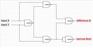
Half subtractor using NAND
NAND gate implementation. Image Credit – NitianabhigyanHalf subtractor using NANDCC BY-SA 4.0

The half subtractor truth table

The working of the half binary subtractor is shown in the following truth table.

ABDifferenceBorrow
0000
0111
1010
1100
Truth table for half binary subtractor

Half Subtractor circuit

From the truth table, we can conclude that the first three rows can represent the result using a single digit. In the second row, the work is described using two numbers as it has borrowed as 1.

Difference = A′B + AB′

Borrow = A′B 

So,

Difference = A XOR B

Borrow = A′ AND B

We need one XOR gate, one NOT gate, and one AND gate to implement the logic. XOR gate, NOT gate, an AND gate can also be made using universal gates like NAND and NOR. So, a half subtractor can be designed using only universal gates.

The following image shows A and B as the input and D as the difference, and C as they borrow.

Half  Binary Subtractor
Half Subtractor

Full Subtractor

Full Binary Subtractor is another kind of binary Subtractor which provides the result of a binary subtraction operation. When two binary numbers are subtracted, except for the least significant digit, there is a borrow-in as Bi-1 and borrow out as Bi. The full Subtractor is designed to handle a borrow-in for each stage. That is how an entire order overcomes the shortcoming of half Subtractor of running borrow-in.

A full subtractor truth table

XiYiBi-1DiBi
00000
00111
01011
01101
10010
10100
11000
11111
Full Subtractor truth table

Full subtractor circuit

Difference = A′ B′ Bin + A B′ Bin′ + A′ B Bin′ + A B Bin 

Borrow = A′ Bin + A′ B + B Bin 

To implement the expression using logical gates, we need to simplify the word further.

Difference = A′ B′ Bin + A B′ Bin′ + A′ B Bin′ + A B Bin 

 Or, Difference = Bin (A′B′ + AB) + Bin ′ (AB′ + A′B)

 Or, Difference = Bin (A XNOR B) + Bin ′ (A XOR B)

 Or, Difference = Bin (A XOR B) ′ + Bin ′ (A XOR B)

 Or, Difference = Bin XOR (A XOR B)

  Or, Difference = (A XOR B) XOR Bin

Borrow = A′ B′ Bin + A B′ Bin′ + A′ B Bin′ + A B Bin 

 Or, Borrow = A′ B′ Bin +A′ B Bin ′ + A′ B Bin + A′ B Bin + A′ B Bin + A B Bin

 Or, Borrow = A′ Bin (B + B′) + A′B (Bin + Bin ′) + B Bin (A + A′)

 Or, Borrow = A′ Bin + A′B + B Bin

The expression can be written in another way –

Bout = A′ B′ Bin + A′ B Bin′ + A′ B Bin + A B Bin     

    Or, Borrow = Bin (AB + A′ B′) + A′ B (Bin + Bin′)

     Or, Borrow = Bin (A XNOR B) + A′ B

    Or, Borrow = Bin (A XOR B) ′ + A′ B

Full Binary Subtractors
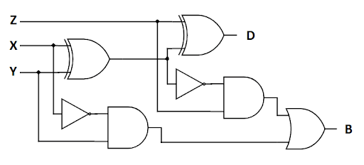
Full Subtractors , X,Y, Z are input

As the circuit diagram shows, A, B, and Bin. The circuit gives two output as difference output and borrows output. The Bin is set to 1 whenever there is borrow in input A. Bin is then subtracted from A and Y.

The general expression can be written as D = A – B – Bin + 2 Bout.

Full subtractors can also be implemented using half subtractors.

1920px Full sub Fixed.svg
Full Subtractors using Half Subtractor

N bit Subtractor

In a single bit binary subtractor, Subtraction of only 1 bit can be performed. If we need to perform Subtraction of n -bit, then a n bit binary subtractor is required. An n-bit subtractor can be implemented similarly using subtractors in a cascaded form.

Applications of Subtractors

  • Subtractors are often used with adders. Whenever an adder is needed for a circuit, a subtractor is also required.
  • ALU, which is responsible for the calculation, and stays inside a microprocessor, also needs subtractors. CPUs also need subtractors for operation.
  • Microcontrollers also use subtractors for performing the digital computation.
  • Subtractors are also used in Digital Signal Processing Domain.
  • Digital computers use a lot of subtractors.

VHDL Implementation of Half Subtractors & Full Subtractors

Half Subtractor Data flow Modelling

library IEEE;

use IEEE.STD_LOGIC_1164.ALL;

entity ENTITY_NAME is

    Port ( A : in  STD_LOGIC;

           B : in  STD_LOGIC;

           IB : in  STD_LOGIC;

           Diff : out  STD_LOGIC;

           Borr : out  STD_LOGIC);

end ENTITY_NAME;

Architecture Dataflow

architecture Dataflow of ENTITY_NAME is

begin

Diff <= (A xor B) xor IB;

Borr <= ((not A) and (B or IB)) or (B and IB);

end dataflow;

Full Subtractor Dataflow Modelling

entity ENTITY_NAME  is

    Port ( A : in  STD_LOGIC;

           B : in  STD_LOGIC;

           IB : in  STD_LOGIC;

           Borr : out  STD_LOGIC;

           Diff : out  STD_LOGIC);

end ENTITY_NAME;

Architecture dataflow

architecture Behavioral of ENTITY_NAME is

begin

process(A,B,IB)

begin

if(A=’0′ and B=’0′ and IB=’0′ )then

Diff<=’0′;

Borr<=’0′;

elsif(A=’0′ and B=’0′ and IB=’1′ )then

Borr<=’1′;

Diff<=’1′;

elsif(A=’0′ and B=’1′ and IB=’0′ )then

Borr<=’1′;

Diff<=’1′;

elsif(A=’0′ and B=’1′ and IB=’1′ )then

Borr<=’0′;

Diff<=’1′;

elsif(A=’1′ and B=’0′ and IB=’0′ )then

Borr<=’1′;

Diff<=’0′;

elsif(A=’1′ and B=’0′ and IB=’1′ )then

Borr<=’0′;

Diff<=’0′;

elsif(A=’1′ and B=’1′ and IB=’0′ )then

Borr<=’0′;

Diff<=’0′;

else

Borr<=’1′;

Diff<=’1′;

end if;

end process;

end Behavioral;

7 Facts On Facts On Binary Adder:Full Adder & Half Adder

Half Adder 300x167 1
  1. Definitions and Overview of adder
  2. Types of adder
  3. Half adder
  4. Full adder
  5. BCD adder

Definitions:

An adder is a device which add up two numbers and produce the result. A binary adder is something which deals with addition of binary numbers.

A binary adder is a digital device and needed for digital computations. The operation performed in a binary adder, obeys the rules of binary addition. Here two bits corresponding to 2n are added and the resultant is then added to the carry from the 2n-1 digit.

The binary addition rules are stated as follow. Here 0 is logic low and 1 is logic high. A and B are two inputs.

ABY = A + B
000
011
101
110 (carry 1)
Binary Addition

Example of addition operations:

  • 11111 + 1011 + 101 + 10 + 1
  • 11111+ 1011 = 101010
  • 101010 + 101 = 101111
  • 110001 + 1 = 110010

So the answer is 110010

Types of Adder

This addition operation is implemented by various digital circuitries. They are –

  • Half Adder
  • Full Adder
  • BCD Adder

A binary adder not only performs addition operations but also used in other digital applications. Decoding of address, calculation of index are few of its applications.

Half Adder

A half adder is a type of binary adder which add one bit of data and produces the result. It has two input side through which we supply the digital logic values and it has two outputs through which we receive the result of the operation. The result can be shown in a single digit. The output shows the digit in the sum that has the same significance as the individual digits added. The other output shows the carry bit.

Half Adder Truth table

The operation of the half adder is shown in the following truth table.

ABSumCarrySum of A & B
000000
011001
101001
110110
Truth Table of Half Adder

Now from the truth table, we can observe that the first three rows can represent the sum using a single digit. At the last row, the sum is represented using two digits as it has 1 as carry. Here the sum is zero and carry 1 must be taken to the position of next higher significance.

Sum = A′ B + A B′

Carry = AB

So,

Sum = A XOR B

Carry = A AND B

To implement the logic, we need one XOR gate and one AND gate. XOR gate and AND gate can also be made using universal gates like NAND and NOR. So, a half adder can be designed using only universal gates.

The following image shows A and B as the input and S as the sum and C as the carry.

Full Binary Adder
Half binary adder , Image Source – inductiveloadHalf Adder, marked as public domain, more details on Wikimedia Commonsmedia

Full Adder

Another type of binary adder is full adder. It also adds binary data and produces the output. Now, when two binary numbers are added, except the least significant digit there is a carry-in as Ci-1 and carry-out as Ci. The full adder is designed to handle a carry-in for each stage. That is how a full order overcomes the shortcoming of half adder of handling carry-in.

Full adder truth table

AiBiCi-1SiCi
00000
00110
01010
01101
10010
10101
11001
11111
Full Adder Truth Table

Full Adder Circuit

Si = Ai Bi Ci-1 + Ai Bi Ci-1 + Ai Bi Ci-1 + Ai Bi Ci-1 + (Ai Bi + Ai Bi) Ci-1   + (Ai Bi + Ai Bi) Ci-1

And the carry comes as:

Ci = Ai Bi Ci-1 + Ai Bi Ci-1 + Ai Bi Ci-1 + Ai Bi Ci-1 

Or, Ci = (Ai Bi + Ai Bi) Ci-1   + (Ai Bi + Ai Bi) Ci-1

Or, Ci = Ai Bi + (Ai Bi + Ai Bi) Ci-1

Now, consider a half adder has inputs A and B. The output sum is S and carry is C. Now the expression of Si and Ci can be obtained from the expressions of Sum and carry of half adder circuit.

Si = S Ci-1 + S Ci-1

Ci = C + S Ci-1

Now, to implement a full adder using half adders we need two half adders and one OR gate. Full adder implementations using half adders is represented in the below figure.

Full adder logic diagram
Full binary adder , Image Source – InductiveloadFull-adder logic diagram, marked as public domain, more details on Wikimedia Commons

As we can see in the figure that the first half adder (marked as-) has the input Ai and Bi. The second half adder (marked as-) has inputs of C i-1 and output of the first half adder that is S. The output of the second half adder are Si and S Ci-1.

Now, S Ci-1 represents the carry out. The carry of the first half adder that is C and the carry of the second half adder that is S Ci-1 are fed as input of a OR gate. The output of the OR gate is the final carry out of the full adder circuit.

Parallel Binary Adders

A full adder is needed for the addition of bits in each stage of addition except the addition of least significant digits on the other hand two half adders are needed to complete a full adder. It follows the rule that the addition of two n-bit numbers will require 2 * m -1 number of half adder and m-1 numbers of OR gates. This type of binary adders is known as parallel binary adders. The speed of operation of these types of adders are very fast. That is why they are preferred in modern computational devices.  

Let us add 101 and 111 as an example of parallel binary adder. The figure shown below represents the addition.

4 bit carry lookahead adder
Parallel binary adder, Image source – en:User:Cburnett4-bit carry lookahead adderCC BY-SA 3.0

The first half adder (marked as-1) adds the extreme right-hand bits 1 and 1 to produce the binary sum 0 and the carry 1 according to the rules of binary addition. The output of the half adder is fed into the input of the first full adder (marked as- 2). The other two inputs of first full adder are the two next bits that is 0 and 1. The outputs of the first full adder are 0 as sum and 1 as carry. They are further fed into input of second full adder. The other two inputs are 1 and 1. The outputs of the second full adder is 1 as sum and 1 as carry. So, the result of the summation is 1100.

Now, a point to be noted that in place of a half adder at the least significant digit position, a full adder can be used with its carry input made 0.

BCD Adder

The term BCD in BCD adder stand for Binary Coded Decimal. BCD is a special type of binary encoding where each digit has certain number of bits for representation. The BCD of first 10 decimal value is shown in the table.

Decimal Digit BCD  
00000
10001
20010
30011
40100
50101
60110
70111
81000
91001
BCD ADDER

BCD adder has two inputs which varies from 0 to 9. The output varies from 0 to 18 and if the previous carry is considered then the range will be up to 19.

The table for BCD adder is given below.

decimal or bcd adder
BCD Adder Truth Table

From the above table, we can observe that from 1 to 9 the binary and the BCD is same. From 10 to 19 decimal numbers, both the binary and codes are different.

The circuit diagram of a BCD adder is shown below.

  • In the above diagram there is a four-bit binary adder which has input as addended and augend. It has also input of carry.
  • The binary adder gives output of the addition and an carry output.
  • Now, using the output and the carry the circuit is further designed to find out the final carry.
  • The output is further fed into a 4-bit adder.
  • Now, the circuit is designed to make the 1st and 4th bit of the addended number as 0 and also the 2nd and 3rd bit to make as same as Carry. When the carry is 1, the circuit is designed in such a way that the addended will be 0110. 6 is added with augend to get the BCD.

Example of BCD

0110 + 0101 = 1011

Now this is invalid as BCD. The number is greater than 9. So, we have to add 6 to the result.

The final result will be = 1011 + 0110 =

1011 + 0110 = 10001

So the final answer will be 10001

Know about Subtractors! Click Here!

VHDL implementation of Half adder and Full Adder

HALF-BINARY ADDER DATAFLOW MODELLING

library IEEE ;

use IEEE.std_logic_1164.all ;

entity half_adder_dataflow is

    Port ( a : in  STD_LOGIC;

           b : in  STD_LOGIC;

           s : out  STD_LOGIC;

           c : out  STD_LOGIC);

end half_adder_dataflow;

architecture Behavioral of half_adder_dataflow is

begin

s <= a XOR b;             

c <= a AND b;            

end Behavioral;

HALF- BINARY ADDER BEHAVIORAL MODELLING:

entity SUDIPTA_ROY_HALFADD is

    Port ( A : in  STD_LOGIC;

           B : in  STD_LOGIC;

           C : out  STD_LOGIC;

           S : out  STD_LOGIC;

           Z : out  STD_LOGIC);

end SUDIPTA_ROY_HALFADD;

architecture Behavioral of SUDIPTA_ROY_HALFADD is

begin

process(A, B)

begin

if(A=’0′ and B=’0′) then

S <=’0′;

C <=’0′;

elsif(A=’0′ and B=’1′) then

S <=’1′;

C<=’0′;

elsif(A=’1′ and B=’0′) then

S <=’0′;

C<=’1′;

else

S <=’1′;

C<=’1′;

end if;

end process;

end Behavioral;

FULL-ADDER DATAFLOW MODELLING

library IEEE;

use IEEE.STD_LOGIC_1164.ALL;

entity SUDIPTA_ROY_FULLADD is

    Port ( A : in  STD_LOGIC;

           B : in  STD_LOGIC;

           Cin : in  STD_LOGIC;

           S : out  STD_LOGIC;

           Car : out  STD_LOGIC);

end SUDIPTA_ROY_FULLADD;

architecture Dataflow of SUDIPTA_ROY_FULLADD is

begin

S<=(A xor B) xor Cin;

Car<=( A and B) or (B and Cin) or (Cin and A);

end Dataflow;

FULL-ADDER BEHAVIORAL MODELLING

entity SAERI_DATT_FULLADD is

    Port ( A : in  STD_LOGIC;

           B : in  STD_LOGIC;

           Cin : in  STD_LOGIC;

           S : out  STD_LOGIC;

           Car : out  STD_LOGIC);

end SAERI_DATT_FULLADD;

architecture Behavioral of SAERI_DATT_FULLADD is

begin

process(A,B,Cin)

begin

if(A=’0′ and B=’0′ and Cin=’0′) then

S<=’0′;

Car<=’0′;

elsif(A=’0′ and B=’0′ and Cin=’1′) then

S<=’1′;

Car<=’0′;

elsif(A=’0′ and B=’1′ and Cin=’0′) then

S<=’1′;

Car<=’0′;

elsif(A=’0′ and B=’1′ and Cin=’1′) then

S<=’0′;

Car<=’1′;

elsif(A=’1′ and B=’0′ and Cin=’0′) then

S<=’1′;

Car<=’0′;

elsif(A=’1′ and B=’0′ and Cin=’1′) then

S<=’0′;

Car<=’1′;

elsif(A=’1′ and B=’1′ and Cin=’0′) then

S<=’0′;

Car<=’1′;

else

S<=’1′;

Car<=’1′;

 end if;

 end process;

 end Behavioral;

8085 Microprocessor | It’s important pins and their functions

1 2 1


CONTENTS

  • Introduction to 8085 microprocessor
  • The main features of 8085 microprocessor
  • BUS architecture of 8085 microprocessor
  • What is OPCODE & OPERAND?
  • Different Sections of 8085 microprocessor
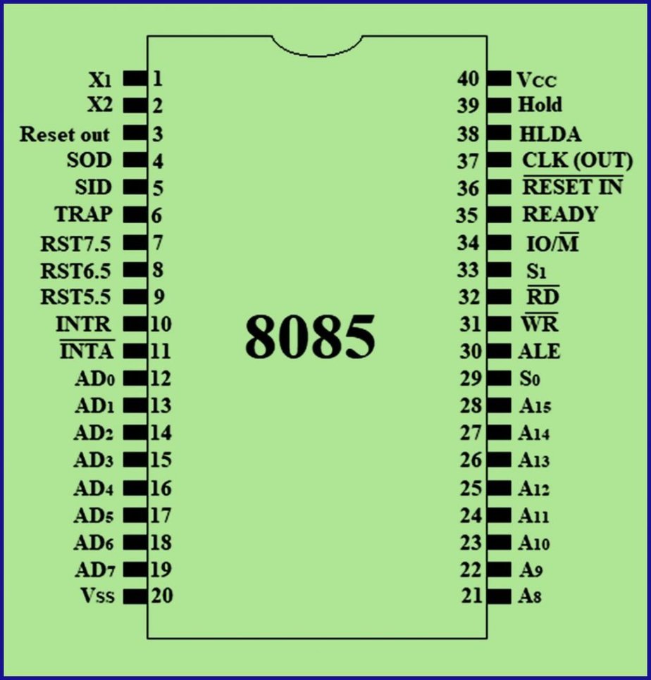
  • 8085 Pin Diagram
  • Working of different pins

Introduction to 8085 Microprocessor:

8085 Microprocessor

The 8085 is an 8-bit programmable microprocessor chip which was first designed by INTEL in the year 1977 utilizing NMOS transistors.

The main features of 8085 microprocessor are:

  • This has total 40 pin.
  • Clock (CLK) speed frequency 3-5 MHz
  • The 8085 microprocessor is equipped with sixteen address lines, and eight data lines. So, 8085 is termed an 8 bit microprocessor depending upon its database.
  • Requires +5V supply to operate.

BUS Architecture of 8085 Microprocessor:

Various I/O devices & memory device are connected to a CPU by group of lines or wires, these are called BUS.

There are three categories of BUS:

ADDRESS BUS 

  • When the address is sent by CPU, all devices are connected to CPU through address BUS and receives this address but only the device will respond which also receives chip enable signal from CPU. Address BUS is Unidirectional.

DATA BUS

  •  It carries data values from microprocessor through a memory cell or a peripheral part (memory or I/O write / memory or I/O read). Data BUS is Bidirectional. So, information flows in both way between 8085 microprocessor & memory or I/O device.

CONTROL BUS

  •  It carries control signal in between Central Processing Unit, memories Input / Output devices. It is also Bidirectional.
1 2
2 3

I/O M̅When the signal is high (logic 1) then CPU wants to communicate with I/O device but when signal goes low (logic o) then CPU will communicate with memory.

R̅D̅ – When CPU sends a low R̅D̅ signal the activated device understands that CPU wants to read information from another device or memory.

W̅R̅T̅ – When CPU sends a low W̅R̅T̅ signal the activated device understands that CPU wants to write information to memory or another device.

What is OPCODE & OPERAND?

OPCODE:

An OPCODE is a signal instruction that can be executed through CPU, without help of opcode any instruction cannot be defined individually.

Example – MOV A, B

Here, MOV means Move, so MOV is OPCODE.

OPERAND:

OPERAND describes an operation such that add, sub, mov on which the operations have to be performed.

Example – MOV A, B

Here, the content of REG B moves to the content of REG A.

Read more about Important Peripherals of 8085 Microprocessor

What are the different sections of 8085 Microprocessor?

There are three categorical area in the 8085 microprocessor;

ALU:

  • This section performs the operation of subtraction, addition of logical NOR, compliment, right shifts, left shifts etc.

REGISTER:

  • Registers are used for temporary storage of data insertion; it has following register,
  • 8 BIT accumulator
  • 8 BIT General Purpose Register (B-C, D-E, H-L)
  • One 16 BIT Stack Pointer
  • One 16 BIT Program Counter
  • Instruction Reg, Status Reg, Temporary Reg

TIMING & CONTROL:

  • These is primarily responsible for the time & control signal generation which are utmost essential for completing the instruction operation. It can control the data flow between CPU & peripheral device & it provides the timing signal for the operation of memory & I/O devices.

Examples of instructions:

  • 1 BYTE Instruction – MOV B, C
  • 2 BYTE Instruction – MVI B, 05
  • 3 BYTE Instruction – LHLD 5000H

PIN Diagram of 8085 Microprocessor: 

The below image represents description of PINS of a 8085 microprocessor.

PIN Diagram of 8085 Microprocessor
PIN Descriptions of 8085 Microprocessor
I/O M̅S1S0OPERATION
000Halt
001Memory write
010Memory read
011Fetch
100Halt
101I/O write
110I/O read
111Fetch
4 2

Descriptions of the Pins of 8085 Microprocessor:

A8 – A15:

  • These address buses are used to be most significant bits of the memory address of 8 bit I/O device.

AD0 – AD7:

  • When the address is multiplexed with the data then it is called AD Bus. The lower order or low significant bus as well as the data bus are used for memory address or I/O address.

ALE

  • The ALE pin is activated for the first cycle & enable to lower 8 bit of the address data bus to be latched (logic 0) & when ALE is logic 1 then address bus is activated.
I/O M̅S1S0OPERATION
000Halt
001Memory write
010Memory read
011Fetch
100Halt
101I/O write
110I/O read
111Fetch

I/O M̅:

  • It is a status signal for memory as I/O device. When the signal goes high it operates for all I/O devices. When the signal goes low, it works for memory.

R̅D̅:

  • It is a signal to control read operation; when the signal is low then it reads the data from I/O device or O/P device.

W̅R̅T̅:

  • It is the specified write control signal. This signal specifies the data on the data bus will be written into a designated memory or I/O device.

READY:

  • It is active high I/P control signal. It is employed by µP to identify whereas a peripheral has finished the data transfer or not.

HLDA:

  • This is the hold acknowledgement signal which is used for granting the hold request.

INTERRUPT:

  • TRAP: It has the highest priority over all the interrupts. If any emergency situation comes then it will work.
  • RST 7.5: The next priority after TRAP is RST 7.5
  • RST 6.5: The next priority after RST 7.5 is RST 6.5
  • RST 5.5: The next priority after RST 6.5 is RST 5.5

INTR R:

  • It is an interrupt request used as general purpose interrupt. It has the lowest priority.

I̅N̅T̅A̅:

  • This signal is interrupt acknowledgement; is used to acknowledge all the interrupts.

RESET IN:

  • If the signal on this pin goes LOW, then the device program counter is being set to zero and when it is up it is in reset condition.

RESET OUT:

  • This signal designates the up is being reset and be utilized as to reset a memory device and input output devices.

SID:

  • Serial I/P data is the data line for signal i/p which is loaded into the accumulator’s 7th bit location.

SOD:

  • Serial o/p data is the 7th bit of the accumulator is o/p on the SOD line.

X1 – X2 [clock input]:

  • These are two input perform as a clock input.

CLOCK O/P:

  • The frequency is the same in which process operate.

VCC & GND:

  • VCC is connected to +5V; and GND pin is Grounded.

For more Electronics related article click here

Microcontroller Vs Microprocessor: 7 Facts You Must Know

1 1 300x152 1

C O N T E N T S

  • What is a Microprocessor?
  • Microprocessor Definition
  • What is BIT, BYTE, Nibble and Ward?
  • Hardware of a Microprocessor
  • Block diagram
  • Important features of Microprocessor
  • Characteristics of Microprocessor
  • What is ALU?
  • Differences between ALU and CPU
  • Memory Organization in Microprocessor
  • Types of processors used in a Microprocessor
  • Applications of Microprocessor
  • What is a Microcontroller?
  • Features of Microcontroller
  • Types of Microcontroller
  • Microcontroller vs Microprocessor

What is a Microprocessor?

Microprocessor Definition:

“Microprocessor is a programmable circuit driven register based, multipurpose semiconductor, i.e., manufactured on LSI or VLSI technique. It takes binary instructions from input devices, processes the instruction & outputs the originals and can store the information”.

Microcontroller vs Microprocessor

Hardware of a Microprocessor:

  • It is the interconnection of several peripheral in such a manner, so that it can perform a particular operation.
  • Microprocessor 8085 was found in 1976 & Microprocessor 8086 was found in 1978.

What is BIT?

The possible value of a logical variable which may or not stand for numerical digit of the binary number system is called BITs.

What is BYTE?

In binary number system a group of 8 bit are called BYTE.

                          1 BYTE = 8 BIT

What is Nibble?

A group of 4 BITS are called Nibble.

                          1 Nibble = 4 BIT

What is Ward?

An array of disk which together convey an item of information is called a Ward.

                          1 Ward = 16 BIT

                          1 Long Ward = 32 BIT

                          2 BYTE = 1 Ward

What are the features of Microprocessor 8085?

Characteristics of Microprocessor:

  • It is 40 pin IC.
  • It is NMOS technology, LSI chip.
  • Clock (CLK) speed frequency 3-5 MHz.
  • 8085 has sixteen bit (16) address lines, and eight bit (8) data lines. So, the 8085 is called an 8 bit microprocessor depending upon database.

Microcontroller vs Microprocessor

What are the limitations of microprocessor 8085?

Disadvantages of 8085:

  • Low speed.
  • Low memory capacity.
  • Limited number of GPR (General Purpose Register).
  • Less powerful instruction.

Memory Organization in Microprocessor:

Microcontroller vs Microprocessor: Memory Organisation
Microcontroller vs Microprocessor Image – 1
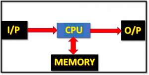
  • Microprocessor is one of the utmost key component of modern computer. It acts as a brain of computer system. A digital computing is a programmable machine. Its main components are i/p, CPU, memory, o/p device.
  • The CPU executes the instruction. The i/p device is used to fetch programme & data to the computer.
  • The memory is the storage device that stores data programme, results etc.
  • The o/p device display programmes, data or results according to their instructions given to the computer. The CPU built on a single IC which is called the MICROPROCESSOR.
  • A digital device in which microprocessor is in case to operate as a CPU is known as MICROCONTROLLER.

Microcontroller vs Microprocessor

Microprocessor Applications:

Microprocessors are widely used in-

  • Different household devices like thermostats, high end coffee makers, washing machines etc.
  • Microprocessor has various industrial applications like cars, boats, heavy machinery, elevators etc.
  • In cell phones, VCR, televisions microprocessor is used numerously.

Types of Microprocessor:

16 BIT Microprocessors-

  • 8086 (Clk speed 4.7 MHz – 10 MHZ);
  • 8088 (Clk speed more than 5 MHz);
  • 80186,80188 (Clk speed 6 MHz);
  • 80286 (Clk speed 8 MHZ);

32 BIT Microprocessors-

  • INTEL 80386 (clk speed 16 MHZ – 33 MHz);
  • INTEL 80486 (clk speed 16 MHz – 100 MHZ);
  • PENIUM (clk speed 66 MHz);

64 BIT Microprocessor-

  • INTEL CORE-2 (clk speed 1.2 GHz – 3 GHz);
  • INTEL i7 (clk speed 3.3 GHz – 66 GHz);
  • INTEL i5 (clk speed 2.4 GHz – 3.6 GHz);
  • INTEL i3 (2.93 GHz – 3.33 GHz);
Microcontroller vs Microprocessor
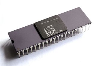
Intel C8086 processor , Microcontroller vs Microprocessor, Image – 2
Photo By – Thomas NguyenIntel C8086CC BY-SA 4.0

Types of processors used in a Microprocessor:

Reduced Instruction Set Computer (RISC) –

An advanced processor circuit consists of RISC architecture. RISC provides improved performance. A RISC has a few addressing modes only. It executes most instructions in a single clock style. Instruction executes by a hardwired implementation. Arithmetic & logic instructions access the operands in multiple register sets, windows or files. This greatly reduces dependency on the external memory accesses for the data.

Complex Instruction Set Computer (CISC) –

CISC has the ability to process complex instructions and complexioned data sets with the smaller number registers and simpler hardwired logic, and use of control memory. CISC be responsible for for a large number of address mode.

CISC may have the addressing modes such as indirect, auto index, index relative addressing modes for the data transfer, logic and arithmetic instructions. Some CISC have reliance on the external memory admittances for data in several addressing modes.

What is ALU?

In computing system, the ALU is a digital circuitry which can perform various mathematical operations.


Differences between ALU and CPU:

 Arithmetic Logic Unit (ALU)Central Processing Unit (CPU)
Full FormALU is the Arithmetic Logic Unit.CPU is Central Processing Unit.
UseALU performs all the arithmetic operations specified to the computer.CPU carries different instructions of a computer program to compute different processes i.e., arithmetic, logical, control & input output operations.
DependenceALU depends on the central unit for the for its functionThe control unit does not depend on anything like ALU.
FunctionsALU takes instructions from control unit and gives result accordingly.Control unit provides instruction to the arithmetic unit to perform.
Microcontroller vs Microprocessor, Table -1

What is a Microcontroller?

Definition of Microcontroller:

“A microcontroller is a device which is made up of microprocessor, Random Access Memory, Read Only Memory, timer, input-output pins and several other device.”

Features of Microcontroller:

Different units of Microcontroller (8051):

  • It has a 12 MHz clock, processor instruction cycle time is 1µs.
  • Microcontroller 8051 has 8 bit arithmetic logic unit.
  • Its internal bus width is 8-bit.
  • It has CISC architecture.
  • Microcontroller 8051 also equipped with a stack pointer.
  • The 8051 equipped with two external interrupt pins, INT0 & INT1.
  • Special Function Register is present in the 8051 microcontroller family.

Block Diagram of Microcontroller:

Microcontroller vs Microprocessor
Microcontroller vs Microprocessor, Image – 3

Types of Microcontroller:

  • PIC Microcontroller;
  • ARM Microcontroller;
  • 8051 Microcontroller;
  • AVR Microcontroller;
  • MSP Microcontroller;
Microcontroller vs Microprocessor
A PIC Microcontroller, Microcontroller vs Microprocessor, Image – 4

Applications of Microcontroller:

Microcontrollers are used widely in-

  • Mobile phones
  • Automobile Industry
  • Cameras
  • Computer Systems
  • Micro Oven etc.

Comparative analysis between Microprocessor and Microcontroller:

Microcontroller vs Microprocessor

     MICROPROCESSOR    MICROCONTROLLER
CPUIt consists of only one CPU.  It consists of a CPU along with memory, I/O all integrated into one chip.
USEMicroprocessor is used in personal computers.Microprocessors are typically used in any of the computational devices or remote controlled systems.
INTERFACEMicroprocessor interfaces are complex.Microcontrollers are straight forward with fewer instructions to execute.
COSTThey are expensiveThey are inexpensive
REGISTERIt has fewer number of register and the operation in it is mainly based on the memory.Here Registers are greater in number. That is why it is more convenient to write programs.
Microcontroller vs Microprocessor, Table – 2


For more Electronics related article click here
51 Important MCQ On Capacitor For Competitive Examination

MCQ2 300x89 1

1. A capacitor has a voltage difference of 10 V across the plates. It has stored charges of 1000 micro-coulombs. What is the capacitance value?

  1. 100 μF
  2. 10 pF
  3. 0.01 μF
  4. 100 pF

Solution: (1). 100 μF.

Answer Hints: We know that capacitance is given as C = Q / V

Q is the amount of charges stored by the capacitor. V is the voltage in between the plates.

Using the equations, we get – C = (1000 * 10 -6) / 10 = 100 μF

Click here for Concept of Capacitor!

2. The plates of parallel plate capacitor is right angle in shape. Two sides of them are 2 cm in size. The distance in between two plate given as: 0.1 cm. What will be the capacitance value if the permittivity of the dielectric is 10-11 F/m?

  1. 1 x 10-14 F
  2. 2 x 10-12 F
  3. 2 x 10-14 F
  4. 1 x 10-12 F

Solution: (2). 2 x 10-12 F. Try to solve without using the hints!.

Answer Hints: The formula of capacitance is given as-

C =ε A/ d

Here C is the capacitance, ε Refers to the medium’s permittivity. d is the distance. The side of the triangles is – 2cm or 0.02m.

The surface area= ½ * 0.02 * 0.02 = 2×10⁻⁴

ε = 10-11 F/m d = 0.001m

So, C = 2 x 10-12 F

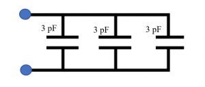
3. Find out the equivalence capacitance.

Capacitors problem 1
Figure – 1
  1. 1/3 pF
  2. 1 pF
  3. 3 pF
  4. 9 pF

Solution: (4). 9pF.

Answer Hints: As we can see that The connection is in parallel..

The equivalent parallel capacitance is stated as Ceq = C1 + C2 + C3 + … + CN

So, the equivalent capacitance is = 3+3+3 = 9 pF

4. Find out the equivalence capacitance of the circuit.

Capacitors problem 2
Figure – 2
  1. 1/3 pF
  2. 1 pF
  3. 3 pF
  4. 9 pF

Solution: (2). 1 pF.

Answer Hints: As we can see, the capacitors are in series connection.

The equivalent series capacitance is stated as 1 / Ceq = 1 / C1 + 1 / C2 + 1 / C3 + … + 1 / CN

So, the equivalent capacitance is = 1 / (1 / 3+1 / 3+1 / 3) = 3/3 = 1 pF

5. A capacitor has a capacitance value of 1 micro-farad. What does it imply?

  1. It stores one coulomb of charge
  2. It holds 6.24 x 10¹² electrons
  3. It stores one volt
  4. It stores one A of current

Solution: (2). It holds 6.24 x 10¹² electrons.

6. What is the effect on capacitive reactance values if the capacitors are connected in series?

  1. An increase in total Xc
  2. A decrease in real Xc
  3. No change in real Xc
  4. Reactance does not depend on connectivity.

Solution: (1). An increase in total Xc

7. How an electrostatic field varies if the charge difference is given?

  1. Plate differential
  2. Plate Distance
  3. Dielectric Quantity
  4. Plate Area

Solution: 4). Plate Area

8. How the capacitance of a parallel plate capacitor can be decreased?

  1. Increasing the gap between the plates
  2. If the charge of the capacitor is increased.
  3. Decreasing the gap between the plates
  4. If the charge of the capacitor is decreased.

Solution: (1). Increasing the gap between the plates

9. A capacitor and an output resistor are connected in series. The circuit will function like –

  1. Bridge Rectifier
  2. Band-stop filter
  3. Low pass filter
  4. High pass filter

Solution: (4). High pass filter.

10. Which type of material is used between the plates of the capacitor?

  1. Diodes
  2. Materials with high impedance
  3. Plate divider material
  4. Dielectric Material

Solution: (4). Dielectric material.

11.  Which material has the highest dielectric value in the below options?

  1. Mica
  2. Air
  3. Paper
  4. Wood

Solution: (1). Mica

12. What is the phase difference for voltage and current in a capacitor only circuit?

  1. The voltage lead by 90 degrees
  2. The current lead by 90 degrees
  3. The voltage lag by 180 degrees
  4. The voltage and current has no phase differences.

Solution: (2). The current lead by 90 degrees.

13. What is the effect on capacitance if the dielectric constant is decreased?

  1. It remains the same
  2. It increases
  3. It decreases
  4. The capacitor does not function.

Solution: (3). It decreases

14. Which of the following is true about capacitor?

  1. C = Q / V
  2. V = Q * C
  3. C = R * I
  4. Q = I / V

Solution: (1). C = Q / V 

15. What is the S.I. unit of capacitor?

  1. Henry
  2. Ohm
  3. Volt / Amp
  4. Farad

Solution: (4) Farad

16. What is the value of the Q factor of a capacitor?

  1. Q = 1 / RC
  2. Q = 1 / (RC)1/2
  3. Q = 1 / ωCR
  4. Correct option is not given

Solution: (3). 1 / ωCR

17. What is the capacitor’s time constant?

  1. τ0 = 1 / C
  2. τ0 = RC
  3. τ0 = 1/RC
  4. τ0 = C

Solution: (2). τ0 = RC

18. Comment Truth or False based on the sentence given.

Statement: Air can serve as the dielectric for the capacitor.

  1. True
  2. False

Solution: (1). True

19. What is dissipation factor for a ceramic capacitor?

  1. tan δ = ESR * ωC
  2. tan δ = ESR * 1 / C
  3. tan δ = 1 / (ESR * ωC)
  4. tan δ = ESR * C

Solution: (1). tan δ = ESR * ωC

What is dissipation factor? Click to Know!

20. What type of ceramic capacitor provides higher stability?

  1. Class 1 type
  2. Class 2 type
  3. Ceramic Disc Capacitor
  4. MLCC

Solution: (1). Class 1 type

21. Which dielectric is used for tantalum metal?

  1. Tantalum Aluminium Di-Oxide
  2. Tantalum Niobium Phosphide
  3. Tantalum pentoxide
  4. Tantalum phosphide

Solution: (3). Tantalum pentoxide

22. Which type of capacitor has the highest CV product?

  1. Ceramic capacitor
  2. Tantalum electrolytic capacitor
  3. Coupling capacitor
  4. bypass capacitor

Solutions: (2). Tantalum Electrolytic capacitors.

Know everything about Tantalum Electrolytic Capacitors…Click to proceed….

23. What is surge voltage?

  1. The minimum voltage received from the load.
  2. The maximum voltage received from the load.
  3. The maximum peak voltage applied.
  4. The minimum peak voltage applied.

Solution: (3). The maximum peak voltage applied.

24. Comment Truth or False based on the sentence given.

Statement: Capacitors are polarized.

  1. True
  2. False

Solution: (1). True

25. How much energy will be stored in a capacitor if the applied voltage is V?

  1. ½ CV2
  2. ½ CV
  3. CV2
  4. 1/4 CV2

Solution: (1). ½ CV2

How energy is being stored in a capacitor? Click for answer!

26. Condenser is currently known as –

  1. Filters
  2. Rectifiers
  3. Capacitors
  4. Diodes

Solution: (3). Capacitors

27. How the impedance of a capacitor is represented in Laplace transform?

  1. Z(s) = s / C
  2. Z(s) = 1 / sC
  3. Z(s) = 1 / s2C
  4. Z(s) = S2 / C

Solution: (2). Z(s) = 1 / sC

28. What will be the effect of increasing the electrode area of a plate capacitor?

  1. The capacitance remains the same.
  2. The energy stored by the capacitor gets decreased.
  3. The capacitance value gets reduced.
  4. The energy stored by the capacitor gets increased.

Solution: (4). The energy stored by the capacitor gets increased.

29. Which of the following is the symbol for a bipolar dielectric capacitor?

Polarized capacitor symbol 1
1.
capacitor 2 1
2.
Polarized capacitor symbol 3
3.
Kondensator
4.

Solution: (4).

30. Which organization gives the standardization for all electrical components, including capacitors?

  1. IEEE(Institute of Electrical and Electronics Engineers)
  2. NMEA(National Marine Electronics Association)
  3. IEC(International Electrotechnical Commission)
  4. Correct option is not given.

Solution: (3).IEC (International Electrochemical Commission).

31. How quality factor is related with Dissipation Factor?

  1. Q = 1 / tan δ
  2. Q = 1 / tan2 δ
  3. Q = tan δ
  4. Q = 1 / ESR * tan δ

Solution: (1). Q = 1 / tan δ

32. Which type of capacitor provides high volumetric efficiency?

  1. Ceramic Capacitors of Class 1
  2. Ceramic Capacitors of Class 2
  3. Ceramic Capacitors of Class 3
  4. Ceramic Capacitors of Class 4

Solution: (2). Ceramic Capacitors of Class 2

33. How does frequency is related to the capacitance of a capacitor?

  1. An increase in the frequency will cause a increase in the capacitance.
  2. An increase in the frequency will cause a decrease in the capacitance.
  3. Increasing the frequency will not affect the capacitance.
  4. Decreasing the frequency will decrease the capacitance.

Solution: (2). An increase in the frequency will cause a decrease in the capacitance.

34. What is voltage proof for a ceramic capacitor?

  1. The surge voltage
  2. The applied voltage
  3. The load voltage
  4. The rated voltage.

Solution: (4). The rated voltage.

35. When does the resonance occurs in a ceramic capacitor?

  1. When the imaginary parts of the capacitor impedance and admittance cancel each other.
  2. When the imaginary parts of the capacitor impedance and admittance do not exist.
  3. When the imaginary parts of the capacitor impedance have a higher value than admittance.
  4. When the imaginary parts of the capacitor impedance have a lower cost than admittance.

Solution: (1) When the imaginary parts of the capacitor impedance and admittance cancel each other.

36. What is the dielectric absorption for a class 1 ceramic capacitor?

  1. 1% to 3%
  2. 7% to 9%
  3. 0.3% to 0.6%
  4. 0.1% to 0.3%

Solution: (3). 0.3% to 0.6%

37. A capacitor is rated as 105K 240 V. What is the capacitance of the capacitor?

  1. 10 µF
  2. 105 µF
  3. 240 µF
  4. 1 µF

Solution: (4). 1 µF

38. A capacitor is rated as 105M 240 V. What is the capacitor’s tolerance value?

  1. ±10%
  2. ±20%
  3. ±30%
  4. ±40%

Solution: (2). ±20%

39. What is MLCC?

  1. Multipurpose Liquid Ceramic Capacitors
  2. Multipurpose Leakage Ceramic Capacitors
  3. Multi-layer Crystalline Capacitors
  4. Multi-layer Ceramic Capacitors

Solutions: (4). Multi-layer Ceramic Capacitors

40. Which type of capacitor is used in transistor circuits?

  1. Air
  2. Bypass
  3. Paper
  4. Ceramic

Solution: (4). Ceramic

41. Which bridge is used for measuring capacitance?

  1. Wheatstone Bridge
  2. Schering Bridge
  3. Both (A) and (B)
  4. Correct option is not given.

Solution: (2). Schering Bridge

42. Which type of capacitor has a short shelf life than others?

  1. Electrolytic Capacitor
  2. Ceramic Capacitor
  3. Both (A) and (B)
  4. None of the above

Solution: (1). Electrolytic Capacitor

43. Which type of capacitor is useful in high-frequency circuits?

  1. Ceramic capacitors
  2. Mica Capacitors
  3. Bypass Capacitors
  4. Air Capacitors

Solution: (2). Mica capacitors

44. Which type of capacitor is used in R.F. tuning?

  1. Ceramic Capacitor
  2. Parallel Plate Capacitors
  3. Electrolytic capacitors
  4. Mica Capacitors

Solution: (3). Electrolytic capacitors

45. Which type of capacitor is used for D.C. voltage?

  1. Ceramic Capacitor
  2. Parallel Plate Capacitors
  3. Electrolytic capacitors
  4. Mica Capacitors

Solution: (3). Electrolytic capacitors

46. Where does the electric charge is stored in a capacitor?

  1. The Dielectric Material
  2. The parallel Plates
  3. Correct option is not given.
  4. Both (A) and (B)

Solution: (1). The Dielectric Material

47. Comment Truth or False based on the sentence given.

Statement: Both Electric field and magnetic field are associated with capacitors.

  1. True
  2. False

Solution: (2). False

48. Comment Truth or False based on the sentence given.

Statement: If the voltage across the capacitor is doubled, the energy stored will be doubled.

  1. True
  2. False

Solution: (1). True

49. What is the value of true power inside a capacitor?

  1. More than 0
  2. Equals to 0
  3. Lies in the range of 0 to 1
  4. Correct option is not given

Solution: (2). Equals to 0

50. How many time constants are required to charge a capacitor completely?

  1. 5
  2. 4
  3. 2.5
  4. 2

Solution: (1). 5

Electrolytic Capacitor:Polarity,Types,7 Important Factors

CAPACITOR SERIES EQUIVALENT 1 300x139 1

Points of Discussion

A. Definition of Electrolytic Capacitor and Overview

B. Family Tree of Electrolytic Capacitors

C. Principle of charge

D. Construction of Capacitor

E. Capacitance and volumetric efficiency

F. Electrical characteristics

G. Symbol of capacitor

Electrolytic Capacitor

Definition

“An electrolytic capacitor can be defined as the capacitor which metal ended anodes. This anode creates an insulating oxide layer.”

The insulating oxide layer functions as a dielectric layer of the capacitor. The oxide layer is roofed by concrete, liquid, or gel electrolytes. This roofed part serves as the cathode of the electrolytic capacitor.

Electrolytic Capacitor Polarity

Symbol of capacitor

Electrolytic capacitors have specific symbol. The symbol in the circuit, let us understand which type of capacitor is this.

Electrolytic Capacitor
Symbol
Single ended e caps IMG 5117
Electrolytic Capacitor ,Image Source –ElcapSingle-ended-e-caps-IMG 5117CC0 1.0

A typical Electrolytic capacitor has a higher capacitance-voltage (CV) product per unit volume in comparison to other types. The feeble dielectric layer as well as the broader anode surface helps to achieve that.

Types of Electrolytic capacitors

They have three kinds –

  • Aluminum type Capacitors
  • Tantalum type Capacitors
  • Niobium type Capacitors

This type of capacitor has a large capacitance, which helps them bypass low-frequency signals and store a large number of energies. They find applications in decoupling and filtering circuits.

These types of capacitors are polarized. The reason behind them is their special structure. They must be operated at higher voltages, and more positive voltages should be on the anode and cathode.

The anode of an industrial usable electrolytic capacitor is marked with a plus sign. An electrolytic capacitor can be destroyed by applying a reverse polarity voltage or using an excessive voltage than the rated working voltage. The destruction is hazardous and can create an explosion to fire.

Bipolar electrolytic capacitors is also one of its kind. It can be formed simply by joining two capacitors by connecting anodes to anode and cathode to cathode.

Know about other types of Capacitors & Workings

Family Tree of Electrolytic Capacitors

Electrolytic capacitors have several varieties. The nature of the positive plate and the type of electrolytic used makes the variation. Each of these three types of capacitors uses concrete and non-solid kinds of electrolytes. The tree is shown below –

Electrolytic Capacitor Tree

Principle of charge

This capacitors stores energy just like regular capacitors. It holds power by parting charge in an electrical field in the insulating oxide layer inside the conductors. An Electrolyte is present here, which acts as the cathode. It also forms another electrode of the capacitor.

Construction

These capacitors practice a chemical property of “Valve metals” to create the capacitor. The practice creates a thin layer of oxide when interchanges with a certain type of electrolyte. There are three solid kinds that are practiced as anode in these capacitors.

1. Aluminium – This type of capacitors uses a high purity imprinted aluminium foil with aluminium oxide as the dielectric material.

2. Tantalum – This type of capacitors use tantalum dust which has lowest level of doping.

[ Read About Tantalum Capacitor. Click Here! ]

3. Niobium – This type of capacitors uses a niobium dust pellet which has lowest level of doping.

The property of the anode materials can be studied below –

MaterialDielectric MaterialStructure of oxidePermittivityBreakdown Voltage(V/µm)
AluminumAluminum Oxide [Al2O3]Amorphous9.6710
AluminumAluminum Oxide [Al2O3]Crystalline11.6-14.2800-1000
TantalumTantalum pentoxide [Ta2O5]Amorphous27625
NiobiumNiobium pentoxide [Nb205]Amorphous41400
Property Table of Anode Materials

We can see that the permittivity of tantalum oxide is three-time more than Aluminium oxide.

Every anode is imprinted with less smooth cover area and has a larger cover area compared to a smothering one. This is done to increase the capacitance per unit volume of the capacitor.

If a positive valued potential is applied across the capacitor’s anodes, a thick oxide barrier layer will be formed. The thickness of the coating area depends upon the applied voltage over the anodes. This oxide layer which is insulator as well, then functions as a dielectric material. The oxide layer generated by the anode can be destroyed if the applied voltage’s polarity is reversed.

After the dielectric formation, a counter needs to match the rough insulating area on which the oxide formed. As the electrolyte acts as a cathode, it accomplishes the matching process.

Electrolytes are categorized mainly in two sections – ‘Solid’ and ‘Non-Solid.’ Liquid mediums with ion conductivity by moving ions are considered non-solid electrolytes. This type of electrolytes can be easily fit on a rough surface. Solid ones work in the rugged structure by using chemical processes like – polymerization for conducting polymers or pyrolysis for manganese dioxide.

Electrolytic Capacitors Capacitance and volumetric efficiency

The working principle of an electrolytic types capacitor is similar as the working of ‘plate capacitor.’

Capacitance is represented by the following equation.  

C = ε*(A /d)

Here,

C is the capacitance.

A is the area of the plates.

d is the distance between two plates.  

ε is the Permittivity of the medium between two plate.

Increasing the electrode area and the dielectric permittivity will increase the Capacitance.

If we look in detail, an electrolytic types capacitor has a weak dielectric layer, and it stays in the boundary of nanometre per volt. There is another reason behind the higher capacitance. It is the rough surface area.

Electrical characteristics

Series equivalence circuitry

The characteristics of electrolytic capacitors is well defined in ‘International generic description IEC 60384-1’. The capacitors can be represented as a flawless corresponding circuit with series connection of electrical components, including all the ohmic losses, capacitive, inductive parameters of an electrolytic capacitor.

The below circuit represents the series equivalent of Electrolytic Capacitors

CAPACITOR SERIES EQUIVALENT 1
Series Equivalent Circuit, Image by – InductiveloadElectrolytic capacitor model, marked as public domain, more details on Wikimedia Commons

C represent the capacitance value of the capacitor; RESR represents the series equivalent resistance. Losses due to heat and ohmic effects are also taken into considerations. LESL is the corresponding inductance in series and considered as the self-inductance of the electrolytic capacitor. Bleak is the leakage resistance.

The Capacitance, Standard Values, and Tolerances Parameter of Electrolytic Capacitor

The construction of anode and cathode primarily decides the characteristics of an electrolytic capacitor. The capacitance value of a capacitor is dependent on some factors like the temperature parameters and the frequency. Electrolytic capacitors of non-solid types have a property of deviation towards temperatures. It shows more deviation than solid types of electrolytes.

The unit of the capacitance is typically in microfarad (µF).

  • The needed acceptance value of capacitance is determined by the specified applications.
  • Electrolytic capacitors do not require the narrow tolerances.

Ready and Category voltage

Rated voltage of Electrolytic capacitor is defined as the voltage at which the capacitor works with full efficiency. If the capacitor is supplied more than the rated voltage the capacitor gets damaged.

If a capacitor is supplied lower voltage than the rated level, it also effects the capacitor. Applying of lower voltages increase the life of the capacitor. Sometimes it increases reliability for tantalum electrolytic capacitors.

Surge Voltage

Surge voltage is the maximum amount of peak voltage that is supplied to the electrolytic capacitors. It is calculated for the period of the capacitor’s usage in a limited number of cycles.

Transient voltage

Electrolytic capacitors which has Aluminium as material has a tendency to show less sensitivity towards transient voltages.

This condition contents only if the frequency and the energy of the transient is comparatively less.

Reverse voltage

A typical electrolytic capacitor is polarized and, in general, entails the anode electrode voltage to be positive in respect to the cathode voltage.

The reverse voltage is seldom used in fixed AC circuits.

Impedance

A typical capacitor is used as a storage component of electrical energy. Sometimes a capacitor is placed to act as a resistive element in an AC circuit. The major application of an electrolytic capacitor is the decoupling capacitor.

Impedance of a capacitor is given by the AC resistance which is frequency dependent and has phase and magnitude at a specified frequency.

To know more about Capacitor click here
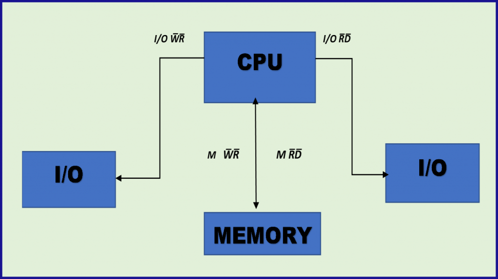
For more Electronics related article click here