23 Facts On Instrumentation Amplifier:The Complete Guide!

Instrument Amplifier

Introduction to Instrumentation Amplifier

An instrumentation amplifier is a particular type of amplifier which is derived from meeting some specific purposes. Instrumentation amplifier provides higher gain, high CMRR (common-mode rejection ratio) and high input impedances. So, we can say that it tries to possess most of the characteristics of an ideal op-amp.

An instrumentation amplifier is often called as In-Amp or InAmp. This article will discuss in detail about circuit, design, formulas, and equations related to the Instrumentation amplifier.

3 Op-Amp Instrumentation Amplifier

A typical Instrumentation amplifier consists of 3 regular op-amps. Two of them are used in a single-stage, whereas the other is used to separate a stage. All three amplifiers work as a differential amplifier, and all of them are connected with negative feedbacks. As instrumentation amplifiers are consisting of 3 amplifiers, they are often called three op-amp amplifier.

Instrumentation Amplifier Circuit

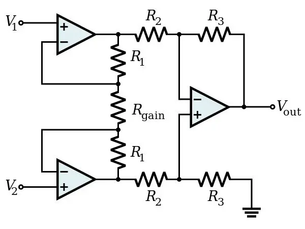
The below image represents a typical circuit diagram of an instrumentation amplifier. Carefully observe the picture as we are going to reference the photo for the rest of the article.

Instrumentation Amplifier

The input voltages are Vi1 and Vi2.

The resistances are R1 (2), R2 (2), R3, R4(2).

The voltage at A and B terminals are VA and VB, respectively.

The current through the R4, R3, and R4 branch is I.

The output of the Amplifier -1 is the Vo1, and that of amplifier -2 is Vo2.

The output of the 3rd amplifier is Vout.

Instrumentation Amplifier Design

An instrumentation amplifier is a combination of 3 typical amplifiers. They are connected in a specific order to build an instrumentation amplifier. We can segregate the instrument amplifier design into two-part.

The first part is “Two input and two output”. Two standard operational amplifiers are connected, as shown in the amplifier circuit figure. Both of them are provided with negative feedback as it stabilizes the circuit more. The output of both the amplifier is connected with three resistors.

The second part is a basic “Differential Amplifier”.  The output of both the previous amplifier acts as input for the last amplifier. Outputs are connected with two identical valued resistors with the amplifier. The positive section is grounded, and negative feedback is associated with the negative terminal and the o/p of this op-amp is the final output of the instrument amplifier.

Instrumental Amplifier Derivation

Let us derive the functional equations and formulas for the instrumentation amplifier. To derive the equations, let us know what happens inside the whole instrument amplifier. As we have previously mentioned, the separation of two stages so, we will calculate it partly.

At the first stage, the input is provided to the non-inverting terminals of both the amplifiers. The amplifier is differential amplifiers.  So, they find out the difference between the given input voltages. Now, refer to the circuit diagram; the input voltages are Vi1 and Vi2. The inverting terminal of the circuit is connected with negative feedback from the output of the amplifiers. Let us say the inverting terminals of both the amplifiers are having potentials VA and VB, respectively. They appear at the node connecting with the resistance lines and branch.

Considering the virtual short-circuit works, the A and B terminal receive the same amount of voltage as the inputs. So, we can say, VA = Vi1, VB = Vi2. The whole stage works like a differential amplifier. That means the difference between the two inputs voltage will be amplified at the output. The output will be again the differences between the two outputs voltage. That can be expressed as follow:

Vo1 – Vo2 = k (Vi1 – Vi2)

Here k is the gain of the amplifier.

At stage two, the difference of the amplifiers is fed as the input for the amplifier. The amplifier at this stage simply works like a typical amplifier. The resistances are connected with the information are of the same values as the differential amplifiers’ requirement. The inverting terminal is associated with the ground, and the amplifier is though of having virtual grounds. In the next section, we will derive the mathematical calculations for an instrument amplifier.

Instrument Amplifier Equation

The input voltages are Vi1 and Vi2.

If the virtual shorting works, then VA = Vi1 and VB = Vi2

Now, there is no current flow from A and B to the resistance branch. There is only a typical current through the branch, and that is current I. ‘I’ is given as:

I = (Vi1 – Vi2) / R3.

The current ‘I’ can also be calculated using the node analysis. It comes as follow.

I = (Vo1 – Vo2) / (R4 + R3 + R4)

Or, (Vo1 – Vo2) = (Vi1 – Vi2) * (R3 + 2R4) / R3

The above equation explains the operation of the first stage. For the second stage, the op-amp’s output is the final output of the instrumentation amplifier.

From the operation of a difference amplifier, we can write that,

Vout = (R2 / R1) x (Vo2 – Vo1)

Or, Vout = (R2 / R1) x (R3 + 2R4) x (Vi1 – Vi2) / R3

This is the instrumentation amplifier equation or the output equation of an instrumentation amplifier. Now, look at the derivation section of this article. Vo1 – Vo2 = k (Vi1 – Vi2). The obtained equation is in the same format.

Instrumentation Amplifier Gain

The amplifier’s gain is referred to as the factor by which the amplifier amplifies the input signal. The resistance values represent the gain of an instrumentation amplifier. The gain also depends on the type of feedbacks being used. The positive feedback provides higher gain, whereas negative feedback provides better stabilities of the system.

The instrumentation amplifier’s general equation is Vo1 – Vo2 = k (Vi1 – Vi2), representing the gain as: ‘k’.

Instrumentation Amplifier Gain Formula

As mentioned earlier, the amplifier gain can be derived from the output equation of the amplifier. The output equation is as follow:

Vout = (R2 / R1) x (R3 + 2R4) x (Vi1 – Vi2) / R3

Comparing this equation with the following equation:

Vo1 – Vo2 = k (Vi1 – Vi2)

We can write,

k = (R2 / R1) x (R3 + 2R4) / R3, this is the instrumentation amplifier gain formula.

Instrumentation Amplifier IC

Typical amplifiers are packaged through Integrated Circuit or ICs. So, if we want to build an Instrumental amplifier using regular op-amps, we have to use op-amp ICs. There is also a separate IC available for Instrumentation amplifiers. There is no need for connecting one op-amp with another. These types of ICs are used commercially where more numbers of ICs are used at a time.

Instrumentation Amplifier Module

Instrumentation amplifiers modules are a combination of a few electronic devices, and the main of them is the Instrumentation Amplifiers. Two of the excellent instrumentation amplifiers are AD623, AD620.

The modules are used explicitly in medical engineering devices of low powers, low power signal amplifier, thermocouples. Some of the characteristics are – a) It provides higher gain, b) Better stability, c) Low power d) High Accuracy.

Instrumental Amplifier IC List

As an instrumentation amplifier can be build using different ICs, we have made a list of all ICs that can be used for Instrumental Amplifiers. The IC numbers are given in the list.

Name of the ICIC SpecificationComments
Instrumentation AmplifierINA128Single-Chip.
Dual Instrumentation AmplifierINA212816 pin IC
Typical Op-AmpLM324IC had four amplifiers.
Instrumentation AmplifierAD623Eight pin IC having a single instrumentation amplifier
Precision Instrumentation AmplifierAD62416 pin IC  
Operational AmplifierIC741Four pin IC and works as a single unit of the op-amp.

Instrumentation Amplifier Load Cell

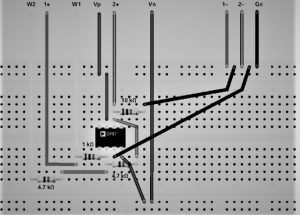
The performance of the instrumentation amplifier gradually increases upon connecting the load cell. The amplifier provides higher CMRR, higher input impedances and thus improves the performance. The detailed connection for the instrumentation amplifier with load cell is shown in the below image.

Instrumentation Amplifier offset voltage

Every op-amp has its offset voltage. The offset voltage is defined as the must need a voltage that must be applied between two inputs to nullify the difference between them and this offset value of every op-amp is specified in the datasheet provided by the manufacturer. For Instrumentation amplifiers, the offset voltage is significantly less, which is desirable.

Instrumentation Amplifier Output Waveform

To observe an instrumentation amplifier’s output, we have to connect it with a CRO (Cathode Ray Oscilloscope). We provide input as sine waves as two input signals, and work is measured from the last amplifier. Co-axial probes are connected with the pins to observe the output waveform. The below image depicts the output. The output is the amplified difference between the applied input voltages.

Instrumentation amplifier and analog multiplier waveforms Channel 1 INA output Channel
Output Waveform

Instrumentation Amplifier transfer function

The transfer function of a system refers to the process which describes or provides output for each input. As the amplifier takes two inputs and amplifies them, the transfer function will reflect the same. The transfer function can be written as:

Vo1 – Vo2 = k (Vi1 – Vi2)

Here Vi1 and Vi2 are the two inputs, and k is the gain.

Dual Instrumentation Amplifier

A dual instrumentation amplifier is a special kind of instrumentation amplifier having great accuracy. It is designed in a certain way to provide high gain, greater accuracy from a minimal size of IC. It also has a low offset voltage. For a wider bandwidth and a connected external resistor, the dual amplifier can provide gain up to 10,000.

The INA2128 IC is used as a dual instrumental amplifier. Some of the significant Applications of dual instrumentation amplifier are sensor amplifiers, medical engineering devices, and battery-operated equipment.

Instrumentation Amplifier vs Operational Amplifier

Points of ReferenceOperational AmplifierInstrumentation Amplifier
Basic StructureBuild up of Bipolar Junction Transistors or Metal Oxide Field-Effect Transistors.The buildup of three Differential Amplifiers
GainNormal GainHigher Gain
Buffer ConnectionAn operational amplifier can be used to make a buffer circuit.A buffer circuit is a part of the whole circuit.
IC specificationIC741AD623

Instrumentation Amplifier advantages and disadvantages

Instrumentation Amplifiers is developed to gain more advantages over typical differential amplifiers. That is why instrumentation amplifiers are used in most commercial applications. But it has some advantages too. Let us discuss some of the instrumentation amplifiers advantages and disadvantages.

Advantages

1. Accuracy and Precision in Measurement: Instrumentation amplifiers are used for testing and measurement purpose. Instrument amplifiers don’t need to match the input impedances. That is why they are so useful for testing. The better parametric values like higher CMRR, high input impedance also gain advantages.

2. Gain: Instrumentation amplifiers provide greater values for open-loop gain. It is a clearer advantage which is also an essential requirement for the amplifiers.

3. Stability of the System: Inside the Instrumentation Amplifiers, all normal op-amps are connected in negative feedback. As we know, negative feedback stabilises the system; the Instrumentation amplifier’s stability is also high.

4. Scalability: Instrumentation amplifiers are incredibly scalable. It provides the option to scale the signal at the input level. That is why the overall amplification is much greater than other amplifiers. The range for scaling is high for that reason also.

5. Accessibility: Instrumentation amplifiers come in ICs. There are eight-pin ICs are available. So, it is easier to handle and use. Also, there are not many factors to take during the amplification. The user just has to know the input signal well. Let us find the disadvantages of the instrumentation amplifiers.

Disadvantages

1. The Instrumentation amplifier suffers from the issue of long-range transmission. The amplifier tends to mix up the original signals with the noises if the input signal is sent for an extended range for communication. The issue can be resolved if the cable type can be improvised so that the noise gets cancelled at the primary stage or no noise enters the transmission line.

Instrumentation Amplifier Characteristics

Let us look at the characteristics of the instrumentation amplifiers at a glance.

  • Instrumentation Amplifiers are Differential Amplifiers made up of three op-amps.
  • It provides a higher open-loop gain than typical op-amps.
  • It has higher CMRR, higher input impedance, low offset voltages, lower output impedances, making it close to the ideal op-amp.
  • Instrumentation amplifiers provide higher accuracy and precision when used in testing and measuring.
  • Instrumentation amplifiers are available in ICs for commercial purposes.

2 op amp instrumentation Amplifier

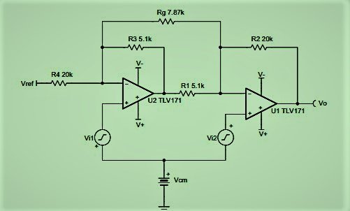
Typical instrumentation amplifiers are made up of 3 amplifiers but it is also possible to make an instrumentation amplifier using a two op-amp. The below image depicts the a 2 op amp based Instrumentation Amplifier Circuit.
Annotation 2021 04 11 135148
Two op-amp Instrumentation Amplifier Circuit

instrumentation amplifier noise analysis

There are particular types of instrumentation-amplifiers available for measuring the weakest signal in a noisy environment. They are known as noise instrumentation-amplifiers. These types of instrumentation amplifiers are used for noise analysis.

Instrumentation amplifier for current sensing

Separate current sensing amplifiers are available in the market for current sensing. But an instrumentation amplifier can also operate current sensing. The primary difference between the two amplifiers is in the input topology.

Frequently Asked Questions

1. Why use an instrumentation amplifier?

Answer: Instrumentation-amplifiers provide higher gain, higher CMRR, higher input impedances, lower output impedances. Thus, we can observe it possesses very close properties of an ideal op-amp. That is why an instrumentation-amplifier is used.

2. When to use an instrumentation amplifier?

Answer: Instrumentation-amplifiers are required every time the user requires a higher gain with better stability of the system to amplify a signal. If the user needed very accurate testing results and measurements, then the instrumentation amplifier comes as a solution.

3. What is an Instrumentation amplifier for load cell?

Answer: The performance of the instrumentation-amplifier gradually increases upon connecting the load cell. The amplifier provides higher CMRR, higher input impedances and thus improves the performance. The detailed connection for the instrumentation amplifier with load cell is shown in the below image. (Point to be noted – Connect all the ground.

4. What is a circuit diagram of an instrumentation amplifier for a biosignal with a gain of a thousand?

Answer: The standard connection of the instrumentation-amplifier provides a specific gain. But adding up an external resistor will give you a boost of thousand.

5. What is the working principle of an instrumentation amplifier?

Answer: The working principle of the instrumentation amplifier is the same as that of a Differential amplifier. It takes the input voltages and amplifies the difference to provide that amplified difference as the output.

Basically: Output = Gain * (Input1 – Input2)

6. What are the advantages of using an instrumentation amplifier over an ordinary differential amplifier in measuring low signals and voltages?

Answer: The advantages are –

  • Accuracy and Precision in Measurement: Instrumentation amplifiers are used for testing and measurement purpose. Instrument amplifiers don’t need to match the input impedances. That is why they are so useful for testing. The better parametric values like higher CMRR, high input impedance also gain advantages.
  • Gain: Instrumentation amplifiers provide greater values for open-loop growth. It is a more clear advantage which is also an essential requirement for the amplifiers.
  • Stability of the System: Inside the Instrumentation Amplifiers, all normal op-amps are connected in negative feedback. As we know, negative feedback stabilises the system; the Instrumentation amplifier’s stability is also high.
  • Scalability: Instrumentation amplifiers are incredibly scalable. It provides the option to scale the signal at the input level. That is why the overall amplification is much greater than other amplifiers. The range for scaling is high for that reason also.
  • Accessibility: Instrumentation amplifiers come in ICs. There are eight-pin ICs are available. So, it is easier to handle and use. Also, there are not many factors to handle during the amplification. The user has to know the input signal well.

7. Why is CMRR important in instrumentation amplifier?

Answer: CMRR is an essential parameter for measuring the performance of an op-amp. CMRR estimates how much amount of common-mode signal will appear in the output measurement. Instruction Amplifier, being an op-amp explicitly used for measuring and testing purposes, should have the lowest CMRR. It is a basic need for the op-amp; otherwise, it will affect the measurement.

8. What is the difference between an instrumentation amplifier and an inverting adder using two op-amps?

Answer: The difference will be in workings and as well as in the parametric values. Inputs for an instrumentation amplifier is never supplied in the inverting terminals. So, there will be changes. Also, the instrumentation amplifiers have buffer circuits, and the feedbacks of them are negative feedback which increases the system’s stability. So, there are massive deviations from the actual results.

9. What is the purpose of a buffer within an instrumentation amplifier?

Answer: The buffer inside the instrumentation amplifier is helpful in many ways. The buffer increases the input impedance, which is very necessary. It also eliminates the difference between two input voltages; thus, the offset voltage value gets decreased. It also affects the CMRR.

10. What are good rules of thumb for building instrumentation amplifiers?

Answer: There is no such hard and fast rules for designing or building instrumentation amplifiers. But there are some best practices. Some of them are – a) Design the circuit symmetrically, b) Implement the gain in the first stage, c) Considers the factors of CMRR, thermocouple effects and resistance values, d) Design the second stage.

11. How to remove offset voltage in the instrumentation amplifier?

Answer: The offset voltage of any amplifier is removable by feeding an adjustable current from a voltage source. A high-valued resistor should be placed between the current and the op-amp.

For more Electronics related article click here
Op-Amp As Integrator & Differentiator : Beginner’s Guide!

differentiator

Contents

  • What is Integrator?
  • Working principle of Integrator
  • Op-amp integrator circuit
  • Output of an integrator
  • Derivation of Op-amp as integrator
  • Practical op-amp integrator
  • Applications of integrator
  • What is Differentiator ?
  • Op-amp as Differentiator
  • Working Principle of Differentiator
  • Output waveform of a differentiator
  • Applications of Differentiator

What is Integrator?

Definition of Integrator

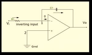
If the feedback path is made through a capacitor instead of a resistance , an RC Network has been established across the operational amplifiers’ negative feedback path. This kind of circuit configuration producing helps in implementing mathematical operation, specifically integration, and this operational amplifier circuit is known as an Operational amplifier Integrator circuit.

The output of the circuit is the integration of the applied input voltage with time.

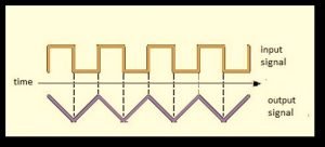
Integrator circuits are basically inverting operational amplifiers (they work in inverting op-amp configuration, with suitable capacitors and resistors), which generally produce a triangular wave output from a square wave input. Hence, they are also used for creating triangular pulses.

Op-amp as Integrator

Working principle of Integrator

Operational amplifiers can be used for mathematical applications such as Integration and Differentiation by implementing specific op-amp configurations.

When the feedback path is made through a capacitor instead of a resistance , an RC Network has been established across the operational amplifiers’ negative feedback path. This kind of circuit configuration producing helps in implementing mathematical operation, specifically integration, and this operational amplifier circuit is known as an Operational amplifier Integrator circuit. The output of the circuit is the integration of the applied input voltage with time.

Op-amp integrator circuit

Integrator Circuit
Op-amp integrator circuit

Output of an integrator

Input Output of Integrator
input and output waveform of an integrator

Integrator circuits are basically inverting operational amplifiers (they work in inverting op-amp configuration, with suitable capacitors and resistors), which generally produce a triangular wave output from a square wave input. Hence, they are also used for creating triangular pulses.

The current in the feedback path is involved in the charging and discharging of the capacitor; therefore, the magnitude of the output signal is dependent on the amount of time a voltage is present (applied) at the input terminal of the circuit.

Derivation of Op-amp as integrator

As we know from the virtual ground concept, the voltage at point 1 is 0V. Hence, the capacitor is present between the terminals, one having zero potential and other at potential V0. When a constant voltage is applied at the input, it outcomes in a linearly increasing voltage (positive or negative as per the sign of the input signal) at the output whose rate of change is proportional to the value of the applied input voltage.

From the above circuitry it is observed, V1 = V2 = 0

The input current as:

aaa

Due to the op-amp characteristics (the input impedance of the op-amp is infinite) as the input current to the input of an op-amp is ideally zero. Therefore the current passing from the input resistor by applied input voltage Vi has flown along the feedback path into the capacitor C1.

Therefore the current from the output side can also be expressed as:

aaaa

Equating the above equations we get,

aaaaa

Therefore the op-amp output of this integrator circuit is:

b

As a consequence the circuit has a gain constant of -1/RC. The negative sign point toward an 180o phase shift.

Practical op-amp as aintegrator

If we apply a sine wave input signal to the integrator, the integrator allows low-frequency signals to pass while attenuates the high frequencies parts of the signal. Hence, it behaves like a low-pass filter rather than an integrator.

The practical integrator still has other limitations too. Unlike ideal op-amps, practical op-amps have a finite open-loop gain, finite input impedance, an input offset voltage, and an input bias current. This deviation from an ideal op-amp can affect working in several ways. For example, if Vin = 0, current passes through the capacitor due to the presence of both output offset voltage and input bias current. This causes the drifting of the output voltage over time till the op-amp saturates. If the input voltage current is zero in case of the ideal op-amp, then no drift should be present, but it is not true for the practical case.

To nullify the effect caused due to the input bias current, we have to modify the circuit such that Rom = R1||RF||RL

In this case, the error voltage will be 

bb

Therefore the same voltage drop appears at both the positive and negative terminals because of the input bias current.

For an ideal op-amp operating in the dc state, the capacitor performs as an open circuit, and hence, the gain of the circuit is infinite. To overcome this, a high resistance value resistor RF is connected in parallel with the capacitor in the feedback path. Because of this, the gain of the circuit is limited to a finite value (effectively small) and hence gets a small voltage error.

bbb
Practical Integrator
practical op-amp integrator
  • VIOS refers to the input offset voltage
  • IBI refers to the input bias current

What is Differentiator ?

Definition of Differentiator

If the input resistance in the inverting terminal is replaced by a capacitor, an RC Network has been established across the operational amplifiers’ negative feedback path. This kind of circuit configuration helps in implementing differentiation of the input voltage, and this operational amplifier circuit configuration is known as an Operational amplifier differentiator circuit.

An operational amplifier differentiator basically works as a high pass filter and, the amplitude of the output voltage produced by the differentiator is proportionate to the change of the applied input voltage.

Op-amp as a Differentiator

As we have studied earlier in the integrator circuit, op-amps can be used for implementing different mathematical applications. Here we will be studying the differential op-amp configuration in detail. The differentiator amplifier is also used for creating wave shapes and also in frequency modulators.

An operational amplifier differentiator basically works as a high pass filter and, the amplitude of the output voltage produced by the differentiator is proportionate to the change of the applied input voltage.

Working Principle of Differentiator

When the input resistance in the inverting terminal is replaced by a capacitor, an RC Network has been established across the operational amplifiers’ negative feedback path. This kind of circuit configuration helps in implementing differentiation of the input voltage, and this operational amplifier circuit configuration is known as an Operational amplifier differentiator circuit.

In a differentiating op-amp circuit, the output of the circuit is the differentiation of the input voltage applied to the op-amp with respect to time. Therefore the op-amp differentiator works in an inverting amplifier configuration, which causes the output to be 180 degrees out of phase with the input. Differentiating op-amp configuration generally responds to triangular or rectangular input waveforms.

A Differentiator Circuit

differentiators
Op-amp differentiator circuit

As shown in the figure, a connection of capacitor in series with the input voltage source has been made. The input capacitor C1 is initially uncharged and hence operate as an open-circuit. The non-inverting terminal of the amplifier is connected to the ground, whereas the inverting input terminal is through the negative feedback resistor Rf and connected to output terminal.

Due to the ideal op-amp characteristics (the input impedance of the op-amp is infinite) as the input current, I to the input of an op-amp is ideally zero. Therefore the current flowing through the capacitor (in this configuration, the input resistance is replaced by a capacitor) due to the applied input voltage Vin flows along the feedback path through the feedback resistor Rf.

As observed from the figure, point X is virtually grounded (according to the virtual ground concept) because the non-inverting input terminal is grounded (point Y is at ground potential i.e., 0V).

Consequently, Vx = Vy = 0

With respect to the input side capacitor, the current carrying through the capacitor can be written as:

cc

With respect to the output side feedback resistor, the current flowing through it can be represented as:

ccc

From the above equations when we equate the currents in both the results we get,

cccc
ccccc

The differentiating amplifier circuit requires a very small time constant for its application (differentiation), and hence it is one of its main advantages.

The product value C1Rf is known as differentiator’s time constant, and output of the differentiator is C1Rf times the differentiation of Vin signal. The -ve sign in the equation refers that the output is 180o difference in phase with reference to the input.

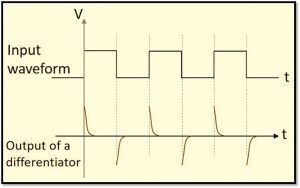
When we apply a constant voltage with one step change at t=0 like a step signal in the input terminal of the differentiator, the output should be ideally zero as the differentiation of constant is zero. But in practice, the output is not exactly zero because the constant input wave takes some amount of time to step from 0 volts to some Vmax volts. Therefore the output waveform appears to have a spike at time t=0.

Output Spike
Output waveform Containing spike

Therefore for a square wave input, we get something like shown in the below figure,

Output waveform
Output waveform of a differentiator for a square wave input

For more Electronics related article and their detail explanation  click here

.

7 Facts On Log & Antilog Amplifier:What,Working,Circuit,Use

log amplifier Symbol 300x154 1

The operational amplifier circuit configurations which can perform mathematical operations such as log and antilog (exponential), including an amplification of the input signal provided to the circuit, are known as Logarithmic amplifier and Antilogarithmic amplifier respectively. In this section, we are going to learn about the Logarithmic amplifier and Antilog in detail.

Contents:

  • Introduction
  • Logarithmic (Log) Amplifier
  • Log amplifier configuration
  • Diode based Log amplifier configuration
  • Transistor based Log amplifier configuration
  • Output and Working Principle of Log Amplifier
  • Applications of the log amplifier
  • What is Antilog?
  • Antilog Amplifier
  • Log amplifier configuration
  • Diode based antilog amplifier configuration
  • Transistor based antilog amplifier configuration
  • Output and Working Principle of Log Amplifier
  • Applications of the antilog amplifier

Logarithm (Log) Amplifier

An operational amplifier in which the output voltage of the amplifier (V0) is directly proportional to the natural logarithm of the input voltage (Vi) is known as a logarithmic amplifier. Basically, the natural logarithm of the input voltage is multiplied by a constant value and produced as output.

Log Amplifier Circuit

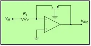
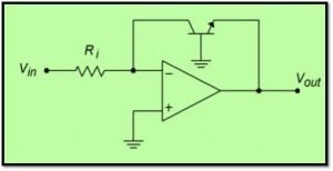
Log Amplifier Using Transistor

Log amplifier
Log amplifier using Transistor

Log Amplifier using Diode

Log amplifier
Log amplifier using Diode

Output and Working Principle of Log Amplifier

This can be expressed as follows:

image002 2

Where K is the constant term, and Vref refers to a normalization constant, which we get to know in this section.

Generally, logarithm amplifiers may require more than one op-amp, in which case they are known as compensated logarithm amplifiers. They even require high performing op-amps for their proper functioning, such as LM1458, LM771, and LM714, are being some of the widely used logarithm amplifier.

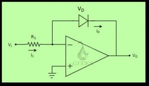
The diode is connected in forward biasing. So, the diode current can be represented as:

image003 6

Where Is is the saturation current, VD is the voltage drop for the diode. The  VT is the thermal voltage. The diode current can be rewritten with high biasing condition,

image005 8

The i1 expressed by,

image007 9

Since the voltage at inverting terminal of the op-amp is at virtual ground, hence, the output voltage is given by V= -VD

Noting that i= iD, we can write

image010 3

But, as noted earlier, VD = -V0 and so,

image013 8

Taking natural logarithm on both sides of this equation, we found

image015 7

Or,  

image018 3                      

The equation of the output voltage (V0) of the logarithm amplifier contains a negative sign, which indicates that there is a phase difference of 180 o. Or, 

 image019 4                                                                       

A more advanced one utilize bipolar transistors to remove Is in the logarithmic term. In this type of logarithm amplifier configuration, the output voltage is given as:

image021 3

Applications of the logarithmic amplifier

Log amplifier is used for mathematical applications and also in different devices as per their need. Some of the applications of the log amplifier are as follows:

  • Log amplifiers are used for mathematical applications, mainly in multiplication. It is also used in the division and other exponential operations too. As it can perform multiplication operation, hence it is used in analog computers, in synthesizing audio effects, measuring instruments that require multiplication operation such as in calculating power (multiplication of current and voltage).
  • As we know that when we need to calculate the decibel equivalent of a given quantity, we require the use of a logarithmic operator, and hence, log amplifiers are used to calculate decibel (dB) value of a quantity.
  • Monolithic logarithmic amplifiers are used in certain situations, like in Radio Frequency domain, for efficient spacing (reducing components and space needed by them), and also to improve bandwidth and noise rejection.
  • It is also used in different ranges of applications such as rot mean square converter, an analog-to-digital converter, etc.

What is Antilog?

Antilog Amplifier

An Op-amp in which the output voltage of the amplifier (V0) is directly proportionate to the anti-log of the input voltage (Vi) is known as an anti-logarithmic amplifier or anti-log amplifier. Here, we are going to discuss the operational amplifier configuration that forms the anti-logarithmic amplifier in detail.

Antilog Amplifier Circuit

Antilog Amplifier Using Transistor

Antilog
Antilog Amplifier using Transistor

Antilog Amplifier using Diode

In the antilog amplifier, the input signal is at the inverting pin of the operational amplifier, which passes through a diode.

Antilog
Antilog Amplifier using Diode

Output and Working Principle of Antilog Amplifier

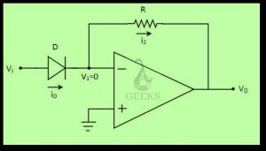
As observed in the circuit shown above, the negative feedback is achieved by connecting the output to the inverting input terminal. According to the concept of the virtual ground between the input terminals of an amplifier, the voltage V1 at the inverting terminal will be zero. Because of ideally infinite input impedance, the current flowing through the diode due to the applied input voltage in the inverting terminal will not enter the op-amp; instead, it will flow along the feedback path through the resistor R as shown in the figure.

The compliment or inverse function of the logarithmic amplifier is ‘exponential’,  anti-logarithmic or simply known as ‘antilog’. Consider the circuit given in the figure. The diode current is

image005 8

Where, VD is the diode voltage. According to the concept of virtual ground, V1=0 as the non-inverting terminal is grounded as shown in the figure. Therefore the voltage across the diode can be expressed as V= V– V1 or VD = Vi Hence, the current through the diode is

image025 2

Due to the ideal characteristics of an op-amp (infinite input impedance), the current flowing through the diode ( iD) flows along the feedback path through the resistor R, as we can observe in the figure.

Therefore i= i2

And, V0 = -i2R = -iDR

Replacing iD in the above equation we get 

image027 3

The parameters n, VT and Iare constants (they are only depend on the diode characteristics which are always constant for a particular diode). Therefore if the value of the feedback resistor R is fixed, then the output voltage V0 is directly proportional to the natural anti-logarithm (exponential) of the applied input voltage Vi. The above equation then can be simply represented as

 image031 3

Where K = – ISR and a = image033 1

Therefore we can notice that the anti-logarithmic op-amp produces its output signal as the exponential value of the input voltage signal applied.

The gain of the anti-log amplifier is given by the value of K that is equal to -ISR.

The –ve sign point out that there is a phase difference of 180degrees between the applied input s and the output of the anti-log amplifier.

For more Electronics related article click here

33 Facts On Summing Amplifier:Inverting, Non-Inverting

Summing amplifier breadboard circuit 2 300x215 1
  1. summing operational amplifier
  2. summing amplifier definition
  3. non inverting summing amplifier
  4. inverting summing amplifier
  5. summing amplifier circuit
  6. inverting summing amplifier circuit
  7. non inverting summing amplifier circuit
  8. summing amplifier with ac and dc input
  9. summing amplifier output
  10. summing amplifier waveform
  11. summing amplifier output waveform
  12. gain of a summing amplifier
  13. determine the output voltage of the summing amplifier
  14. summing amplifier derivation
  15. inverting summing amplifier formula
  16. non inverting summing amplifier derivation
  17. summing amplifier gain formula
  18. summing amplifier ic
  19. summing amplifier schematic
  20. analog summing amplifier
  21. summing and difference amplifier theory
  22. audio summing amplifier
  23. current summing-amplifier
  24. difference between inverting and non inverting summing amplifier
  25. digital to analog converter summing-amplifier
  26. function of summing amplifier
  27. single supply summing-amplifier
  28. summing-amplifier applications
  29. summing amplifier audio mixer
  30. summing amplifier dc offset
  31. summing amplifier design
  32. summing-amplifier example
  33. summing scaling and averaging amplifier
  34. summing amplifier circuit on breadboard
  35.  FAQs

Summing operational amplifier

A summing-amplifier is one of the op-amp applications, which performs summation or addition operations. Multiple input voltages are supplied into the amplifier, and the output provides an amplified summation of the voltages. Summing-amplifiers has various applications in electronics. It also has two types – inverting summing-amplifier and non-inverting summing-amplifier. In detail, we will discuss the analysis of the summing-amplifier in the following article.

summing amplifier
summing-amplifier
Image credit : Wikipedia commons

Summing amplifier definition

A summing-amplifier can be defined as An amplifier, which takes multiple inputs at one of the input terminals and provides the weighted sum of all the inputs.

Non inverting summing amplifier using op amp

Non-inverting summing-amplifier is one of the types of summing-amplifiers. In this type of operations, the input voltages are provided in the amplifier’s non-inverting terminal. The polarity of the output remains the same as the inputs and because of this, it is termed as non-inverting summing-amplifier.

Inverting summing amplifier

Inverting summing-amplifier is another type of summing-amplifier where the input voltages are provided in the inverting terminals. The polarity of the output voltages gets changed and for that reason it is known as inverting summing-amplifier.

Summing amplifier design

A summing-amplifier is designed with the help of a basic op amp and resistances. It can be designed in two main configurations

  • inverting summing-amplifier.
  • non-inverting summing-amplifier.

 We will discuss the general designing of a summing-amplifier.

To design a circuit with an op-amp, we have to keep in mind the op-amp’s basic properties. They are – high input impedance and the concept of virtual ground. For the virtual ground, we have to make a ground connection in any input terminal (the conventional way is to connect the ground in the opposite terminal where inputs are not supplied). A feedback path is created, keeping in mind the high input gain. Generally, a negative feedback path is made for system stability. The Inputs are provided with resistances. The output is collected from the output, containing the weighted sum of input.

Summing amplifier circuit | Op amp summing amplifier circuit design

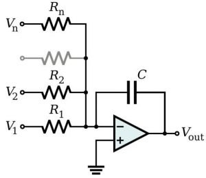
The below images represent circuit diagrams of the summing-amplifier. The first one is for inverting the summing-amplifier circuit, and the second is for the non-inverting summing-amplifier circuit.

Inverting summing amplifier circuit

300px Op Amp Inverting Amplifier.svg
Image by: InductiveloadOp-Amp Inverting Amplifier, marked as public domain, more details on Wikimedia Commons

Non inverting summing amplifier circuit

300px Op Amp Non Inverting Amplifier.svg
Image by: InductiveloadOp-Amp Non-Inverting Amplifier, marked as public domain, more details on Wikimedia Commons

Observe both the circuit diagram as you can observe the difference in applying the input voltages.

Summing amplifier with ac and dc input

A summing-amplifier can be provided with either ac voltage or dc voltage. The input voltage types generally have no in the operation of the amplifier.

Summing amplifier output

The output of a summing-amplifier provides the amplified added up input voltages provided at one of the op amp input terminals. The polarity of the output voltage depends on selecting the input terminal and if the input is provided in the non-inverting terminal, the output will not be inverted. Still, if the input is provided in the inverting terminal of the circuit, there will be a polarity change.

Summing amplifier waveform

The input and output voltages of an op-amp can be observed and measured using a CRO. The CRO pins are connected with the input pins and the ground for observing the input voltages.

Summing-amplifier output waveform

To observe the output, the positive jack of the CRO is connected to the output pin, and the Negative jack is connected to the ground pin. Then we can observe the output voltage.

Gain of a summing-amplifier

The summing-amplifier is also a typical op-amp. It also amplifies the input signal and provides the output. Now, a summing-amplifier also performs the addition operation. So, it amplifies the summed-up input voltage. The general equation (of non-inverting summing amplifier) can be written as: Vo = k (V1 + V2 + … + Vn). Here, Vo is the output equation and V1, V2 … Vn are the input voltages. ‘k’ is the gain factor.

How to determine the output voltage of the summing-amplifier?

A few steps are to be followed to determine the O/P voltage of the summing-amplifier. At first, we have to use the concept of virtual ground. Using this, we make sure that voltages at both the input terminal are equal. Then apply Kirchhoff’s Current Law to get the voltage equations from the input terminals. After that, replace the necessary terms to get the final output in input voltages and resistances. Derivations for both the inverting and non-inverting types are given below.

Summing-amplifier derivation

The derivation of the summing-amplifier refers to the output equation’s derivation. The derivation includes finding out the current equation using KCL and using the concept of virtual ground ad high input impedance wherever applicable. The derivation of inverting and non-inverting summing-amplifier is done below.

Inverting summing amplifier formula

Let us determine the output formula for an inverting summing-amplifier, having ‘n’ number of inputs. Observe the circuit diagram given above.

Using the virtual ground concept, the A node’s potential is identical to potential at the B node. Applying KCL, current will be

I1 +I2 +I3 +…+IN = IO

Or, V1 /R1 + V2/R2 + … +Vn/Rn = – Vo/Rf

Or, Vo = – [(V1*Rf/R1) + (Rf*V2/R2) + … + (Rf*Vn/Rn)

Now if R1 = R2 = … = Rn = Rf, then we can write –

Vo = – [V1 + V2 + … +Vn]

This is the inverting summing-amplifier formula.

Non inverting summing-amplifier derivation

Observe the circuit diagram of the non-inverting summing-amplifier. The feedback resistance is given as Rf. The resistances for every input voltage are assumed as R1 =R2 = R3 = R.  The resistance for inverting summing-amplifier is R1. Using, the concept of virtual ground and KCL, the output equation comes as: Vo = [1 + (Rf/R1)] * [ (V1 + V2 + V3)/3]

Summing-amplifier gain formula

The output equation of an inverting summing-amplifier is given as:

Vo = – [(V1*Rf/R1) + (Rf*V2/R2) + … + (Rf*Vn/Rn)

Assuming R1 = R2 = … = Rn,

Vo = – [(V1*Rf/R1) + (Rf*V2/R1) + … + (Rf*Vn/R1)

Or, Vo = – (Rf/R1) [ V1 + V2 + … + Vn]

Now, the General equation of an inverting amplifier is:

Vo = – k (V1 + V2 + … + Vn), Where k is the gain.

So, k = (Rf/R1)

It is the gain factor of an inverting summing-amplifier.

Summing-Amplifier IC

There is no readymade summing-amplifier available in IC packaging. They are build using the conventional op-amp ICs. Op-amps, like LM358, which has a dual op-amp implemented in it, are used to make the circuit.  

Summing amplifier schematic

The schematic diagram of the summing-amplifier is given below.

375px Op Amp Internal.svg 2
Schematic of internal Circuits

Analog summing-amplifier

The amplifier is an analog device. A summing-amplifier is also used for digital to analog conversion. That is why summing-amplifiers are called analog summing amplifiers.

Summing and difference amplifier theory

The theory behind summing and difference amplifier is just the mathematical operations of addition and subtraction. In the summing-amplifiers, input voltages are provided at one end, and the output, the sum of the voltages, is received with some amplification in the output.

Same for difference amplifier, two or more voltages are provided at the input stage, and an output, the difference between them is provided with amplifications.

Both the amplifiers are also basic op-amps. So, the theory and principles of basic op-amps are also followed.

Summing amplifier uses

A summing-amplifier is a handy device. As the name recommends, the amplifier mixes up signals as required. Some of the significant applications are-

  • Audio Mixer: Summing-amplifiers are used in audio mixing for adding up various inputs with equal gains.
  • DAC: Summing-amplifiers are also used in Digital to Analog Converters.
  • Analog Signal Processing: Summing-amplifiers are efficient instruments for signal processing.

Audio summing amplifier

Audio summing-amplifier is one of the significant applications of summing-amplifiers. Audio amplifiers mix up vocals, drums, guitars and other sounds from other instruments. It is one of the essential devices for playback recordings.

DC summing-amplifier

The Dc summing-amplifier is referred to as the summing-amplifiers fed with the input dc voltages. In general, summing-amplifiers can be fed with either ac or dc voltages for their operation.

Difference between inverting and non inverting summing amplifier

Inverting and non-inverting summing-amplifiers are nothing but two different summing-amplifiers configurations and comparison in-between as follows:

Subject of Comparison Inverting Summing-Amplifier Non-inverting Summing-Amplifier
Input Input is applied in the inverting terminal of the circuit. Input is applied to the non-inverting amplifier of the circuit.
Output The output polarity gets inverted from the input. The output polarity remains the same as the input terminal signal.
Preferences An inverting summing-amplifier is more preferred comparatively. A non-inverting summing-amplifier is used in specific applications.

Differential summing-amplifier

A summing-amplifier provides an output that includes the weighted sum of inputs. Now, suppose the output of a summing-amplifier has both the negative polarity input and positive polarity voltages. In that case, that summing amplifier will be known as a differential summing-amplifier. Such amplifiers can be designed and are readily available in the market.

Digital to analog converter summing-amplifier

A digital to analog converter converts the provided digital signal into its equivalent analog signal and to know more about digital to analog converter, Click Here.

A summing-amplifier is an essential device for making a digital to analog converter, circuit diagram of a 3-bit DAC using a summing-amplifier has been shown here.

<image:4>

The output of the circuit comes as: Vo = -R [(V2/R) +(V1/2R) + (V0 / 4R)]

After simplifying the equation, we can write –

Vo = -1/4[ 4V2 + 2V1 + V0]

The output table

V2 V1 V0 Digital Value Vout (Analog Value)
0 0 0 0 0
0 0 1 1 -0.25
0 1 0 2 -0.5
0 1 1 3 -0.75
1 0 0 4 -1.0
1 0 1 5 -1.25
1 1 0 6 -1.5
1 1 1 7 -1.75

Function of summing-amplifier

The summing-amplifier’s function is to add all the input voltages provided at either inverting or non-inverting terminal and provided the output, which contains the weighted sum of all the input.

How does a summing-amplifier work

The working of a summing-amplifier is straightforward. Inputs are given at one of the input terminals. The resistances add weight to the input voltages. The amplifier then sums up all the weighted input and produces output.

Summing-amplifier dc offset

A summing-amplifier is supplied with a DC offset voltage with an AC voltage. This supply helps maintain the LEDs in the LED modulation circuit, working in a linear range.

Summing-amplifier example

Some of the examples of summing-amplifiers are Audio mixers, Digital to analog converters, LED modulations, voltage adder, etc.

Summing scaling and averaging amplifier

Inverting amplifier has three types of configurations. They are – summing, averaging, and scaling. We have discussed inverting the summing-amplifier. Now we are going to describe the scaling and averaging.

The output equation of the inverting summing-amplifier is:

Vo = – [(V1*Rf/R1) + (Rf*V2/R2) + … + (Rf*Vn/Rn)

Now, observe. The resistance term associated with the input voltages contributes to the gain and effecting the output. Change in the resistance will change the output. This is the scaling amplifier.

Now, if R1= R2 = … =Rn = R,

Then, Vo = – [(V1*Rf/R) + (Rf*V2/R) + … + (Rf*Vn/R)

Or, Vo = – (Rf/R) [V1+ V2+ … + Vn]

Now, if (Rf / R) = 1/n, where n is the number of input, Then the equation comes as: Vo = – (1/n) [V1+ V2+ … + Vn]

We can say this equation represents the average of all the input signal. This is the averaging amplifier.

Summing-amplifier circuit on breadboard

A summing-amplifier (either inverting or non-inverting) adding up two voltages can be designed using a breadboard. The components needed for making the connections are as follow:

  1. IC741 (1)
  2. Multiple Voltage Source
  3. Resistances (5kohm x 2, 1kohm x 3)
  4. Connecting Wires
  5. CRO

The connection is completed using the circuit diagram of the inverting summing-amplifier. The below image shows the breadboard connection of the summing-amplifier.

Summing amplifier breadboard circuit 2

Frequently asked questions

1. What does a summing amplifier do

Answer: The summing-amplifier’s main objective is to add all the input voltages provided at either the inverting or non-inverting terminal and provided the output, which contains the weighted sum of all the input.

2. How does a summing amplifier work

Answer: The working of a summing-amplifier is straightforward. Inputs are given at one of the input terminals. The resistances add weight to the input voltages. The amplifier then sums up all the weighted input and produces output.

3. Summing amplifier with capacitor

Answer: Capacitors are placed in a summing-amplifier to block the signals’ Dc component. The capacitor allows only the AC parts of the incoming and outgoing signals.

4. Why is the summing op amp called a weighted summing amplifier

Answer: The summing-amplifier is often called a weighted summing-amplifier, as the output of a summing-amplifier consists of weighted input voltages. The weightage comes from the resistances connected with the input voltages.

5. What are the advantages and dis-advantage of inverting a summing amplifier

Answer: The advantages of summing-amplifier are – i) It has higher stability because of negative feedback. ii) It has three types of configurations for a summing-amplifier: summing, scaling and averaging.

The only disadvantage of the inverting summing-amplifier is that it has comparatively lower gain than the non-inverting amplifier.

6. What is the formula to calculate the value of the Rf feedback resistor in a summing amplifier circuit?

Answer: In general, Rf’s value is supplied to the circuit. If they are not available, but you have values for other parameters, you can easily find out Rf’s value from the output equation. The output equation of an inverting amplifier is given below.

Vo = – [(V1*Rf/R1) + (Rf*V2/R2) + … + (Rf*Vn/Rn)

7. Why active band stop filters are designed using a summing amplifier

Answer: Summing-amplifiers are used to design the active band stop filters as the summing-amplifier offers a linear operating region and provides the virtual ground.

For more Electronics related article click here
The Non-Inverting Op-Amp Voltage Follower: A Comprehensive Guide

non inverting op amp voltage follower

The non-inverting op-amp voltage follower, also known as a unity gain buffer, is a specific configuration of the non-inverting amplifier circuit that provides a high input impedance and low output impedance, effectively buffering the input signal and preventing the loading effect in multi-stage circuits.

Understanding the Non-Inverting Op-Amp Voltage Follower

The non-inverting op-amp voltage follower has a gain of 1, meaning the output voltage (Vout) is equal to the input voltage (Vin). This is because the feedback resistor (Rf) is not present in this configuration, and the input resistor (Rin) is connected directly to the non-inverting input of the operational amplifier.

Key Characteristics of the Voltage Follower

  1. Input Impedance: The input impedance of the non-inverting op-amp voltage follower is high due to the direct connection to the op-amp’s non-inverting input. This high input impedance ensures minimal loading on the input signal source, preventing the input signal from being attenuated or distorted.

  2. Output Impedance: The output impedance of the voltage follower is low, allowing it to drive loads effectively. This low output impedance is a crucial characteristic that enables the voltage follower to maintain the input signal’s integrity when connected to various loads.

  3. Phase Shift: There is no phase shift between the input and output signals in the non-inverting op-amp voltage follower. The voltage follower maintains the same phase, ensuring that the output signal is in phase with the input signal.

  4. Current Transfer: The current transfer from the input to the output of the voltage follower is nearly ideal, with minimal loading effect on the input signal source. This means that the current drawn from the input source is negligible, preserving the input signal’s integrity.

Theoretical Analysis of the Voltage Follower

The non-inverting op-amp voltage follower can be analyzed using the following formula:

Vout = Vin * (1 + Rf/Rin)

For a voltage follower, the feedback resistor (Rf) is not present, so the formula simplifies to:

Vout = Vin * (1 + 0)
Vout = Vin

This confirms that the output voltage is equal to the input voltage, making the voltage follower a useful circuit for buffering signals.

Practical Applications of the Non-Inverting Op-Amp Voltage Follower

non inverting op amp voltage follower

The non-inverting op-amp voltage follower finds numerous applications in various electronic circuits and systems, including:

  1. Signal Buffering: The voltage follower is commonly used to buffer signals, preventing the loading effect and maintaining the integrity of the input signal. This is particularly important in multi-stage circuits, where the output of one stage needs to be connected to the input of the next stage without affecting the signal.

  2. Impedance Matching: The voltage follower’s high input impedance and low output impedance make it useful for impedance matching between different circuit components or stages. This ensures efficient power transfer and minimizes signal reflections.

  3. Analog-to-Digital Conversion: In analog-to-digital conversion (ADC) systems, the voltage follower is often used to provide a low-impedance source for the ADC, ensuring accurate and stable voltage measurements.

  4. Sensor Interfacing: When interfacing sensors with electronic circuits, the voltage follower can be used to buffer the sensor’s output, preventing the sensor from being loaded by the subsequent circuitry.

  5. Driving Capacitive Loads: The voltage follower’s low output impedance allows it to effectively drive capacitive loads, such as long cables or high-capacitance inputs, without introducing significant phase shifts or signal distortion.

  6. Isolation and Protection: The voltage follower can be used to isolate sensitive circuits from external disturbances or high-current loads, providing protection and preventing damage to the sensitive components.

Example Numerical Problem

Consider an input voltage (Vin) of 2V applied to a non-inverting op-amp voltage follower with an input resistance (Rin) of 10 kΩ. Calculate the output voltage (Vout).

Using the voltage follower formula:

Vout = Vin * (1 + Rf/Rin)

Since Rf is not present in this configuration:

Vout = Vin * (1 + 0)
Vout = Vin
Vout = 2V

In this example, the output voltage (Vout) is equal to the input voltage (Vin) of 2V, as expected for a non-inverting op-amp voltage follower.

Conclusion

The non-inverting op-amp voltage follower is a versatile and widely used circuit configuration in electronic systems. Its ability to provide high input impedance, low output impedance, and unity gain makes it an essential building block for various applications, including signal buffering, impedance matching, analog-to-digital conversion, sensor interfacing, and driving capacitive loads. Understanding the characteristics and theoretical analysis of the voltage follower is crucial for designing and implementing effective electronic circuits.

Reference:

  1. MIT OpenCourseWare: Introduction to Electronics, Signals, and Measurement
  2. Electronics Tutorials: Op-Amp Voltage Follower
  3. Jake Electronics: Operational Amplifiers – Inverting vs. Non-Inverting Op-Amps

Operational Amplifier (Op-Amp): A Comprehensive Guide for Electronics Students

operational amplifier op amp

Operational amplifiers (op-amps) are the backbone of modern electronic circuits, serving as the building blocks for a wide range of analog and mixed-signal applications. From audio amplifiers to precision instrumentation, op-amps play a crucial role in shaping the performance and functionality of electronic systems. This comprehensive guide will delve into the intricate details of op-amp parameters, providing electronics students with a deep understanding of these essential components.
Understanding Op-Amp Parameters

Op-amps are characterized by a set of parameters that define their behavior and performance. These parameters are crucial for designing and implementing op-amp circuits that meet specific requirements. Let’s explore the key op-amp parameters in detail:

1. DC Gain (Aol)

The DC gain of an op-amp is the ratio of the output voltage to the differential input voltage at DC. It is typically expressed in decibels (dB) and can range from a few thousand to several million, depending on the op-amp topology and design. A higher DC gain is desirable for applications that require high amplification of small signals, such as in medical instrumentation or audio preamplifiers.

For example, the Texas Instruments OPA211 op-amp has a typical DC gain of 120 dB, which translates to a gain of approximately 1 million. This high DC gain allows the op-amp to effectively amplify small input signals with minimal distortion.

2. Bandwidth (BW)

The bandwidth of an op-amp is the range of frequencies over which the gain remains constant within a specified limit, usually 0.1 dB. It is expressed in Hertz (Hz) and is inversely proportional to the gain-bandwidth product (GBW) of the op-amp. A wider bandwidth is desirable for applications that require the amplification of high-frequency signals, such as in video or radio-frequency (RF) circuits.

For instance, the Analog Devices AD8065 op-amp has a typical bandwidth of 200 MHz, which makes it suitable for high-speed applications like video amplifiers or high-frequency instrumentation.

3. Slew Rate (SR)

The slew rate of an op-amp is the maximum rate of change of the output voltage with respect to time. It is expressed in volts per microsecond (V/μs) and determines the maximum frequency at which the op-amp can respond to a step input. A higher slew rate is desirable for applications that require fast transient response, such as in power amplifiers or high-speed data acquisition systems.

The Texas Instruments LMH6881 op-amp, for example, has a slew rate of 3000 V/μs, enabling it to handle fast-changing input signals with minimal distortion.

4. Input Offset Voltage (Vio)

The input offset voltage is the voltage that must be applied to the input terminals to make the output voltage zero. It is expressed in millivolts (mV) and is a measure of the op-amp’s ability to amplify small signals accurately. A lower input offset voltage is desirable for applications that require high-precision signal processing, such as in medical instrumentation or scientific equipment.

The Analog Devices AD8220 instrumentation amplifier, for instance, has a typical input offset voltage of 25 μV, making it suitable for high-accuracy measurements.

5. Input Bias Current (Ib)

The input bias current is the current that flows into the input terminals when the op-amp is in a quiescent state. It is expressed in nanoamperes (nA) and is a measure of the op-amp’s ability to handle low-level signals. A lower input bias current is desirable for applications that require high input impedance, such as in sensor interfaces or high-impedance measurement circuits.

The Analog Devices AD8221 instrumentation amplifier has a typical input bias current of 2 nA, which is relatively low compared to many general-purpose op-amps.

6. Input Noise Current (In)

The input noise current is the current that flows into the input terminals due to the internal noise of the op-amp. It is expressed in picoamperes per root Hertz (pA/√Hz) and is a measure of the op-amp’s noise performance. A lower input noise current is desirable for applications that require low-noise signal processing, such as in audio or medical instrumentation.

The Texas Instruments OPA211 op-amp has a typical input noise current of 0.9 pA/√Hz, which is relatively low and suitable for low-noise applications.

7. Power Supply Rejection Ratio (PSRR)

The power supply rejection ratio is the ratio of the change in the output voltage to the change in the power supply voltage. It is expressed in decibels (dB) and is a measure of the op-amp’s ability to reject power supply noise. A higher PSRR is desirable for applications that operate in noisy environments or require stable performance despite power supply fluctuations.

The Analog Devices AD8221 instrumentation amplifier has a typical PSRR of 100 dB, which is excellent for rejecting power supply noise.

8. Common-Mode Rejection Ratio (CMRR)

The common-mode rejection ratio is the ratio of the differential gain to the common-mode gain. It is expressed in decibels (dB) and is a measure of the op-amp’s ability to reject common-mode signals, such as those introduced by ground loops or electromagnetic interference. A higher CMRR is desirable for applications that require high-precision signal processing, such as in instrumentation or medical equipment.

The Texas Instruments INA128 instrumentation amplifier has a typical CMRR of 100 dB, which is excellent for rejecting common-mode signals.

In addition to these key parameters, op-amp datasheets also provide information on other electrical characteristics, such as input and output impedance, power dissipation, thermal resistance, and operating temperature ranges. These parameters are equally important for designing and implementing op-amp circuits that meet specific performance requirements.

Designing Op-Amp Circuits

operational amplifier op amp

Understanding the op-amp parameters is crucial for designing and implementing circuits that meet the desired specifications. Let’s explore a few examples of how these parameters are applied in different applications:

Audio Amplifier Design

When designing an audio amplifier using an op-amp, the key parameters to consider are:
– Gain: The gain should be high enough to amplify the input signal to the desired level.
– Bandwidth: The bandwidth should be wide enough to cover the audio frequency range, typically from 20 Hz to 20 kHz.
– Slew Rate: The slew rate should be high enough to handle the fast-changing audio signals without introducing distortion.
– Input Offset Voltage: The input offset voltage should be low enough to minimize the distortion introduced by the op-amp.
– Input Bias Current: The input bias current should be low enough to minimize the noise introduced by the op-amp.
– Power Supply Rejection Ratio: The PSRR should be high enough to reject any power supply noise that could affect the audio signal.

For example, the Texas Instruments LM4562 op-amp is a popular choice for audio amplifier designs, with a gain of up to 40 dB, a bandwidth of 16 MHz, a slew rate of 20 V/μs, and a PSRR of 100 dB.

Precision Instrumentation Amplifier Design

When designing a precision instrumentation amplifier using an op-amp, the key parameters to consider are:
– Gain: The gain should be high enough to amplify the input signal to the desired level.
– Input Offset Voltage: The input offset voltage should be low enough to minimize the offset error introduced by the op-amp.
– Input Bias Current: The input bias current should be low enough to minimize the input current error introduced by the op-amp.
– Input Noise Current: The input noise current should be low enough to minimize the noise introduced by the op-amp.
– Common-Mode Rejection Ratio: The CMRR should be high enough to reject any common-mode signals that could affect the measurement accuracy.

For instance, the Analog Devices AD8221 instrumentation amplifier is a popular choice for precision measurement applications, with a gain of up to 1000, an input offset voltage of 25 μV, an input bias current of 2 nA, an input noise current of 0.9 pA/√Hz, and a CMRR of 100 dB.

Conclusion

Operational amplifiers are the backbone of modern electronic circuits, and understanding their key parameters is essential for designing and implementing op-amp-based systems that meet specific performance requirements. By delving into the details of DC gain, bandwidth, slew rate, input offset voltage, input bias current, input noise current, power supply rejection ratio, and common-mode rejection ratio, electronics students can gain a comprehensive understanding of op-amp behavior and apply this knowledge to a wide range of analog and mixed-signal applications.

References

  1. Understanding Op Amp Parameters – TI E2E: https://e2e.ti.com/cfs-file/__key/telligent-evolution-components-attachments/00-14-01-00-00-99-01-86/Understanding-Op-Amp-Parameters.pdf
  2. Using Operational Amplifiers in your Arduino project – Arduino Forum: https://forum.arduino.cc/t/using-operational-amplifiers-in-your-arduino-project/692648
  3. Op Amps for Everyone Design Guide (Rev. B) – MIT: https://web.mit.edu/6.101/www/reference/op_amps_everyone.pdf
  4. Texas Instruments OPA211 Datasheet: https://www.ti.com/product/OPA211
  5. Analog Devices AD8065 Datasheet: https://www.analog.com/en/products/ad8065.html
  6. Texas Instruments LMH6881 Datasheet: https://www.ti.com/product/LMH6881
  7. Analog Devices AD8220 Datasheet: https://www.analog.com/en/products/ad8220.html
  8. Analog Devices AD8221 Datasheet: https://www.analog.com/en/products/ad8221.html
  9. Texas Instruments INA128 Datasheet: https://www.ti.com/product/INA128
  10. Texas Instruments LM4562 Datasheet: https://www.ti.com/product/LM4562

Inverting Operational Amplifier Trans Impedance Amp: A Comprehensive Guide

inverting operational amplifier trans impedance amp

The inverting operational amplifier trans impedance amplifier (TIA) is a versatile circuit that converts a current input signal into a voltage output signal. This type of amplifier is commonly used with current-based sensors, such as photodiodes, due to its unique characteristics and performance advantages. In this comprehensive guide, we will delve into the technical details, design considerations, and practical applications of the inverting operational amplifier trans impedance amp.

Understanding the Inverting Operational Amplifier Trans Impedance Amp

The inverting operational amplifier trans impedance amplifier is a specialized circuit that leverages the properties of an operational amplifier (op-amp) to perform current-to-voltage conversion. The key feature of this circuit is its ability to maintain a high input impedance, which is crucial for accurately measuring and amplifying current-based signals.

Input Impedance Characteristics

One of the most interesting aspects of the inverting operational amplifier trans impedance amp is its input impedance behavior. Algebraically, the input impedance of this circuit is found to be proportional to the frequency and resembles the impedance of an inductor. The equivalent inductance can be calculated using the formula:

L_eq = R_f / (2 * π * f)

Where:
L_eq is the equivalent inductance
R_f is the feedback resistor
f is the frequency

This means that for low frequencies, the input impedance is high, while for high frequencies, the input impedance is low. This behavior can be attributed to the op-amp’s gain-bandwidth product, which determines the frequency range over which the amplifier maintains its desired characteristics.

Gain-Bandwidth Product

The gain-bandwidth product (GBW) of the op-amp used in the inverting operational amplifier trans impedance amp is a crucial parameter that affects the circuit’s performance. The gain at a given frequency is equal to the GBW divided by the frequency. This relationship is expressed as:

Gain = GBW / f

The GBW determines the frequency range over which the amplifier can maintain a stable and predictable gain. For frequencies much lower than the op-amp’s GBW, the input impedance is high, while for frequencies much higher than the GBW, the input impedance is low.

Input and Output Impedance Characteristics

The inverting operational amplifier trans impedance amp exhibits distinct input and output impedance characteristics:

  1. Input Impedance:
  2. At low frequencies (much lower than the op-amp’s GBW), the input impedance is high and proportional to the frequency, resembling the impedance of an inductor.
  3. At high frequencies (much higher than the op-amp’s GBW), the input impedance is low and looks like the impedance of a resistor with a value equal to the feedback resistor.

  4. Output Impedance:

  5. The output impedance of the inverting operational amplifier trans impedance amp is low, similar to other op-amp-based circuits.

These impedance characteristics make the TIA a superior choice for current-to-voltage conversion compared to using a simple resistor. The high input impedance at low frequencies allows for accurate measurement of current-based signals, while the low output impedance ensures efficient signal transfer to subsequent stages.

Design Considerations for Inverting Operational Amplifier Trans Impedance Amp

inverting operational amplifier trans impedance amp

When designing an inverting operational amplifier trans impedance amp, there are several key factors to consider to ensure optimal performance and meet the specific requirements of the application.

Feedback Resistor Selection

The feedback resistor, R_f, plays a crucial role in determining the overall gain and input impedance characteristics of the TIA. The value of R_f should be chosen carefully based on the following factors:

  1. Desired Transimpedance Gain: The transimpedance gain of the TIA is equal to the value of the feedback resistor, R_f. Higher values of R_f will result in higher transimpedance gain, but may also introduce stability issues and increase the equivalent inductance of the input impedance.

  2. Input Current Range: The maximum input current that the TIA can handle is limited by the maximum output voltage of the op-amp and the value of R_f. The maximum input current should be kept within the op-amp’s output voltage range to avoid saturation or clipping.

  3. Equivalent Inductance: As mentioned earlier, the equivalent inductance of the input impedance is inversely proportional to the frequency and directly proportional to the value of R_f. For slow op-amps and large transimpedances, the equivalent inductance can become quite significant, which may affect the circuit’s stability and frequency response.

Op-Amp Selection

The choice of the operational amplifier used in the TIA is critical, as it directly impacts the circuit’s performance and characteristics. Key parameters to consider when selecting an op-amp include:

  1. Gain-Bandwidth Product (GBW): The GBW of the op-amp determines the frequency range over which the amplifier maintains its desired characteristics. A higher GBW is generally preferred to extend the frequency range of the TIA.

  2. Input Offset Voltage: The input offset voltage of the op-amp can introduce errors in the current-to-voltage conversion, especially for low-level input currents. Op-amps with low input offset voltage are preferred for high-precision TIA designs.

  3. Input Bias Current: The input bias current of the op-amp can also contribute to errors in the current-to-voltage conversion. Op-amps with low input bias current are desirable for TIA applications.

  4. Slew Rate: The slew rate of the op-amp determines the maximum rate of change in the output voltage, which can be important for high-speed or high-frequency TIA applications.

  5. Noise Performance: The noise characteristics of the op-amp, such as input-referred voltage noise and current noise, can impact the signal-to-noise ratio of the TIA, especially for low-level input currents.

Stability Considerations

The inverting operational amplifier trans impedance amp can be susceptible to stability issues, particularly at high frequencies or with large values of R_f. To ensure stable operation, the following design considerations should be addressed:

  1. Compensation Capacitor: Adding a compensation capacitor, C_c, in parallel with the feedback resistor, R_f, can help stabilize the TIA by introducing a dominant pole and improving the phase margin.

  2. Bandwidth Limiting: Limiting the bandwidth of the TIA, either through the use of a low-pass filter or by selecting an op-amp with a lower GBW, can help improve the stability of the circuit.

  3. Feedback Resistor Value: As mentioned earlier, the value of R_f can significantly impact the equivalent inductance of the input impedance, which can lead to stability issues. Careful selection of R_f is crucial for maintaining stable operation.

  4. Parasitic Capacitances: Parasitic capacitances, such as those introduced by the op-amp, the feedback resistor, and the input wiring, can also affect the stability of the TIA. Minimizing these parasitic capacitances through proper layout and shielding techniques can help improve the circuit’s stability.

Applications of Inverting Operational Amplifier Trans Impedance Amp

The inverting operational amplifier trans impedance amp finds numerous applications in various fields, particularly in the realm of current-based sensor interfacing and signal conditioning.

Photodiode Amplifier

One of the most common applications of the TIA is as a photodiode amplifier. Photodiodes are current-based sensors that generate a current proportional to the incident light intensity. The TIA is an ideal choice for converting the photodiode’s current output into a voltage signal that can be further processed or measured.

Current Sensing

The TIA can also be used for general current sensing applications, where the input current is converted into a proportional voltage signal. This is useful in power management, motor control, and other systems where accurate current monitoring is required.

Electrochemical Sensor Interfaces

In the field of electrochemical sensing, the TIA is often employed to interface with current-based sensors, such as amperometric electrodes or ion-selective electrodes. The high input impedance of the TIA allows for accurate measurement of the small currents generated by these sensors.

Radiation Detection

In radiation detection systems, such as those used in medical imaging or nuclear instrumentation, the TIA is commonly used to amplify the current signals generated by radiation detectors, such as photodiodes or avalanche photodiodes (APDs).

Impedance Measurement

The unique input impedance characteristics of the TIA can be leveraged for impedance measurement applications. By monitoring the voltage output of the TIA, the input impedance of the circuit under test can be determined, which can be useful in various electrical and electronic characterization tasks.

Conclusion

The inverting operational amplifier trans impedance amplifier is a versatile and powerful circuit that plays a crucial role in a wide range of applications, particularly in the field of current-based sensor interfacing and signal conditioning. By understanding the technical details, design considerations, and practical applications of the TIA, electronics engineers and researchers can leverage this circuit to achieve accurate, stable, and efficient current-to-voltage conversion in their projects.

References:

  1. Operational Amplifier Circuits: Analysis and Design
  2. Analog Devices: Transimpedance Amplifier Design Guide
  3. Texas Instruments: Transimpedance Amplifier Basics
  4. Maxim Integrated: Transimpedance Amplifier Design Considerations
  5. Analog Devices: Op-Amp Stability Design and Compensation