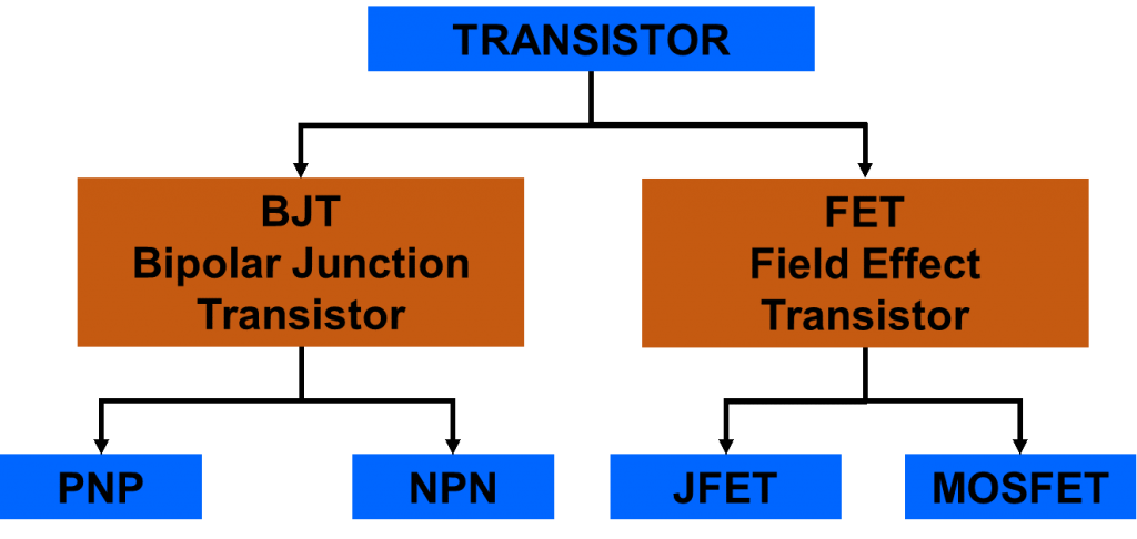
There are two types of standard bipolar transistors, namely PNP & NPN transistors. In this article, one of them, namely PNP, will be discussed in detail.
- Definition of PNP Transistor
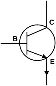
- PNP Transistor Symbol
- Diagram
- Configuration
- Working Principle
- Applications
- Advantages-Disadvantages
- PNP Transistor as a Switch
- PNP vs NPN Transistor
PNP Transistor Definition
“A P-N-P Transistor is a BJT type built by merging an N-type semiconductor between two P-type semiconductors.”
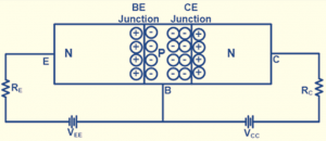
PNP Transistor Diagram:
The transistor consists of three section-
- E-Emitter
- B-Base
- C-Collector
On the subject of the working of three terminals of the PNP transistor,
- The emitter is used to provide charge carriers into the collector through the Base area.
- The Collector region gathers most of the charge carriers emitted in the emitter.
- The base used to controls the quantity of current pass through the Emitter to Collector.
PNP Transistor Symbol

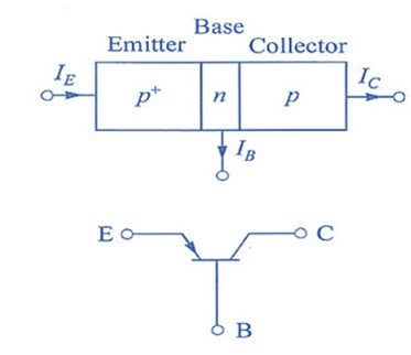
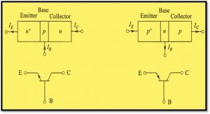
The mid-layer (N-type) is termed as the B- Base terminal. The left-sided P-type layer works as an E- Emitter terminal and the right-sided P-type layer known as a C-Collector terminal.
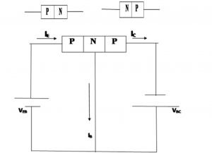
In an N-P-N transistor formation, One P-type semiconductor material is fit in between two N-type semiconductors, as explained in the article (Link NPN transistor). Whereas in a P-N-P transistor, one N-type semiconductor is fit in between two P-type semiconductors material.
In a PNP transistor, two types of diodes are used. They are respectively P-N and N-P diode. These P-N junction diodes are called the collector-base or C-B junction and base-emitter or B-E junction.
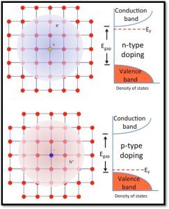
In the P-type semiconductor material, the charge carriers are holes primarily. So, in this transistor, the current formation is due to the movement of holes only.
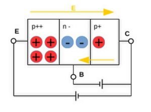
The (P-type) Emitter and Collector regions are comparatively doped more than the N-type Base. The regions of the Emitter and Collector regions are wider in comparison to the base.
An adequately more number of free electrons are available in an N-type semiconductor, usually. But, the width of the mid-layer is narrower and lightly doped in this case.
PNP Transistor Working Principle
The Emitter-Base intersection is linked to forwarding bias. Along with also the +ve terminal of a voltage supply (VCB) is connected with all the Base terminal (N-type), and the -ve terminal is linked with all the Collector terminal (P-type). Consequently, the Collector-Base intersection is associated with reverse biasing.
As a result of this biasing, the depletion area at the E-B junction is less since it’s linked to forwarding bias. Even though the C-B junction is in reverse bias, the depletion area at the Collector-Base junction is wide enough. The E-B junction is forward biased. Therefore, more hole moves from emitters across the depletion area and acts as an input to the base. Simultaneously, not many electrons carried in an emitter in the base and recombined with the holes.
But the amount of electrons at the base is minimal since it’s a reasonably less doped and narrow area. Therefore, almost all Emitter regions’ holes will pass the depletion region and carried into the Base regions.
The current will pass through the E-B junction. This is Emitter current (IE). So IC, the Collector current will pass through the Collector-Base layers because of holes.

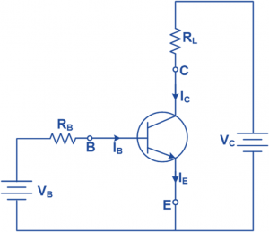
PNP Transistor Circuit
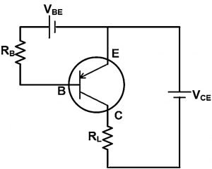
When a PNP transistor is linked with voltage resources, the base current will be carried in the transistor. Even the little quantity of base present controls the circulation of a massive number of current through the emitter to collector supplied the Base voltage is more -ve compared to Emitter voltage.
When VB the base voltage isn’t -ve in comparison to the VE the emitter voltage, the current can’t pass within the circuit. So, it’s necessary to provide a voltage supply in reverse bias > 0.72 Volt.
The resistors RL and RB are connected in the circuit. That to restricts the current to pass through the transistor’s maximum possible height.
The Emitter’s voltage is VEB as input side. Here the emitter current (IE) flows from the input side, and it flows in two directions; one is IB and other is IC.
IE= IB+ IC
But only 2 to 5 % of the total current flows in the IB, so IB is negligible.
Advantages of PNP Transistor
- Small in size and could be utilized as a part of IC design.
- Comparatively cheap, long-lasting and simpler circuit.
- Spontaneous actions available
- Low supply voltage requirement and less output impedance.
- Produce less noise than NPN Transistors.
Disadvantages of PNP Transistor
- Not suitable to operate on high-frequency application.
- Perform slowly in comparison to NPN.
- Temperature sensitivity and may get damaged during a thermal runaway.
PNP transistors Applications:
- PNP transistors are applied as switches, i.e., analog switches, emergency push button etc. They have applications when emergency shutdown required.
- These types of transistors are used in current sources circuitry, i.e., by exploiting the characteristics of current flows out of the collector.
- It’s applied in the amplifying circuits.
- They are used in Darlington pair circuits.
- The P-N-P type transistors are used in heavy motors to control current flow and various robotic and microcontroller design applications.
PNP Transistor as a Switch
Once the switch is ON, the current will pass through the circuit and also behave as a close circuit. The transistor is an analogue power electronics-based circuitry with changeover characteristics which may function like ordinary switches.
As we have observed in the P-N-P transistor’s working, When the Base voltage isn’t more –ve than the VE, the current will not able to pass through the circuit. Thus, VB is at least 0.72 Volt in reverse bias connection to operate the transistor.
So, if the VB is 0 or > 0.72Volt, the current will not pass and operate as an open switch.
PNP vs NPN Transistor
| PNP Transistor | NPN Transistor |
| PNP stands for Positive-Negative-Positive transistors | An NPN Transistor stands for Negative-Positive-Negative transistor. |
| A PNP transistor needs negative current flow from the base to emitter. | An NPN transistor needs positive current flow from the base to emitter. |
| A PNP transistor gets positive voltage at the emitter terminal. This +ve voltage permits the current emitter to collector. | An NPN transistor gets +ve voltage in the collector terminal. This +ve allows the current to flow from collector to emitter. |
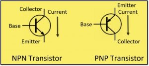
In the case of PNP transistor, the current directed from the emitter to base. Once the transistor is switched ON, current pass through the emitter to collector. When current is supplied from the transistor base to emitter in an NPN transistor, the transistor base gets a positive voltage, and the emitter receives a negative voltage. Thus the current flows into the base. When there is enough current flowing from base into the emitter, the transistor is switched ON, and it directs the current flow from the collector to emitter instead of base to emitter.
To know more about electronics click here
