33 QA:Modulation Index,Multiplexing,Modulation & Demodulation

AM Signal 300x190 1

Modulation and demodulation are fundamental concepts in communication systems that play a crucial role in transmitting and receiving information. In this section, we will explore the definitions of modulation and demodulation, as well as the importance of these processes in communication systems.

Definition of Modulation

Modulation is the process of modifying a carrier signal to encode information. In simpler terms, it involves altering certain characteristics of the carrier signal, such as amplitude, frequency, or phase, in order to carry the desired information. By modulating the carrier signal, we can efficiently transmit information over long distances and through various media.

Definition of Demodulation

AM Signal
AlmuhammediArabic WikipediaAmplitude ModulationWikimedia Commons

Demodulation, also known as detection or extraction, is the reverse process of modulation. It involves extracting the original information from the modulated carrier signal. Demodulation is necessary at the receiving end to recover the transmitted information accurately. By demodulating the received signal, we can retrieve the original data and make it usable for further processing or interpretation.

Importance of Modulation and Demodulation in Communication Systems

Modulation and demodulation are vital components of communication systems for several reasons. Let’s explore some of their key importance:

  1. Efficient Transmission: Modulation allows us to transmit information efficiently over different types of communication channels. By modifying the carrier signal, we can adapt it to the specific characteristics of the transmission medium, such as bandwidth limitations or noise interference. This enables us to achieve better signal quality and maximize the utilization of available resources.

  2. Compatibility: Modulation techniques enable compatibility between different communication systems. By using standardized modulation schemes, such as amplitude modulation (AM), frequency modulation (FM), or phase modulation (PM), we can ensure that different devices and systems can communicate with each other effectively. This compatibility is crucial in enabling seamless communication across various platforms and technologies.

  3. Signal Integrity: Modulation helps in preserving the integrity of the transmitted signal. By modulating the carrier signal, we can make it less susceptible to noise, interference, and distortion during transmission. This ensures that the received signal retains its quality and fidelity, allowing for accurate demodulation and extraction of the original information.

  4. Multiplexing: Modulation techniques enable the transmission of multiple signals simultaneously over a single communication channel. This is achieved through techniques like frequency division multiplexing (FDM) or time division multiplexing (TDM). By modulating each signal with a unique carrier frequency or time slot, multiple signals can be combined and transmitted together, significantly increasing the efficiency and capacity of the communication system.

Modulation Index

The modulation index is a crucial parameter in the field of communication systems, particularly in the context of modulation and demodulation techniques. It plays a significant role in determining the quality and efficiency of the transmitted signal. In this section, we will explore the definition of modulation index, its explanation in amplitude modulation (AM), the calculation of modulation index, and the effects it has on the transmitted signal.

Definition of Modulation Index

The modulation index, also known as the modulation depth, is a dimensionless quantity that represents the extent of modulation in a communication system. It quantifies the relationship between the amplitude of the modulating signal and the amplitude of the carrier signal. Essentially, it indicates how much the carrier signal is being varied or modulated by the information-bearing signal.

Explanation of Modulation Index in Amplitude Modulation (AM)

In amplitude modulation (AM), the modulation index determines the variation in the amplitude of the carrier signal. It is defined as the ratio of the peak amplitude of the modulating signal to the peak amplitude of the carrier signal. A higher modulation index signifies a greater variation in the amplitude of the carrier signal, resulting in a more significant modulation effect.

When the modulation index is low, the amplitude of the carrier signal remains relatively constant, and the modulating signal has minimal impact on the transmitted signal. On the other hand, a high modulation index leads to a more pronounced variation in the amplitude of the carrier signal, allowing the modulating signal to have a more significant influence on the transmitted signal.

Calculation of Modulation Index

The modulation index can be calculated using the formula:

Modulation Index = (Amplitude of Modulating Signal) / (Amplitude of Carrier Signal)

For example, if the amplitude of the modulating signal is 5 volts and the amplitude of the carrier signal is 10 volts, the modulation index would be 0.5. This indicates that the modulating signal is half the amplitude of the carrier signal.

Effects of Modulation Index on the Transmitted Signal

The modulation index has a direct impact on the characteristics of the transmitted signal. It influences the bandwidth, power efficiency, and quality of the signal. Let’s explore the effects of different modulation index values:

  1. Low Modulation Index: When the modulation index is low (close to zero), the transmitted signal is primarily composed of the carrier signal. The modulating signal has minimal effect on the signal, resulting in a narrow bandwidth. However, the information carried by the modulating signal may be difficult to discern due to the low level of modulation.

  2. Moderate Modulation Index: A moderate modulation index value (between 0.5 and 1) allows for a more significant variation in the amplitude of the carrier signal. This results in a wider bandwidth and improved signal quality. The information carried by the modulating signal is more easily distinguishable.

  3. High Modulation Index: When the modulation index is high (greater than 1), the transmitted signal experiences a substantial variation in amplitude. This leads to an even wider bandwidth and a higher level of modulation. However, excessive modulation can cause distortion and signal degradation, affecting the quality of the transmitted signal.

Phase Modulation

Phase modulation is a modulation technique used in communication systems to transmit information by varying the phase of a carrier wave. It is closely related to frequency modulation (FM) and amplitude modulation (AM), but instead of varying the frequency or amplitude, phase modulation focuses on changing the phase of the carrier wave.

Definition of Phase Modulation

In phase modulation, the phase of the carrier wave is modified in accordance with the input signal. The input signal, also known as the modulating signal, contains the information to be transmitted. By altering the phase of the carrier wave, the modulating signal is effectively encoded onto the carrier wave.

Phase modulation can be mathematically represented as:

s(t) = A * cos(wc * t + β * m(t))

Where:
s(t) is the modulated signal
A is the amplitude of the carrier wave
wc is the angular frequency of the carrier wave
t is the time
β is the modulation index
m(t) is the modulating signal

Comparison of Phase Modulation with Other Modulation Techniques

Phase modulation shares similarities with frequency modulation (FM) and amplitude modulation (AM), but it also has distinct characteristics that set it apart.

Frequency Modulation (FM)

In FM, the frequency of the carrier wave is varied in proportion to the modulating signal. This means that the frequency deviation is directly related to the amplitude of the modulating signal. In contrast, phase modulation focuses on altering the phase of the carrier wave, which is not directly dependent on the amplitude of the modulating signal.

Amplitude Modulation (AM)

AM involves varying the amplitude of the carrier wave in response to the modulating signal. This modulation technique is commonly used in broadcasting, where the amplitude variations carry the audio signal. Phase modulation, on the other hand, does not directly manipulate the amplitude of the carrier wave. Instead, it encodes information by modifying the phase.

Advantages and Disadvantages of Phase Modulation

Like any modulation technique, phase modulation has its own set of advantages and disadvantages.

Advantages

  1. Robustness: Phase modulation is less susceptible to noise and interference compared to amplitude modulation. This makes it a reliable choice for transmitting signals in noisy environments.

  2. Bandwidth Efficiency: Phase modulation offers better bandwidth efficiency compared to amplitude modulation. It allows for the transmission of more information within the same frequency range.

  3. Improved Signal Quality: Phase modulation provides improved signal quality, as it is less affected by variations in amplitude. This results in clearer and more reliable communication.

Disadvantages

  1. Complexity: Phase modulation requires more complex circuitry and processing compared to amplitude modulation. This can increase the cost and complexity of the communication system.

  2. Limited Range: Phase modulation is more sensitive to changes in the carrier wave’s phase. This can limit the range of the transmitted signal, especially in scenarios with high levels of interference.

Effects of Modulation Index on AM Waves

The modulation index plays a crucial role in determining the characteristics of amplitude modulation (AM) waves. It is a measure of how much the amplitude of the carrier wave is varied in response to the modulating signal. In this section, we will explore how the modulation index affects AM waves and the implications of doubling the modulation index.

Explanation of how the modulation index affects AM waves

The modulation index, also known as the modulation depth or modulation factor, is defined as the ratio of the peak amplitude of the modulating signal to the peak amplitude of the carrier wave. It quantifies the extent to which the modulating signal influences the amplitude of the carrier wave.

When the modulation index is low, the amplitude variations in the carrier wave are minimal. This results in a narrow bandwidth and a lower quality of the modulated signal. On the other hand, a high modulation index leads to significant amplitude variations in the carrier wave, resulting in a wider bandwidth and a higher quality of the modulated signal.

To better understand the effects of the modulation index, let’s consider an example. Suppose we have a carrier wave with a peak amplitude of 10 volts and a modulating signal with a peak amplitude of 5 volts. If the modulation index is 0.5, the amplitude of the carrier wave will vary between 7.5 volts and 12.5 volts. As the modulation index increases, the amplitude variations become more pronounced, resulting in a more pronounced modulation of the carrier wave.

Doubling the modulation index of an AM wave

Doubling the modulation index of an AM wave has significant implications for the modulated signal. When the modulation index is doubled, the amplitude variations in the carrier wave become more pronounced. This leads to an increase in the bandwidth of the modulated signal.

A wider bandwidth allows for the transmission of more information, as it accommodates a greater range of frequencies. However, it also requires more resources in terms of transmission power and bandwidth allocation. Therefore, doubling the modulation index should be done with caution, considering the trade-off between increased information transmission and resource utilization.

In addition to the bandwidth implications, doubling the modulation index can also affect the demodulation process. The demodulator, which extracts the original modulating signal from the modulated carrier wave, relies on the modulation index to accurately recover the modulating signal. If the modulation index is too low, the demodulator may struggle to extract the modulating signal accurately. Conversely, if the modulation index is too high, the demodulator may introduce distortion or inaccuracies in the recovered signal.

Why Modulation Index is Less Than 1

In most modulation techniques, the modulation index is typically less than 1. This value plays a crucial role in determining the quality and efficiency of the modulation process. Let’s explore the reasons behind this phenomenon, the relationship between modulation index and signal quality, and the impact it has on the efficiency of modulation.

Reasons for Modulation Index Being Less Than 1 in Most Modulation Techniques

MCQ on Electronics

There are several reasons why the modulation index is generally kept below 1 in most modulation techniques:

  1. Avoiding Overmodulation: Overmodulation occurs when the modulation index exceeds 1. This can lead to distortion and interference in the transmitted signal. By keeping the modulation index below 1, we ensure that the signal remains within the acceptable range and avoids overmodulation.

  2. Preventing Signal Interference: When the modulation index is less than 1, the sidebands produced during modulation are spaced closer together. This reduces the chances of interference with neighboring channels or frequencies, allowing for efficient use of the available bandwidth.

  3. Minimizing Power Consumption: In many modulation techniques, the power required to transmit a signal increases as the modulation index approaches 1. By keeping the modulation index below 1, we can minimize power consumption while still achieving satisfactory signal quality.

Relationship Between Modulation Index and Signal Quality

The modulation index has a direct impact on the quality of the modulated signal. Here’s how it affects signal quality:

  1. Signal Fidelity: The modulation index determines the extent to which the original message signal can be accurately reproduced at the receiver. A higher modulation index allows for better fidelity, as it provides a wider range of amplitudes to represent the message signal. However, if the modulation index is too high, it can lead to distortion and signal degradation.

  2. Signal-to-Noise Ratio (SNR): The modulation index affects the SNR of the modulated signal. A higher modulation index generally results in a higher SNR, as it allows for a larger portion of the transmitted power to be allocated to the signal. This leads to improved signal quality and better reception.

  3. Bandwidth Efficiency: The modulation index also influences the bandwidth efficiency of the modulation technique. By keeping the modulation index below 1, we can ensure that the sidebands are closely spaced, allowing for efficient use of the available bandwidth. This is particularly important in applications where bandwidth is limited or expensive.

Impact of Modulation Index on the Efficiency of the Modulation Process

The modulation index plays a crucial role in determining the efficiency of the modulation process. Here’s how it impacts efficiency:

  1. Power Efficiency: By keeping the modulation index below 1, we can achieve a balance between signal quality and power consumption. Higher modulation indices require more power to transmit the same signal, leading to decreased power efficiency. By optimizing the modulation index, we can maximize power efficiency without compromising signal quality.

  2. Spectral Efficiency: Spectral efficiency refers to the amount of information that can be transmitted per unit of bandwidth. By keeping the modulation index below 1, we can achieve higher spectral efficiency by closely packing the sidebands within the available bandwidth. This allows for more efficient use of the frequency spectrum.

MCQs on Modulation and Demodulation

MCQs related to modulation index

  1. What is the modulation index?
  2. The modulation index is a parameter that determines the extent of modulation in a signal.
  3. It is defined as the ratio of the peak amplitude of the modulating signal to the peak amplitude of the carrier signal.
  4. A higher modulation index indicates a higher degree of modulation.

  5. What is the significance of the modulation index?

  6. The modulation index determines the bandwidth occupied by the modulated signal.
  7. It affects the quality of the demodulated signal and the efficiency of the modulation technique.
  8. A modulation index of 1 is considered optimal for most modulation schemes.

  9. How does the modulation index affect the bandwidth?

  10. The bandwidth of a modulated signal is directly proportional to the modulation index.
  11. A higher modulation index leads to a wider bandwidth.
  12. This is because a higher modulation index introduces more sidebands around the carrier frequency.

MCQs related to modulation and demodulation techniques

  1. What is Amplitude Modulation (AM)?
  2. AM is a modulation technique where the amplitude of the carrier signal varies in accordance with the modulating signal.
  3. It is commonly used in broadcasting and two-way communication systems.
  4. AM signals can be demodulated using envelope detection or synchronous detection techniques.

  5. What is Frequency Modulation (FM)?

  6. FM is a modulation technique where the frequency of the carrier signal varies with the modulating signal.
  7. It is widely used in FM radio broadcasting and high-fidelity audio transmission.
  8. FM signals can be demodulated using frequency discriminators or phase-locked loop (PLL) circuits.

  9. What is Phase Modulation (PM)?

  10. PM is a modulation technique where the phase of the carrier signal is varied in accordance with the modulating signal.
  11. It is commonly used in digital communication systems and satellite communication.
  12. PM signals can be demodulated using phase detectors or Costas loop circuits.

MCQs on the working principles of modulation and demodulation

  1. How does modulation work?
  2. Modulation involves combining a low-frequency information signal (modulating signal) with a high-frequency carrier signal.
  3. The modulating signal alters the characteristics of the carrier signal, such as amplitude, frequency, or phase.
  4. This modulated signal is then transmitted through a communication channel.

  5. How does demodulation work?

  6. Demodulation is the process of extracting the original modulating signal from the modulated carrier signal.
  7. The demodulator circuit or receiver reverses the modulation process to recover the original signal.
  8. The demodulation technique used depends on the modulation scheme employed.

  9. What are the advantages of modulation and demodulation?

  10. Modulation allows multiple signals to be transmitted simultaneously over a shared medium.
  11. It enables long-distance communication and reduces interference between different signals.
  12. Demodulation allows the receiver to extract the original information signal accurately.

How Modulation and Demodulation Work

Modulation and demodulation are fundamental processes in communication systems that allow the transmission and reception of information over long distances. These processes involve the manipulation of a carrier signal to carry the desired information. Let’s explore how modulation and demodulation work in more detail.

Explanation of the Process of Modulation

Modulation is the process of modifying a high-frequency carrier signal with the information to be transmitted. The carrier signal acts as a “vehicle” for the information, allowing it to be efficiently transmitted over long distances. There are several types of modulation techniques, including amplitude modulation (AM), frequency modulation (FM), and phase modulation (PM).

In amplitude modulation, the amplitude of the carrier signal is varied in proportion to the instantaneous amplitude of the modulating signal. This variation in amplitude represents the information being transmitted. For example, in AM radio broadcasting, the audio signal is used to modulate the amplitude of the carrier signal, allowing the transmission of voice or music.

Frequency modulation, on the other hand, involves varying the frequency of the carrier signal based on the instantaneous amplitude of the modulating signal. This variation in frequency represents the information being transmitted. FM is commonly used in radio broadcasting, where the frequency of the carrier signal is modulated to carry audio signals.

Phase modulation, as the name suggests, involves varying the phase of the carrier signal based on the instantaneous amplitude of the modulating signal. This variation in phase represents the information being transmitted. Phase modulation is widely used in digital communication systems, such as satellite communication and wireless networks.

Explanation of the Process of Demodulation

Demodulation, also known as detection or extraction, is the process of recovering the original information from the modulated carrier signal. It is the reverse process of modulation and is essential for receiving and decoding the transmitted signal accurately.

Demodulation involves extracting the original information from the modulated carrier signal by using a demodulator or detector circuit. The demodulator circuit is designed to detect and separate the modulating signal from the carrier signal. The demodulator circuit can be specifically designed based on the modulation technique used.

For example, in AM demodulation, a diode detector circuit can be used to rectify the modulated signal, resulting in the recovery of the original audio signal. In FM demodulation, a frequency discriminator or phase-locked loop (PLL) circuit can be employed to detect the frequency variations and recover the original modulating signal.

Overview of the Components Involved in Modulation and Demodulation

Modulation and demodulation involve several components that work together to ensure the accurate transmission and reception of information. These components include:

  1. Carrier Signal: The high-frequency signal that is modulated to carry the information.

  2. Modulating Signal: The information signal that is used to modulate the carrier signal. This can be an audio signal, video signal, or data signal.

  3. Modulator: The circuit or device that performs the modulation process. It combines the carrier signal and the modulating signal to produce the modulated signal.

  4. Demodulator: The circuit or device that performs the demodulation process. It separates the modulating signal from the modulated carrier signal, allowing the recovery of the original information.

  5. Transmission Medium: The physical medium through which the modulated signal is transmitted. This can be a wired medium, such as coaxial cables or optical fibers, or a wireless medium, such as radio waves or microwaves.

By understanding the process of modulation and demodulation, we can appreciate how information is efficiently transmitted and received in various communication systems. These processes form the backbone of modern telecommunications, enabling us to communicate and exchange information over vast distances.

Modulation Index Calculation

The modulation index is a crucial parameter in modulation and demodulation techniques. It quantifies the extent of modulation applied to a carrier signal. By calculating the modulation index, we can determine the efficiency and quality of the modulation process. In this section, we will explore the step-by-step guide to calculating the modulation index and provide examples for different modulation techniques.

Step-by-step guide to calculating modulation index

To calculate the modulation index, we need to consider the peak amplitude of the modulating signal and the peak amplitude of the carrier signal. The formula for calculating the modulation index varies depending on the modulation technique used. Here is a step-by-step guide to calculating the modulation index for different modulation techniques:

  1. Amplitude Modulation (AM): In AM, the modulation index represents the ratio of the peak amplitude of the modulating signal to the peak amplitude of the carrier signal. The formula for calculating the modulation index in AM is as follows:

Modulation Index (m) = (Amplitude of Modulating Signal) / (Amplitude of Carrier Signal)

For example, if the peak amplitude of the modulating signal is 10 volts and the peak amplitude of the carrier signal is 5 volts, the modulation index would be:

m = 10 V / 5 V = 2

  1. Frequency Modulation (FM): In FM, the modulation index is determined by the ratio of the frequency deviation to the modulating frequency. The formula for calculating the modulation index in FM is as follows:

Modulation Index (m) = (Frequency Deviation) / (Modulating Frequency)

For instance, if the frequency deviation is 50 kHz and the modulating frequency is 10 kHz, the modulation index would be:

m = 50 kHz / 10 kHz = 5

  1. Phase Modulation (PM): In PM, the modulation index is calculated by dividing the phase deviation by the modulating frequency. The formula for calculating the modulation index in PM is as follows:

Modulation Index (m) = (Phase Deviation) / (Modulating Frequency)

For example, if the phase deviation is 30 degrees and the modulating frequency is 1 kHz, the modulation index would be:

m = 30 degrees / 1 kHz = 30 degrees/kHz

Examples of modulation index calculations for different modulation techniques

Let’s consider a few examples to illustrate the calculation of the modulation index for different modulation techniques:

  1. Example 1: AM Modulation

  2. Amplitude of Modulating Signal: 8 V

  3. Amplitude of Carrier Signal: 4 V

Modulation Index (m) = 8 V / 4 V = 2

Therefore, the modulation index for this AM modulation example is 2.

  1. Example 2: FM Modulation

  2. Frequency Deviation: 25 kHz

  3. Modulating Frequency: 5 kHz

Modulation Index (m) = 25 kHz / 5 kHz = 5

Hence, the modulation index for this FM modulation example is 5.

  1. Example 3: PM Modulation

  2. Phase Deviation: 45 degrees

  3. Modulating Frequency: 2 kHz

Modulation Index (m) = 45 degrees / 2 kHz = 45 degrees/kHz

Thus, the modulation index for this PM modulation example is 45 degrees/kHz.

Frequently Asked Questions

1. What is modulation index in phase modulation?

The modulation index in phase modulation refers to the ratio of the maximum phase deviation to the frequency deviation of the carrier signal.

2. What happens when the modulation index of an AM wave is doubled?

When the modulation index of an AM wave is doubled, the amplitude of the sidebands also doubles, resulting in an increase in the bandwidth of the modulated signal.

3. Why is the modulation index less than 1?

The modulation index is typically less than 1 to ensure that the modulation does not cause distortion or overmodulation of the carrier signal. It helps maintain the integrity of the transmitted signal.

4. Are there any MCQs available on modulation index?

Yes, there are multiple-choice questions (MCQs) available on modulation index that can help test your understanding of this concept.

5. Where can I find MCQs on modulation and demodulation?

You can find MCQs on modulation and demodulation in various textbooks, online learning platforms, or educational websites that cover the topic of communication systems.

6. How does modulation and demodulation work?

Modulation is the process of superimposing information signals onto a carrier signal, while demodulation is the process of extracting the original information signals from the modulated carrier signal. This is achieved using modulation and demodulation techniques such as amplitude modulation (AM), frequency modulation (FM), or phase modulation (PM).

7. What does the modulation index indicate?

The modulation index indicates the extent of modulation applied to a carrier signal. It determines the amplitude, frequency, or phase variations of the carrier signal based on the information signal.

8. How is modulation achieved?

Modulation is achieved by varying one or more characteristics of a carrier signal, such as amplitude, frequency, or phase, in accordance with the information signal. This variation allows the information to be transmitted over a communication channel.

9. What happens to the transmitted power when the modulation index of an AM wave is increased from 0.5 to 1?

When the modulation index of an AM wave is increased from 0.5 to 1, the transmitted power remains constant. However, the power distribution between the carrier and the sidebands changes, with the sidebands gaining more power.

10. How is modulation index calculated?

The modulation index can be calculated by dividing the peak amplitude of the modulating signal by the peak amplitude of the carrier signal. It represents the extent of modulation applied to the carrier signal.

35 Important MCQ On Microprocessors And Microcontrollers

1. The fetch and execute instruction, one at a time, in the order of address increment is identified as

  1. The Instruction execution technique
  2. The Straight line sequencing technique
  3. The Instruction fetching technique
  4. The Random sequencing technique

Answer – (2)

2. The control signal employed to differentiate amongst an input  or output operation and memory operations is

  1. ALE
  2. IO/ M͞
  3. SID
  4. SOD

Answer – (2)

3. The instruction register hold

  1. The Flag condition
  2. An Instruction address
  3. An Opcode
  4. None

Answer – (3)

4. A microprocessor is termed to be a 8-bit or 16-bit or more considering the

  1. Size of data bus
  2. Size of Address bus
  3. Size of Arithmetic Logic Unit
  4. Size of Control bus

Answer – (3)

5. The number of pair register  found in 8085 microprocessor

  1. Three
  2. Four
  3. two
  4. Zero

Answer – (1)

6. The number of programmable 8-bit registers of microprocessor 8085 is

  1. five
  2. Six
  3. Seven
  4. Eight

Answer – (3)

7. The stack and SP in microprocessor

  1. Belong to the memory
  2. Both reside in CPU
  3. Both reside in memory and later in CPU
  4. Former reside in CPU and the later in memory

Answer – (3)

8. An 8kX8 ROM, having the monitor program of microprocessor trainer-kit with end-address of

  1. 600FH
  2. 500FH
  3. 1 FFF H
  4. 4 FFF H

Answer – (3)

9. The overall I/O space existing in a 8085 if used as a peripheral mapped mode

  1. Sixty four only
  2. One hundred twenty eight
  3. Two hundred fifty six
  4. Five hundred twelve

Answer – (3)

10. The interfacing device utilized with an O/P port be there

  1. Buffer circuit
  2. Priority encoder circuit
  3. Latch circuit
  4. None

Answer – (1)

11. Address lines necessitate for the 64kB memory is

  1. 24
  2. 36
  3. 12
  4. 16

Answer – (4)

12. Which one is hardware type interrupt?

  1. INTA
  2. TRAP
  3. RST
  4. INT

Answer – (2)

13. In 8085 microprocessor, which one is the non-maskable interrupt?

  1. RST 7.5
  2. TRAP
  3. HOLD
  4. INTR

Answer – (2)

14. Machine cycles in the “CALL” instruction of microprocessor 8085 CPU are

  1. six
  2. five
  3. four
  4. two

Answer – (2)

15. In 8085 Microprocessor, the interrupt TRAP is

  1. Every time maskable
  2. not interrupted  by a service subroutine
  3. Used for short-term power failure
  4. Lowermost priority interrupt

Answer – (3)

16. RST 7.5 interrupt act as

  1. Vectored and Maskable type
  2. Vectored and non-maskable type
  3. Direct and maskable type
  4. Direct and non-maskable type

Answer – (1)

17. No of hardware interrupt request, a solitary interrupt- controller  namely IC8259A could process?

  1. Eight
  2. Nine
  3. Sixteen
  4. Sixty four

Answer – (1)

18. The interrupt mask in the 8085 microprocessor is set or reset by the software instruction

  1. By the EI interrupt
  2. By the DI interrupt
  3. By the RIM interrupt
  4. By the SIM interrupt

Answer – (4)

19. For 8085, The vector address corresponding to software interrupt RST 7.0 is

  1. 0017 Hex
  2. 0027 Hex
  3. 0038 Hex
  4. 0700 Hex

Answer – (3)

20. Which one has the highest priority out of these

  1. TRAP
  2. RST 7.5
  3. RST 6.5
  4. HOLD

Answer – (4)

21. Which one of the following is the software interrupt of 8085 ?

  1. RST 7.5
  2. EI
  3. RST 1.0
  4. TRAP

Answer – (3)

22. Let the accumulator content 4F after execution the RAL instruction, contain of accumulator will be

  1. 9E
  2. 8B
  3. 8C

Answer – (1)

23. The clock’s interrupt-handler of a certain computational machine needs 2 m/sec per clock tick. The clock’s frequency is 60 Hz. What percent of the CPU is dedicated to the clk?

  1. 1.2
  2. 7.5
  3. 12
  4. 18.5

Answer – (3)

24. For “JZ NEXT” instruction, which of the following register’s memory is checked to verify if it is ‘0’ or not ?

  1. A
  2. B
  3. R1
  4. R2

Answer – (1)

25. At any time POP H instruction is performed

  1. Data bytes in the HL pairs will be put in storage of the stack’s registers
  2. Two data bytes are transferred to the HL pair’s register
  3. Two data bytes at the top of the stack are moved to the CPU

Answer – (2)

26. In microprocessor instruction STA 9000H is  

  1. A data transfer instruction
  2. A Logical instruction
  3. A I/O and MPU will execute
  4. Not an option

Answer – (1)

27. The addressing method in microprocessor used in the STAX B is

  1. A Direct addressing method
  2. A Resister addressing  method
  3. An Immediate addressing method
  4. Register indirect addressing method

Answer – (4)

28. When a subroutine is called the address of the instruction next to CALL is kept in

  1. The Stack
  2. The Program counter
  3. The Stack pointer register
  4. Not an option

Answer – (1)

29. Machine cycles for IN instructions in microprocessor are

  1. Eight
  2. five
  3. four
  4. three

Answer – (4)

 30. The instruction MOV A, B is kind of

  1. the Immediate addressing mode
  2. Directing addressing mode
  3. Implied addressing mode
  4. Register addressing mode

Answer – (4)

31. How many T-states would be required for the execution of CALL 2000 H instruction?

  1. 10
  2. 13
  3. 18
  4. None of these

Answer – (3)

32. The number of I/O lines for 8255 chip is

  1. 256
  2. 512
  3. 1024
  4. 2K

Answer – (1)

33. How many flag registers are available in the 8051 chip?

  1. 9
  2. 8
  3. 6
  4. 5
  5. None

Answer – (5)

34. The “programmable interval timer” is

  1. 8253 chip
  2. 8251 chip
  3. 8250 chip
  4. 8275 chip

Answer – (1)

35. The 8086 microprocessor addressing capacity is

  1. 64 KB
  2. 1 MB
  3. 2 MB
  4. 1 GB

Answer – (2)

To Learn more on Electronics click here

8086 Microprocessor: 7 Interesting Facts To Know

8086 1 300x202 1

CONTENTS

  • Intel 8086
  • PIN diagram
  • Different addressing modes
  • Different Flags Register
  • Pipeline architecture in 8086 microprocessor
  • Advantage of pipelining
  • Memory segmentation in 8086
  • Difference between 8085 and 8086 microprocessor

What is Microprocessor 8086?

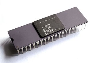
8086 1
8086 microprocessor
Image Credit :Thomas NguyenIntel C8086CC BY-SA 4.0

INTEL 8086:

  • Microprocessor 8086 first invented by INTEL in 1976.
  • 8086 is equipped with 16-bit, HMOS N-channel based microprocessor.
  • This has two modes; minimum and maximum.
  • 8086 has total twenty (20) address lines
  • 8086 has sixteen (16) data lines.

PIN diagram of 8086 microprocessor:

8086 Microprocessor
8086 Microprocessor. Image Credit; Unknown authorUnknown author, Wyprowadzenie mikroprocesora 8086, marked as public domain, more details on Wikimedia Commons

What is Addressing Mode?

“Addressing mode is the way to specify a particular data to be operated by an instruction.”

We need different types of addressing mode because it provides flexibility to the programmer to access data.

What are the types of Addressing Mode in 8086?

The different types of Addressing Modes are explained below:

Register Addressing: 

The operand is a register.

                                     Example – MOV, AX, BX

Immediate Addressing:

The instruction itself comprises the operands.

                                     Example – MOV, AX, 5000H

Direct Addressing:

The instruction specifies the address the operand.

                                    Example – MOV, AX, 9000H

Indexed Addressing:

The operand is specified using one of SI and DI as index register, along with an optional offset. The address of operand is acquired by addition of the information of the index register with the offset, if present.

                                      Example – MOV AX, [SI] or MOV AX, [SI+1000H]

Based Addressing:

The operand is specified using one of BX and BP as base register, along with an optional offset. The address of operand is acquired by addition of the information of base register with the offset, if present.

                                     Example – MOV AX, [BX] or MOV AX, [BP+1000H]

Based-Indexed Addressing:

The operand is specified using one of SI and DI as index register and ones of BX and BP as base register, along with an optional offset. The address of the operand is acquired by addition of information of the index register with the contents of the base register and the offset, if present.

                                    Example – MOV AX, [SI+BX] or MOV AX, [DI+BP+1000H]

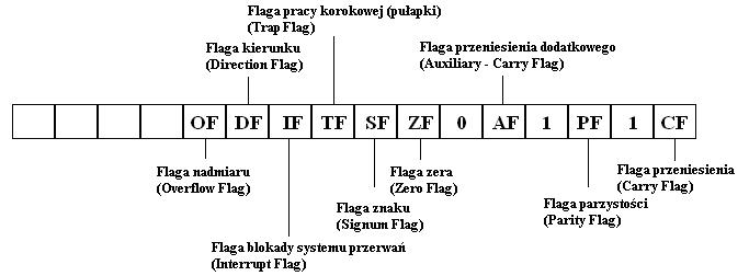
Different Flags in 8086 Microprocessor:

  1. S (Sign Flag) – Set when answer of computation is negative.
  2. Z (Zero) – Set when computation of previous instruction is zero.
  3. P (Parity) – Set when lower byte contains even number of ones.
  4. C (Carry) – When there have carry in computation.
  5. T (Trap) – when processor enters single step instruction mode.
  6. I (Interrupt) – Maskable interrupts are identified.
  7. D (Direction) – In string manipulation.
  8. AC (Auxiliary Carry)
  9. O (Overflow) – When result is larger to accommodate in registers.
Rejestr flag 8086
Register Flag

Pipeline Architecture in 8086 Microprocessor:

The fundamental idea of pipelined architecture is to sub divide the processing of a computer instructions into a series of independent stage (like “pre-fetch”, “fetch”, “decode”, “execute” etc.) with storage at the end of each step.

This permits the computer’s control to instruct the processing speed of the slowest step that is a lot quicker than the time requirement to do all steps at the same time. The pipeline signifies how every step is taking information simultaneously, and any step is linked to subsequent one.

In this, there are 2 separate units

– The “Bus Interface Unit” (BIU)

–  The “Execution Unit” (EU).

The BIU executes all bus operations for the execution unit. The data is in communication in between the CPU and memories and input output kit upon request from the EU. During this if the EU is active implementing commands, the BIU “look ahead” and brings more instruction from the memory. This way, a type of “Fetch-Execute-Pipeline” is implemented in 8086.

Write down some of the Advantages and Disadvantages of Pipelining?

The advantages of pipelining are:

• The cycle time of the chip is comparatively lesser. Pipelining does not minimize the time necessary to finish an instruction; rather it raises the quantity of instructions which may be processed concurrently and reduces the delay between complete instructions.

• The multiple no increased pipeline stages means that more commands could be processed at once and the less delay in between the commands. Every overriding simulated microprocessor manufactured today uses at least two stage pipelines around 30- 40 stages.

• When pipelining is employed, the CPU ALU designed to work fast, but with more complicated design.

• Pipelining in concept improves the performance within an un-pipelined core by a factor stage no and also the code is impeccable for pipeline implementation.

•Pipelined CPUs in general work at a much higher clock frequency than the RAM and that improves overall processor performances.

The disadvantages of pipelining are:

  • This is a non-pipelined chip, simpler in design and more economical to fabricate, implements just a single instruction at a time. This avoids when sequential instructions being executed simultaneously.
  • This type of processor have more instruction latency in comparison to some non-pipelining chip. The operation of a pipelined processor is a lot more difficult to predict and might vary widely for various applications.

What are the functions of BIU and EU 8086 microprocessor?

Define Execution Unit (EU):

The execution unit of the 8086 and 8088 are indistinguishable. A 16-bit ALU in the EU keep up the CPU status and control flag, and deploys the general registers and instruction operand etc. All registers and datapaths from the EU are all 16 bits length for internal communications.

The EU does not have any link to the machine BUS, the external world. This acquires directions from the BIU via queue. Similarly, as soon as an instruction needs accessing memory or peripherals, the EU asks the BIU to access or to keep the information. The BIU, however, relocate address to provides the EU entry to the entire storage.

Define Bus Interface Unit (BIU):

The BIUs are employed differently to match the arrangement, performance features of various buses. The BIU implements all the bus operation for EU.

The queue size in BIU lets it maintain the EU provided with pre-fetched Instructions under most states without monopolizing the system bus. The 8086 BIU normally gets two bytes per fetching; in case a program 1 byte in the odd address and start again fetching two-byte words in the consequent even one.

Memory Segmentation in 8086 Microprocessor:

Microprocessor 8086 has 20 address pins, so maximum numbers of memory location, which can be connected with 8086 are 220 = 1MB location or 16 blocks of 64 K locations. The memory connected with 8086 divided into following four segments:

  1. Code Memory Segment:  It is used to store instructions code of a program.
  2. Data Memory Statement: It is used to store data bytes/words.
  3. Extra Memory Segment: It is an additional segment for storing data.
  4. Stack Memory Segment: It is used to store stack of data using PUSH/POP instruction.

Microprocessor 8085 vs Microprocessor 8086:

           Microprocessor 8085            Microprocessor 8086
It has 16 bit addressing busIt has 20 bits addressing bus
8085 does not support pipeliningIt supports pipelining
Instruction Queues are not supportedInstruction Queues are supported.

To know more about microprocessor click here

8051 Microcontroller: 9 Important Facts You Should Know

8051 300x183 1

C o n t e n t s

  • What is a microcontroller ?
  • Different Addressing Modes of microcontroller
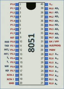
  • 8051 microcontroller PIN Diagram
  • 8051 microcontroller Architecture
  • Memory of 8051
  • Interrupts of 8051
  • Features of a microcontroller
  • Microprocessor vs Microcontroller
  • Applications

What is a Microcontroller?

“A microcontroller is a small computer that consists of processor, internal RAM, ROM or flash, timers, interrupt handler, serial interface, ports & other application-specific devices.”

  • A microcontroller is employed if the memory prerequisite for computations is small and the programs and ports are used for the control and communication purpose.
  • For example i.e., 8051, PIC and ARM are the standard Microcontrollers.
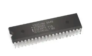
8051
8051 Microcontroller
Image Credit : Konstantin Lanzet (with permission), KL Intel P8051CC BY-SA 3.0

Main Features of 8051 Microcontroller :

  • 8-bit ALU and Accumulator, 8 bit registers, 8 bit data bus and 2×16 bit address bus/program counter/data pointer and related 8/11/16 bit operations.
  • Fast interrupt with operational register.
  • Power saving mode.

Addressing Mode of 8051 Microcontroller:

“An addressing mode denotes by what method addressing a particular memory location.”

There are five important addressing modes in 8051 microcontroller, they are:

1 1

Each of these addressing modes provide important flexibility.

Immediate Addressing

Immediate addressing is like the data to be stored in memory instantly as per the opcode . The instruction itself commands which value might be kept in memories specifically.

E.g., the instruction as follows:

MOV A, #20H

Here memonics utilizes immediate addressing for the reason that the accumulator is going to be filled with the value which mentioned.

In direct addressing,  the value to be loaded is time dependent, this adressing certainly not flexible.

Indirect Addressing

Indirect addressing is a really good comparatively that in most instances contributes an exceptional degree of flexibility. This is by only means to get the additional 128 bytes of internal RAM located in an 8051.  Example is like

MOV A, @R0

This instruction bases the 8051 Microcontroller to have another look at the value of the R0 register. The 8051 will then load the accumulator with the info of internal RAM that’s located at the address indicated by R0 register.

By way of instance, let us say R0 retains the value 50H and address 50H retains the value 66H. When the above-mentioned instruction is implemented the 8051 will assess the value of R0. Since R0 retains 50H, the 8051 will find the value of this internal RAM address 50H and keep it in the accumulator. Indirect addressing consistently identifies internal RAM; it refers to a SFR

External Direct

External memory is get into by means of a set of instructions uses ‘external direct’ addressing. There are two such types of commands that could be used for external direct addressing operations, those are

MOVX A, @DPTR

MOVX @DPTR, A

Here, the two controls use DPTR. In these commands, DPTR should first be loaded using the location of external memory which is to be read or write. After DPTR retains the proper external memory card, the initial command will transfer the contents of the external memory address to the accumulator. The next command is going to do the contrary; it permits to write the accumulator’s value to the external memory address which is already pointed by DPTR.

External Indirect

External memory may be acquired using a indirect addressing that is known as external indirect addressing. This kind of addressing is generally utilized in relatively minor tasks which have a rather modest number of external RAM. Such example is

MOVX @R0, A

The value of R0  has to be read and the value of the accumulator is from external RAM location. Considering that the value of R0 could simply be 00 through FFh, and is limited to 256 bytes. Employing external indirect addressing; nonetheless, it’s normally simpler to use external direct mode if the task has more than 256 bytes.

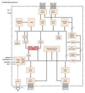
Architecture of 8051 Microcontroller:

  • 8051 is equipped with an 8-bit CPU with a Boolean processor.
  • 5 interrupts.  2 Externals, 2 priority levels.
  • This has two sixteen bit timer/counters.
  • One programmable full-duplex serial port.
  • Total 32 I/O lines.
  • Equipped with the 4 KB of on-chip ROM ; EPROM  is also available in some models.
  • 128 bytes of on-chip RAM, just enough for many single chip.
8051 Architecture
Architecture of 8051 Microcontroller
Image Credit : AppaloosaIntel 8051 archCC BY-SA 3.0

PIN Diagram of 8051 Microcontroller:

8051 Microcontroller
PIN Diagram of 8051 Microcontroller:

8051 Microcontroller PIN Configuration:

PIN 1 to 8

These pins generaly utilized as I/P or O/P according to the user requirements.

PIN 9:

This is utilized as  Resetting purpose; Generally HL signal pin  halts the MCU and clear all the registers. When this pin is back to LO, new program will start.

PIN 10 – 17:

These are utilized as with the port 1, each of these pins could be employed as universal i/p or o/p.

Pin 10:

RXD- Ac as a serial I/P for the asynchronous trasfer otherwise clock output for synchronous mode of operation.

Pin 11:

TXD- Act as a serial O/P for  the asynchronous transfer otherwise clock output for synchronous mode of operation.

Pin 12:

INT0- This is for input interrupt 0

Pin 13:

INT1- This is for input interrupt 1

Pin 14:

T0- This is employed for clock input of the timer 0

Pin 15:

T1- This is dedicated for clock input of the timer 1

Pin 16:

WR- This is for write operation controlling from external RAM memory device.

Pin 17:

RD- This pin is dedicated for read operation to external RAM memory

PIN 18-19:

X2 and X1- These are for input and output  operation of the internal oscillator

PIN 20:

GND- Ground ; This is for grounding the chip.

PIN 21-28:

Port 2- provisional external memory is not present, Port 2 will work as an universal I/O operation.

PIN 29:

PSEN: MCU triggers after reading each byte from the program memory. When an external memory is employed for program storage purpose, then PSEN will be associated with the control operation.

PIN 30:

ALE: This will have important function before external memory reading, MCU will send the lower byte of the address registers to the Port-P0 and triggers the output ALE.

PIN 31:

EA: The LOW signal refer to the Port- P2 and P3 for transporting addresses irrespective of the memory status.

PIN 32-39: 

Port 0: analogous to port 2, pins of port 0 could be utilized as universal I/O. The P0 performs as address O/P if ALE pin is at high state.

PIN 40:

VCC:This is for  +5V  dc power supply.

Interrupts of 8051 microcontroller:

Five interrupts are provided in 8051. Three sets automatically by internal operations and other two is  triggered by external signal linked to pins INT0 and INT1.

Automatic interrupts are:

  1. Timer Flag 0
  2. Timer Flag 1
  3. Serial Port Interrupt (R1 or T1)

Interrupt Name                                          Interrupt Address

Timer Flag o                                                   0 0 0 B

Timer Flag 1                                                   0 0 1 B

INT0                                                                0 0 0 3

INT1                                                               0 0 1 3

Serial Input                                                     R1/ T1                             

Applications of Microcontroller:

  • Microcontroller is employed in Mobile phones, camera circuitry.
  • Microcontrollers are used extensively in Automobile Industry
  • Computer Systems like traffic signal controlling.
  • Different control operation such as heater, greezer,  liftcontrol, Micro-oven etc.

Comparison of Microprocessor vs. Microcontroller:

     MICROPROCESSOR    MICROCONTROLLER
CPUIt has 1 Central Processing Unit It has a Central Processing Unit, Memory, Input-output pins.
USEMicroprocessor is used in personal computers.Microcontroller has applications in embedded system.
INTERFACEMicroprocessor interface is complicated.Simpler Interface
COSTThey are expensiveThey are inexpensive
REGISTERIt has less numbers of registers, operations are mostly memory based.Greater number of registers making it easy for operations.

For more Electronics Articles and question answers related to electronics click here

8279, 8259, PIC 8255 PPI, and 8085 Microprocessors: A Comprehensive Guide

8279 8259 pic 8255 ppi 8085 microprocessors

The 8279, 8259, and 8255 are programmable peripheral devices that play a crucial role in 8085-based microprocessor systems. These devices provide essential functionalities such as data transfer, interrupt management, and keyboard/display interfacing, making them indispensable components in the design and implementation of embedded systems.

8255 Programmable Peripheral Interface (PPI)

The 8255 Programmable Peripheral Interface (PPI) is a versatile, general-purpose programmable device used for data transfer between the processor and I/O devices. It features three programmable I/O ports, designated as PA, PB, and PC, each with a resolution of 8 bits. The 8255 PPI can be programmed to operate in different modes, allowing for flexible and customizable data transfer operations.

Key Features of the 8255 PPI

  1. Programmable I/O Ports: The 8255 PPI has three 8-bit I/O ports (PA, PB, and PC) that can be individually programmed to operate in different modes, such as input, output, or bidirectional.
  2. Flexible Programming Modes: The 8255 PPI can be programmed to operate in one of three modes: Mode 0 (basic input/output), Mode 1 (strobed input/output), and Mode 2 (bidirectional bus).
  3. Interrupt Capability: The 8255 PPI can generate interrupt requests to the processor, allowing for efficient data transfer and synchronization with external devices.
  4. Control Register: The 8255 PPI has a control register that allows for the configuration and control of the I/O ports, including the selection of operating modes and interrupt settings.
  5. Power Consumption: The 8255 PPI has a low power consumption, making it suitable for use in battery-powered or energy-efficient systems.

Programming the 8255 PPI

To program the 8255 PPI, the following steps are typically followed:

  1. Initialize the Control Word: The control word is written to the control register to configure the operating mode, port directions, and interrupt settings.
  2. Set Port Directions: The I/O ports (PA, PB, and PC) are configured as either input or output, depending on the application requirements.
  3. Perform Data Transfer: Data is transferred between the processor and the I/O devices using the configured I/O ports.
  4. Handle Interrupts (if enabled): If the 8255 PPI is configured to generate interrupt requests, the interrupt service routine (ISR) is executed to handle the data transfer or other events.

The 8255 PPI is widely used in 8085-based systems for a variety of applications, such as interfacing with keyboards, displays, sensors, and other peripheral devices.

8259 Programmable Interrupt Controller (PIC)

8279 8259 pic 8255 ppi 8085 microprocessors

The 8259 Programmable Interrupt Controller (PIC) is a crucial component in 8085-based systems, responsible for managing and prioritizing interrupt requests from various peripheral devices. It provides a flexible and efficient way to handle interrupts, allowing the processor to focus on its primary tasks without being overwhelmed by constant interrupt handling.

Key Features of the 8259 PIC

  1. Interrupt Request Lines: The 8259 PIC has 8 interrupt request (IRQ) lines, each of which can be connected to a different peripheral device.
  2. Programmable Interrupt Priorities: The 8259 PIC allows for the programming of interrupt priorities, ensuring that critical interrupts are handled first.
  3. Interrupt Masking: The 8259 PIC provides the ability to mask or disable specific interrupt request lines, allowing the processor to focus on the most important tasks.
  4. Interrupt Vectoring: The 8259 PIC generates an interrupt vector, which is used by the processor to jump to the appropriate interrupt service routine (ISR).
  5. Cascading Capability: Multiple 8259 PICs can be cascaded to support a larger number of interrupt request lines, enabling more complex interrupt management in larger systems.
  6. Programmable Operating Modes: The 8259 PIC can be programmed to operate in different modes, such as the 8086 mode, 8080/8085 mode, and special fully nested mode, depending on the system requirements.

Programming the 8259 PIC

To program the 8259 PIC, the following steps are typically followed:

  1. Initialize the Interrupt Controller: The 8259 PIC is initialized by writing the Initialization Command Word (ICW1) to the control register.
  2. Set Interrupt Priorities: The Interrupt Mask Register (IMR) is programmed to set the priorities of the interrupt request lines.
  3. Enable Interrupts: The 8259 PIC is enabled to start accepting and processing interrupt requests.
  4. Handle Interrupt Requests: When an interrupt request is received, the 8259 PIC generates an interrupt vector, which the processor uses to jump to the appropriate interrupt service routine (ISR).
  5. Manage Interrupt Masking: The Interrupt Mask Register (IMR) can be used to mask or unmask specific interrupt request lines as needed.

The 8259 PIC is essential in 8085-based systems, as it allows for efficient and prioritized handling of interrupt requests from various peripheral devices, ensuring that the processor can respond to critical events in a timely manner.

8279 Programmable Keyboard/Display Interface

The 8279 Programmable Keyboard/Display Interface is a specialized device designed to simplify the interfacing of keyboards and displays with 8085-based microprocessor systems. It provides a standardized and programmable way to handle keyboard input and display output, reducing the complexity of the overall system design.

Key Features of the 8279 Programmable Keyboard/Display Interface

  1. Keyboard Interfacing: The 8279 can interface with a variety of keyboard types, including matrix-encoded keyboards, scanned keyboards, and encoded keyboards.
  2. Display Interfacing: The 8279 can interface with various display types, including 7-segment displays, hexadecimal displays, and alphanumeric displays.
  3. Programmable Operating Modes: The 8279 can be programmed to operate in different modes, such as keyboard mode, display mode, and sensor mode, depending on the application requirements.
  4. Interrupt Generation: The 8279 can generate interrupt requests to the processor, allowing for efficient handling of keyboard input and display updates.
  5. Programmable Scan Rates: The 8279 allows for the programming of keyboard and display scan rates, enabling the system to adapt to different input and output devices.
  6. FIFO Buffers: The 8279 includes First-In-First-Out (FIFO) buffers for both keyboard input and display output, allowing for efficient data handling and reducing the burden on the processor.

Programming the 8279 Programmable Keyboard/Display Interface

To program the 8279 Programmable Keyboard/Display Interface, the following steps are typically followed:

  1. Initialize the 8279: The 8279 is initialized by writing the appropriate command words to the control register, configuring the operating mode, scan rates, and other parameters.
  2. Set up Keyboard Interfacing: The keyboard interface is configured by programming the 8279 to handle the specific keyboard type and encoding scheme.
  3. Set up Display Interfacing: The display interface is configured by programming the 8279 to handle the specific display type and output format.
  4. Handle Keyboard Input: When a key is pressed on the keyboard, the 8279 generates an interrupt request, and the processor reads the key data from the FIFO buffer.
  5. Handle Display Output: The processor writes data to the 8279’s display FIFO buffer, and the 8279 updates the connected display accordingly.

The 8279 Programmable Keyboard/Display Interface simplifies the integration of keyboards and displays in 8085-based systems, allowing for efficient and flexible input/output handling.

8085 Microprocessor

The 8085 microprocessor is an 8-bit microprocessor designed and manufactured by Intel. It is a widely used and well-established processor in the field of embedded systems and industrial applications.

Key Features of the 8085 Microprocessor

  1. 8-bit Data Bus: The 8085 microprocessor has an 8-bit data bus, allowing it to transfer 8 bits of data at a time.
  2. 16-bit Address Bus: The 8085 microprocessor has a 16-bit address bus, which allows it to address up to 64KB of memory.
  3. Instruction Set: The 8085 microprocessor has a comprehensive instruction set, including arithmetic, logical, data transfer, and control instructions.
  4. Interrupt Handling: The 8085 microprocessor supports various interrupt sources, including external interrupts, software interrupts, and hardware interrupts.
  5. Clock Speed: The 8085 microprocessor typically operates at clock speeds ranging from 3 MHz to 6 MHz, depending on the specific implementation.
  6. Power Consumption: The 8085 microprocessor has a relatively low power consumption, making it suitable for use in battery-powered or energy-efficient systems.
  7. Peripheral Interfacing: The 8085 microprocessor can interface with a variety of peripheral devices, such as the 8255 PPI, 8259 PIC, and 8279 Programmable Keyboard/Display Interface, through its I/O ports and control signals.

Programming the 8085 Microprocessor

Programming the 8085 microprocessor typically involves the following steps:

  1. Instruction Set: Familiarize yourself with the 8085 instruction set, which includes arithmetic, logical, data transfer, and control instructions.
  2. Assembly Language: Write programs in 8085 assembly language, which provides a low-level, human-readable representation of the machine code.
  3. Assembler: Use an assembler tool to translate the assembly language program into machine-readable object code that can be executed by the 8085 microprocessor.
  4. Memory and I/O Interfacing: Understand how to interface the 8085 microprocessor with memory and I/O devices, such as the 8255 PPI, 8259 PIC, and 8279 Programmable Keyboard/Display Interface.
  5. Interrupt Handling: Implement interrupt handling routines to respond to external events and manage the flow of execution in the 8085-based system.
  6. Debugging: Use debugging tools, such as emulators and simulators, to test and debug your 8085 programs, ensuring their correct operation.

The 8085 microprocessor is a versatile and widely used processor in the field of embedded systems and industrial applications, and its integration with the 8255 PPI, 8259 PIC, and 8279 Programmable Keyboard/Display Interface provides a powerful and flexible platform for a wide range of applications.

Conclusion

The 8279, 8259, and 8255 programmable peripheral devices, along with the 8085 microprocessor, form a comprehensive and powerful ecosystem for the design and implementation of 8085-based embedded systems. By understanding the key features and programming techniques of these components, electronics students and engineers can develop robust and efficient solutions for a wide range of applications, from industrial automation to consumer electronics.

References

  1. Programmable Peripheral Devices
  2. Microprocessor Unit – Memory Interfacing & IO Interfacing
  3. Programmable Peripheral Interface (8255)
  4. 8259 PIC Help
  5. 8259 PIC Microprocessor

Microprocessor 8085:Registers & Important Addressing Modes

8085 Chip 300x108 1

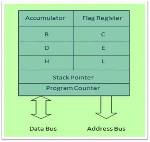
Define Registers of Microprocessor 8085:

A register is a temporary  or short term storage space built into a CPU.”

More or less of the registers are applied internally but they cannot be accessed outside the processor.

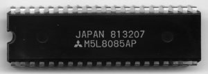
8085 Chip
Microprocessor 8085, Image Crdit – Myself User:ZyMOSIc-photo-Mitsubishi–M5L8085AP–(8085-CPU)CC BY-SA 4.0

What are the Types of the Register in Microprocessor 8085?

  • Accumulator (8 bit)
  • GPR (8 bit)
  • SP (16 bit)
  • PC (16 bit)
  • IR (8 bit)
  • TR (8 bit)
Http scanftree.com microprocessor Architechture Of 8085
Microprocessor 8085 Architecture , Image Credit – Vinay357Http—scanftree.com-microprocessor-Architechture-Of-8085CC BY-SA 4.0

Define Accumulator:

In the microprocessor 8085, accumulator specified as an 8 bit register connected with an ALU. This is utilized to hold one of the operand for arithmetical and logic-operation; it works as input to the ALU. The other operand for arithmetic and logical operation possibly stored either in memory or in GPR. But the final product will be stored in the accumulator only.

Register 8085
Register in Microprocessor 8085

Define General Purpose Register (GPR):

8085 microprocessor has 8 bit GPR; it works like a pair – B-C, D-E, H-L

The H-L register pair is used as a memory pointer & it holds 16 bit address of a memory location.

Define Stack Pointer (SP):

Stack pointer is a 16 bit especial purpose register. Stack is a order of memory location set by a programmer. The stack also perform as LIFO (Last in First Out). Here two operations are used; PUSH & POP.

Program Counter Definition:

A 16 bit register for specified operations ; comprises registers to load memory address from wherever the subsequent instruction is to be fetched.

Assume the program counter contains a memory location 7100H, this imply that microprocessor 8085 intended to fetch the instruction at the location 7100H.

Subsequently fetching the 7100H, the program counter is inevitably increses one count. This has the track of memory address of the instruction.

EXAMPLE: JMP, CALL, RETURN, RESTART etc.

Define Instruction Register:

This is an 8 bit register to hold the OPCODE of the instructions that has to be decode and execute. This is not accessible to the program writer.

Define Temporary Register:

This is a 8 bit non-programmable register utilized to keep data through an arithmetic and logical instruction implementation. TR is keeping intermediate results only and ultimate finalized end result is saved in the accumulator. This  is microprocessor dependendent, not  controlled by developer code.

Addressing Modes of Microprocessor 8085:

What is Addressing Mode?

“Addressing mode is the best way to define a certain data to be controlled by means of an instruction.”

Microprocessor has various kinds of addressing mode as it gives flexibility to the developer to get info and acessing data.

What are the types of Addressing Mode?

There are total five category as follows:

  • The Direct Mode
  • The Register Mode
  • The Immediate Mode
  • The Register Indirect Mode
  • The Implicit Indirect Mode

Direct Addressing Mode (DAM):

In this mode the address of the operand is identified the instruction the aforementioned. Instruction that includes direct address require 3-bytes of storage space of Microprocessor 8085.

  1. Instruction Code
  2. 16 Bit Address

Sample  instruction like STA 2500H stores the content of the accumulator in the memory location noted 2500H. Here 2500H is the address located in memory space where data is has be kept in.

Register Addressing Mode:

Here the operands are GPR. The opcode identifies the address of the register in addition to the operation to be executed.

For example  the instruction MOV A, B will move the data of register B to register A. In other instruction like ADD B, A; will first doaddition operation with the data of register B to register A and the end result is to be stored in register A.

Immediate Addressing Mode:

Here the operands are specified within the instruction itself, that means when any data has to be performed then immediately the operation is executed.

Example – MVI 05

                  ADI 05

Register indirect Addressing Mode:

In this case the operand will be identified by the register-pairs. Here accumulation is not linked directly.

Example are H-L, B-C, D-E etc.

Implicit Addressing Mode:

There are certain instructions which operates on the content of operator. These instructions will not call for address of operand.

Example – JMP, CALL, RAR

Timing Effects of Addressing Modes:

Addressing modes influence both the quantity of time necessary for executing an instruction and the total amount of memory necessary for storing. By way of instance, instructions which use suggested or register fixing, execute quickly because they deal directly with the chip hardware or with information present in hardware registers.

Most significant, however instruction can be fetched using one memory access. The Amount of memory accesses necessary is the factor in determining performance time, more memory accesses thus require more implementation time.

For example, to executing a CALL instruction requires 5 memory entrees;  out of these 3 will be for the access the entire instruction and the 2 will be for PUSHing the contents of the program counter onto the stack location.

The processor can access memory during every processing cycle. Each cycle includes a varying number of states. This is dependent upon the clk freq, and  which might vary from 480 nSec to 2µsec. The 8085 have clk freq around 5 MHz and so a minimal state may be of 200 nanosec.

What is Subroutine?

register

Creating a program of specific operation may happen several occasions and they’re not accessible as individual directions along with the application for such operation replicated over and over. However, the program ought to be written. The idea of subroutine is used to prevent the repetition of this smaller coding. The little program for specified for small job is called subroutine.

Subroutines are composed individually then saved to the primary memory by utilizing RET. CALL  instruction is generally utilized from the primary memory to subroutine.

Instruction Cycle of Microprocessor 8085:

This is the time taken by the microprocessor to finish the execution of the instruction. An instruction cycle usually consists of 1 to 6 machine cycles.

Machine Cycle

It is the time prerequisite to finish an operation through access one or the other the memory or I/O devices. It consists 3-6 T states. Here, opcode fetch, memory read, memory write, I/O read-write, operation executed. In the other word the operation of retrieving either memory devices or I/O devices is termed machine cycle.

T State:

This is the time equivalent to the one clock period in the basic unit used to calculate the time taken for the execution of the instruction and program in the microprocessor.

Fetch Operation:

The very initial byte of an instructionset is the OPCODE. An instruction usually more than 1 byte length. Another byte is for information data or  for the operand address. At the start of the cycle that the info of program counter where opcode can be obtained is forwarded to  the memory. This required  3 clock cycle another one is undefined.

What is the difference between CALL & JMP instructions of of Microprocessor 8085?

After a jump instruction is performed, the address given in JMP instruction is moved to PC. Thus application control is automatically progressed to this place location and carrying out as continued execution.

When CALL instruction is completed, microprocessor first keep PC info in the stack. Subsequently PC is occupied with the address set in the CALL instruction.Hence program control will transfer there.

What is Conditional & unconditional JUMP?

The JUMP commands are two kinds, specifically ‘unconditional jump’ and ‘conditional jump’.  If the microprocessor is indeed initiated to load a new address in the PC and commence instructions in that, it’s termed as an unconditional jump. In the instance of a conditional jump, the PC is loaded with a new address only when certain conditions are created from the microprocessor after reading the correct status of register bits.

For more Electronics related article click here

8085 Microprocessor: Interrupts,Functions & 7 Facts

2

Definition of Interrupt:

“Interrupt is the process of generating a momentary halt during program execution and permits peripheral devices to access the microprocessor”

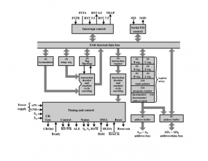
8085 Architecture

Types of Interrupts:

Types of Interrupts according to delay:

  • Maskable
  • Non-maskable

Types of Interrupts according to grouping:

  • Vector
  • Non-vector

Types of Interrupts according to priority:

  • TRAP
  • RST 7.5
  • RST 6.5
  • RST 5.5

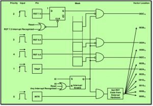
Block Diagram of 8085 Interrupts:

8085 Interrupt
8085 Interrupts

What is masking?

Masking can be implemented for the 4 hardware interrupts- RST 7.5, RST 6.5, RST 5.5 & INTR. In this figure, TRAP is NMI (Non Maskable Interrupt).

RST 7.5 alone has a F/F to recognise its edge transmission. The masking of interrupt can be done using SIM instruction. In additional a separate interrupt enables F/F is available to mask or allow the interrupts.

  • The maskable interrupts are masked by default by means of the reset signal.
  • The interrupt can be enabled by execution of EI instruction. So, to enable interrupts, after resulting the microprocessor the EI instruction must be used in 8085 microprocessor.
  • The 3 RST interrupts could be masked by load up the suitable word variety in the accumulation and implementing SIM instruction. This is known as software-masking.
  • All the maskable interrupts are disabled whenever an interrupt is recognized. So, it is essential to perform EI instruction every single time.
  • Altogether, the maskable interrupts may be disabled by performing DI instructions. The instruction resets an interrupt enable F/F in the microprocessor. For the enabling purpose, instruction EI is utilized.

TRAP:

  • It is non-maskable interrupt such that it need not to be enabled and cannot be enabled or disabled.
  • It is accessible to user
  • It is used for emergency situation such as power failure or energy shut off etc.
  • It is edged as well as level triggered that is the i/p should goes high and stay in this condition to acknowledgement.
  • TRAP has highest priority amongst all.

RST 7.5:

  • Its priority is just after the TRAP.
  • It is maskable such that both EI and DI operation can be possible.
  • It is sued for the situation whose priority is just after emergency situation.
  • It is positive edge triggered interrupt.
  • It can be triggered with a very short duration pulse.

RST 6.5:

  • Its priority is just after RST 7.5.
  • Other specifications are as same as RST 7.5.

RST 5.5:

  • Its priority is just after RST 6.5.
  • Other specifications are as same as RST 7.5.

INTR:

  • INTR is the lowest priority interrupt.
  • This is edge as well as level triggered.
  • Maskable and non-vectored type.
  • Both EI and DI can be possible in this situation.

Operation of INTR:

The signal flow sequence is as follows to INTR goes high.

  1. 8085 authorizations the status of the INTR, for carrying out an instruction.
  2. If INTR signal is 1, then 8085 will complete its present instruction and an active-low interrupt will be acknowledged by an interrupt ACK.
  3. Then the address of next instruction will be loaded in stack and will perform received instruction.

INTA:

  • It is not the interrupt just used by the microprocessor sent the acknowledgement. The process should be enabled by instruction.
  • During T3 condition of the opcode fetch, 8085 checks repeatedly of every instruction. If interrupt finds the microprocessor will complete execution instruction and ready for the restart sequence.
  • The restart sequence resets the interrupt F/F and active INTA upon receiving the signal.
Interrupt Call Locations:

The call locations for 8085 are

TRAP- 0024

RST 7.5- 003C

RST 6.5- 0034

RST 5.5- 002C

SIM Operation (Set Interrupt Mask):

2

SIM (Set Interrupt Mask) for 8085 is explained as follows

M 5.5 – it is basically set to 1 to reset 5.5 mask

M 6.5 – it is also set to 1 to reset 6.5 mask

M 7.5 – it is also set to 1 to reset 7.5 mask

MSE – to mask interrupt

R 7.5 – it is reset RST 7.5 F/F

SDE – serial data enable set to 1 for sending

SOD – serial output data to be sent

EXPLANATION:

  • RST 7.5, 6.5 & 5.5 are maskable interrupts. The instruction EI and SIM utilized for enabling these.
  • BIT 0 to 2 is either set or reset the mask for RST 6.5, 7.5 & 5.5.
  • If a bit is set to 1, then the interrupt is masked off i.e., disable. If set as 0, the respective interrupt is enabled.
  • If bit 3 is set to 1 to mask on bit 0 to 2.
  • BIT 4 is additional control for RST 7.5. If it is set to 1 the RST 7.5 is reset.
  • Bit 6 and 7 are serial output data where bit 6 is to enable SOD and bit 7 may be either high or low. The instruction DI disable all the interrupts.

PENDING REQUEST:

When 1 interrupt request is being served, other interrupts may occur resulting in pending request. When more than 1 interrupt occur simultaneously then interrupt having higher priority has served and interrupt having lower priority remain in the pending condition.

8085 microprocessor has an additional instruction called RIM (Read Interrupt Mask) to sense the pending interrupt.

RIM Operation (Reset Interrupt Mask):

3

RIM (Read Interrupt Mask) for 8085 is explained as follows

M 5.5:  This bit is set to 1 if RST 5.5 is masked. The bit 0 to 2 could be used for interrupt mask utilizing RIM instruction

M 6.5: This bit is set to 1 if RST 6.5 is masked.

M 7.5: This bit is set to 1 if RST 7.5 is masked.

IE:  It is set to 1 if all interrupts are enabled.

I 5.5: It is set to 1 when RST 5.5 is in pending condition.

I 6.5: It is set to 1 when RST 6.5 is in pending condition.

I 7.5:  It is set to 1 when RST 7.5 is in pending condition.

SID:  Serial Input Data; it will be either 1 or 0 for input purpose.

Vectored Interrupts:

TRAP, RST 7.5, RST 6.5, RST 5.5 (call location).

4
5
6

SOFTWARE INTERRUPTS VS HARDWARE INTERRUPT:

         Software Interrupts    

This are the software instructions when they are executed, CPU branches to ISR.

These are slower than the hardware interrupts.

 
Examples – RST 0, RST 1, RST 2 etc.
        Hardware Interrupts    

These are physical input from external devices which causes CPU to branch to ISR.

  These are faster than software interrupts.  


Examples – TRAP, RST 7.5 etc.

What is Stack?

Stack

A stack in 8085 microprocessor is a set of memory location in read-write memory specified by a programmer in a main program. These memory locations are utilized to store binary data momentarily during coding.

The initiation of the stack is defined in the program by executing the basic load instruction such as LXI SP. This generally load a sixteen bit memory address in the SP register.

Types of Stack:

  1. PUSH
  2. POP

PUSH – In the course of execution, PUSH is required to resolve the problem of certain register since the registers are prerequisite for some additional execution in consequent state. These contents move to certain memory location by a special function register is called PUSH.

Example-

                LXI SP, 2099 H

               LXI H, 42F2 H      

               PUSH H

  1. Loads the contents of 2099H with SP register that is reserved in read-write memory as a state and the location begins from 2098H in moving upward for temporary storage.
  2. LXI H, 42F2H describes the loading of H-L pair i.e., (42) is loaded in H and F2 is loaded in L.
  3. PUSH H indicates that the content of H i.e., 42 stored in 2098H and the content of L i.e., F2 is stored in 2097 H.

POP – After completion of this operation this content which are saved in the temporary register are transferred back to the main memory by the operation of POP.

 Example –

                          LXI SP, 2099 H

                          LXI H, 42F2 H

                          PUSH H

                          DELAY COUNTER

                          POP H

The contents of register H-L pair are not destroyed. It is available of the delay counter in the content of the program counter. The content of the top stack location shown by SP appear into the register L and SP will increase 1.

The content of top of stack i.e., 2097 is shifted to 2098 and 2099 by 1 incarnated and from the temporary register the contents move to the main register.

For more about 8085 microprocessor click here

8085 Microprocessor | It’s important pins and their functions

1 2 1


CONTENTS

  • Introduction to 8085 microprocessor
  • The main features of 8085 microprocessor
  • BUS architecture of 8085 microprocessor
  • What is OPCODE & OPERAND?
  • Different Sections of 8085 microprocessor
  • 8085 Pin Diagram
  • Working of different pins

Introduction to 8085 Microprocessor:

8085 Microprocessor

The 8085 is an 8-bit programmable microprocessor chip which was first designed by INTEL in the year 1977 utilizing NMOS transistors.

The main features of 8085 microprocessor are:

  • This has total 40 pin.
  • Clock (CLK) speed frequency 3-5 MHz
  • The 8085 microprocessor is equipped with sixteen address lines, and eight data lines. So, 8085 is termed an 8 bit microprocessor depending upon its database.
  • Requires +5V supply to operate.

BUS Architecture of 8085 Microprocessor:

Various I/O devices & memory device are connected to a CPU by group of lines or wires, these are called BUS.

There are three categories of BUS:

ADDRESS BUS 

  • When the address is sent by CPU, all devices are connected to CPU through address BUS and receives this address but only the device will respond which also receives chip enable signal from CPU. Address BUS is Unidirectional.

DATA BUS

  •  It carries data values from microprocessor through a memory cell or a peripheral part (memory or I/O write / memory or I/O read). Data BUS is Bidirectional. So, information flows in both way between 8085 microprocessor & memory or I/O device.

CONTROL BUS

  •  It carries control signal in between Central Processing Unit, memories Input / Output devices. It is also Bidirectional.
1 2
2 3

I/O M̅When the signal is high (logic 1) then CPU wants to communicate with I/O device but when signal goes low (logic o) then CPU will communicate with memory.

R̅D̅ – When CPU sends a low R̅D̅ signal the activated device understands that CPU wants to read information from another device or memory.

W̅R̅T̅ – When CPU sends a low W̅R̅T̅ signal the activated device understands that CPU wants to write information to memory or another device.

What is OPCODE & OPERAND?

OPCODE:

An OPCODE is a signal instruction that can be executed through CPU, without help of opcode any instruction cannot be defined individually.

Example – MOV A, B

Here, MOV means Move, so MOV is OPCODE.

OPERAND:

OPERAND describes an operation such that add, sub, mov on which the operations have to be performed.

Example – MOV A, B

Here, the content of REG B moves to the content of REG A.

Read more about Important Peripherals of 8085 Microprocessor

What are the different sections of 8085 Microprocessor?

There are three categorical area in the 8085 microprocessor;

ALU:

  • This section performs the operation of subtraction, addition of logical NOR, compliment, right shifts, left shifts etc.

REGISTER:

  • Registers are used for temporary storage of data insertion; it has following register,
  • 8 BIT accumulator
  • 8 BIT General Purpose Register (B-C, D-E, H-L)
  • One 16 BIT Stack Pointer
  • One 16 BIT Program Counter
  • Instruction Reg, Status Reg, Temporary Reg

TIMING & CONTROL:

  • These is primarily responsible for the time & control signal generation which are utmost essential for completing the instruction operation. It can control the data flow between CPU & peripheral device & it provides the timing signal for the operation of memory & I/O devices.

Examples of instructions:

  • 1 BYTE Instruction – MOV B, C
  • 2 BYTE Instruction – MVI B, 05
  • 3 BYTE Instruction – LHLD 5000H

PIN Diagram of 8085 Microprocessor: 

The below image represents description of PINS of a 8085 microprocessor.

PIN Diagram of 8085 Microprocessor
PIN Descriptions of 8085 Microprocessor
I/O M̅S1S0OPERATION
000Halt
001Memory write
010Memory read
011Fetch
100Halt
101I/O write
110I/O read
111Fetch
4 2

Descriptions of the Pins of 8085 Microprocessor:

A8 – A15:

  • These address buses are used to be most significant bits of the memory address of 8 bit I/O device.

AD0 – AD7:

  • When the address is multiplexed with the data then it is called AD Bus. The lower order or low significant bus as well as the data bus are used for memory address or I/O address.

ALE

  • The ALE pin is activated for the first cycle & enable to lower 8 bit of the address data bus to be latched (logic 0) & when ALE is logic 1 then address bus is activated.
I/O M̅S1S0OPERATION
000Halt
001Memory write
010Memory read
011Fetch
100Halt
101I/O write
110I/O read
111Fetch

I/O M̅:

  • It is a status signal for memory as I/O device. When the signal goes high it operates for all I/O devices. When the signal goes low, it works for memory.

R̅D̅:

  • It is a signal to control read operation; when the signal is low then it reads the data from I/O device or O/P device.

W̅R̅T̅:

  • It is the specified write control signal. This signal specifies the data on the data bus will be written into a designated memory or I/O device.
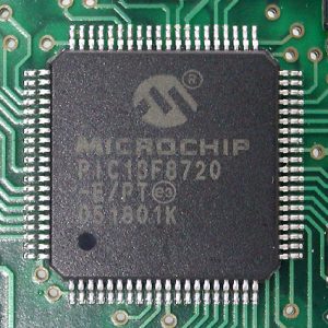
READY:

  • It is active high I/P control signal. It is employed by µP to identify whereas a peripheral has finished the data transfer or not.
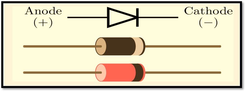
HLDA:

  • This is the hold acknowledgement signal which is used for granting the hold request.

INTERRUPT:

  • TRAP: It has the highest priority over all the interrupts. If any emergency situation comes then it will work.
  • RST 7.5: The next priority after TRAP is RST 7.5
  • RST 6.5: The next priority after RST 7.5 is RST 6.5
  • RST 5.5: The next priority after RST 6.5 is RST 5.5

INTR R:

  • It is an interrupt request used as general purpose interrupt. It has the lowest priority.

I̅N̅T̅A̅:

  • This signal is interrupt acknowledgement; is used to acknowledge all the interrupts.

RESET IN:

  • If the signal on this pin goes LOW, then the device program counter is being set to zero and when it is up it is in reset condition.

RESET OUT:

  • This signal designates the up is being reset and be utilized as to reset a memory device and input output devices.

SID:

  • Serial I/P data is the data line for signal i/p which is loaded into the accumulator’s 7th bit location.

SOD:

  • Serial o/p data is the 7th bit of the accumulator is o/p on the SOD line.

X1 – X2 [clock input]:

  • These are two input perform as a clock input.

CLOCK O/P:

  • The frequency is the same in which process operate.

VCC & GND:

  • VCC is connected to +5V; and GND pin is Grounded.

For more Electronics related article click here

Microcontroller Vs Microprocessor: 7 Facts You Must Know

1 1 300x152 1

C O N T E N T S

  • What is a Microprocessor?
  • Microprocessor Definition
  • What is BIT, BYTE, Nibble and Ward?
  • Hardware of a Microprocessor
  • Block diagram
  • Important features of Microprocessor
  • Characteristics of Microprocessor
  • What is ALU?
  • Differences between ALU and CPU
  • Memory Organization in Microprocessor
  • Types of processors used in a Microprocessor
  • Applications of Microprocessor
  • What is a Microcontroller?
  • Features of Microcontroller
  • Types of Microcontroller
  • Microcontroller vs Microprocessor

What is a Microprocessor?

Microprocessor Definition:

“Microprocessor is a programmable circuit driven register based, multipurpose semiconductor, i.e., manufactured on LSI or VLSI technique. It takes binary instructions from input devices, processes the instruction & outputs the originals and can store the information”.

Microcontroller vs Microprocessor

Hardware of a Microprocessor:

  • It is the interconnection of several peripheral in such a manner, so that it can perform a particular operation.
  • Microprocessor 8085 was found in 1976 & Microprocessor 8086 was found in 1978.

What is BIT?

The possible value of a logical variable which may or not stand for numerical digit of the binary number system is called BITs.

What is BYTE?

In binary number system a group of 8 bit are called BYTE.

                          1 BYTE = 8 BIT

What is Nibble?

A group of 4 BITS are called Nibble.

                          1 Nibble = 4 BIT

What is Ward?

An array of disk which together convey an item of information is called a Ward.

                          1 Ward = 16 BIT

                          1 Long Ward = 32 BIT

                          2 BYTE = 1 Ward

What are the features of Microprocessor 8085?

Characteristics of Microprocessor:

  • It is 40 pin IC.
  • It is NMOS technology, LSI chip.
  • Clock (CLK) speed frequency 3-5 MHz.
  • 8085 has sixteen bit (16) address lines, and eight bit (8) data lines. So, the 8085 is called an 8 bit microprocessor depending upon database.

Microcontroller vs Microprocessor

What are the limitations of microprocessor 8085?

Disadvantages of 8085:

  • Low speed.
  • Low memory capacity.
  • Limited number of GPR (General Purpose Register).
  • Less powerful instruction.

Memory Organization in Microprocessor:

Microcontroller vs Microprocessor: Memory Organisation
Microcontroller vs Microprocessor Image – 1
  • Microprocessor is one of the utmost key component of modern computer. It acts as a brain of computer system. A digital computing is a programmable machine. Its main components are i/p, CPU, memory, o/p device.
  • The CPU executes the instruction. The i/p device is used to fetch programme & data to the computer.
  • The memory is the storage device that stores data programme, results etc.
  • The o/p device display programmes, data or results according to their instructions given to the computer. The CPU built on a single IC which is called the MICROPROCESSOR.
  • A digital device in which microprocessor is in case to operate as a CPU is known as MICROCONTROLLER.

Microcontroller vs Microprocessor

Microprocessor Applications:

Microprocessors are widely used in-

  • Different household devices like thermostats, high end coffee makers, washing machines etc.
  • Microprocessor has various industrial applications like cars, boats, heavy machinery, elevators etc.
  • In cell phones, VCR, televisions microprocessor is used numerously.

Types of Microprocessor:

16 BIT Microprocessors-

  • 8086 (Clk speed 4.7 MHz – 10 MHZ);
  • 8088 (Clk speed more than 5 MHz);
  • 80186,80188 (Clk speed 6 MHz);
  • 80286 (Clk speed 8 MHZ);

32 BIT Microprocessors-

  • INTEL 80386 (clk speed 16 MHZ – 33 MHz);
  • INTEL 80486 (clk speed 16 MHz – 100 MHZ);
  • PENIUM (clk speed 66 MHz);

64 BIT Microprocessor-

  • INTEL CORE-2 (clk speed 1.2 GHz – 3 GHz);
  • INTEL i7 (clk speed 3.3 GHz – 66 GHz);
  • INTEL i5 (clk speed 2.4 GHz – 3.6 GHz);
  • INTEL i3 (2.93 GHz – 3.33 GHz);
Microcontroller vs Microprocessor
Intel C8086 processor , Microcontroller vs Microprocessor, Image – 2
Photo By – Thomas NguyenIntel C8086CC BY-SA 4.0

Types of processors used in a Microprocessor:

Reduced Instruction Set Computer (RISC) –

An advanced processor circuit consists of RISC architecture. RISC provides improved performance. A RISC has a few addressing modes only. It executes most instructions in a single clock style. Instruction executes by a hardwired implementation. Arithmetic & logic instructions access the operands in multiple register sets, windows or files. This greatly reduces dependency on the external memory accesses for the data.

Complex Instruction Set Computer (CISC) –

CISC has the ability to process complex instructions and complexioned data sets with the smaller number registers and simpler hardwired logic, and use of control memory. CISC be responsible for for a large number of address mode.

CISC may have the addressing modes such as indirect, auto index, index relative addressing modes for the data transfer, logic and arithmetic instructions. Some CISC have reliance on the external memory admittances for data in several addressing modes.

What is ALU?

In computing system, the ALU is a digital circuitry which can perform various mathematical operations.


Differences between ALU and CPU:

 Arithmetic Logic Unit (ALU)Central Processing Unit (CPU)
Full FormALU is the Arithmetic Logic Unit.CPU is Central Processing Unit.
UseALU performs all the arithmetic operations specified to the computer.CPU carries different instructions of a computer program to compute different processes i.e., arithmetic, logical, control & input output operations.
DependenceALU depends on the central unit for the for its functionThe control unit does not depend on anything like ALU.
FunctionsALU takes instructions from control unit and gives result accordingly.Control unit provides instruction to the arithmetic unit to perform.
Microcontroller vs Microprocessor, Table -1

What is a Microcontroller?

Definition of Microcontroller:

“A microcontroller is a device which is made up of microprocessor, Random Access Memory, Read Only Memory, timer, input-output pins and several other device.”

Features of Microcontroller:

Different units of Microcontroller (8051):

  • It has a 12 MHz clock, processor instruction cycle time is 1µs.
  • Microcontroller 8051 has 8 bit arithmetic logic unit.
  • Its internal bus width is 8-bit.
  • It has CISC architecture.
  • Microcontroller 8051 also equipped with a stack pointer.
  • The 8051 equipped with two external interrupt pins, INT0 & INT1.
  • Special Function Register is present in the 8051 microcontroller family.

Block Diagram of Microcontroller:

Microcontroller vs Microprocessor
Microcontroller vs Microprocessor, Image – 3

Types of Microcontroller:

  • PIC Microcontroller;
  • ARM Microcontroller;
  • 8051 Microcontroller;
  • AVR Microcontroller;
  • MSP Microcontroller;
Microcontroller vs Microprocessor
A PIC Microcontroller, Microcontroller vs Microprocessor, Image – 4

Applications of Microcontroller:

Microcontrollers are used widely in-

  • Mobile phones
  • Automobile Industry
  • Cameras
  • Computer Systems
  • Micro Oven etc.

Comparative analysis between Microprocessor and Microcontroller:

Microcontroller vs Microprocessor

     MICROPROCESSOR    MICROCONTROLLER
CPUIt consists of only one CPU.  It consists of a CPU along with memory, I/O all integrated into one chip.
USEMicroprocessor is used in personal computers.Microprocessors are typically used in any of the computational devices or remote controlled systems.
INTERFACEMicroprocessor interfaces are complex.Microcontrollers are straight forward with fewer instructions to execute.
COSTThey are expensiveThey are inexpensive
REGISTERIt has fewer number of register and the operation in it is mainly based on the memory.Here Registers are greater in number. That is why it is more convenient to write programs.
Microcontroller vs Microprocessor, Table – 2


For more Electronics related article click here

25 Important MCQ On Diode(Read This First!)

Diode symbol

1.  A Varactor Diode performs as

  1. A variable resistor
  2. A variable capacitor
  3. A switching device
  4. none of these

Answer – (2)

2.  When PN junction diode is forward bias, forward current is dominated by

  1. The diffusion current
  2. The displacement current
  3. The drift current
  4. The drift or diffusion current

Answer – (1)

3.  Storage capacitance in the PN junction is due to

  1. The majority carriers
  2. The minority carriers
  3. The majority and the minority carriers, equally
  4. None of these

Answer – (3)

4. A varicap is worked in

  • The reverse biasing condition
  • The forward biasing condition
  • Without biasing condition
  • None of these

Answer – (1)

5.   Which has -ve resistance region of operation?

  1. The Zener type
  2. The Tunnel type
  3. The photodiode
  4. The LED

Answer – (2)

6.   IMPATT diode is

  1. A negative conductance microwave device
  2. A high frequency rectifying device
  3. A degenerate semiconductor device
  4. A bulk negative differential conductance device

Answer – (1)

7.   Operation of Gunn diode is explained with

  1. The transferred electrons effect
  2. The avalanche transmit time effect
  3. The tunneling effect
  4. The Schottky effect

Answer  – (3)

8.   Tunnel Diode is employed in

  1. The Micro-wave Oscillator design
  2. The RF Oscillator design
  3. An audio oscillator design
  4. A Video amplifier design

Answer – ( 3 )

9.   Reverse saturation current of the PN junction diode is working as

  1. The diffusion current
  2. The drift current
  3. The displacement current
  4. None of these

Answer – (2)

10.    I is PN junction diode forward current. Diffusion capacitance is proportional to

  1. I1/2
  2. I3/2
  3. I
  4. I2

Answer – (1)

11.    Zener effect is operated at

  1. high reverse voltage and for heavily doped junction
  2. low reverse voltage and for heavily doped junction
  3. high reverse voltage and for lightly doped junction
  4. low reverse voltage and for lightly doped junction

Answer – (2)

12.    IMPATT diode works by the mechanism of

  1. electron tunneling
  2. transferred electrons
  3. avalanche multiplication
  4. none of these

Answer  – (1)

13.    The Schottky diode is used in high speed operation because of

  1. small current potential
  2. high speed of electrons
  3. small size
  4. insignificant storage delay

Answer – (2)

14.    Gun diode is utilized in

  1. The microwave oscillator
  2. The RF oscillator
  3. An audio oscillator
  4. An audio amplifier

Answer – (1)

15.    Zener diodes are

  1. specially doped PN junction
  2. normally doped PN junction
  3. lightly doped PN junction
  4. none of these

Answer – (1)

Diode symbol

16.    Diffusion current in a PN junction is influenced by

  1. concentration gradient of carriers
  2. applied voltage
  3. concentration of carriers
  4. none of these

Answer – (1)

17.    If a voltage (+ve.) is connected to an n-type semiconductor through the metal plate, the barrier in between

  1. Will increases
  2. Will decreases
  3. Will remains same
  4. none of these, will happen

Answer – (1)

18. We can connect photodetector diode in

  1. both in forward bias and reverse bias
  2. forward bias
  3. reverse bias
  4. no need to connect any bias

Answer – (3 )

19.    In photodiode, electron- hole pairs are engendered, if

  1. The energy of incident photon (hf) < Eg
  2. The energy of incident photon  (hf)> Eg
  3. The energy of incident photon (hf) = Eg
  4. The energy of incident photon  (hf) >> Eg

Answer – (2)

20. Solar cell works in

  • I-Quadrant
  • IV-Quadrant
  • II-Quadrant
  • III-Quadrant

Answer – (2)

21.    Avalanche breakdown primarily be influenced by the phenomenon of

  1. The impact ionization
  2. The field ionization
  3. The particle collision
  4. The impurity doping

Answer – (1)

22.    The Solar Cell’s V-I plot Quadrant will be at

  1. I
  2. II
  3. III
  4. IV

Answer – (4)

solar cell

23.    Which of the following type does not possess a negative resistance region in its characteristics?

  1. The Tunnel type
  2. The Gun type
  3. The Zener type
  4. The IMPATT type

Answer – (3)

24.    What will be the reading of voltmeter, if it is connected using an unbiased Germanium PN junction diode?

  1. 0 Volt
  2. 0.3 Volt
  3. 0.6 Volt
  4. 1.0 Volt

Answer – (1)

25.    Photodetector is following

  1. triangular device
  2. square law device
  3. linear device
  4. both a & b

Answer – ( 3 )

26.    LED works on the principle of

  1. photoluminescence
  2. electroluminescence
  3. cathodoluminescence
  4. radioluminescence

Answer – (1)

27.    PIN diode has

  1. p and n layers separated by 1 layer
  2. p+ and n+ layers separated by 1 layer
  3. p- and n- layers separated by 1 layer
  4. either b or c

Answer – (2)

28.    A voltage variable capacitance can be realized in

  1. The Avalanche type
  2. The Zener type
  3. The Schottky type
  4. The Varicap or varactor type

Answer – (4)

29.    In a voltage regulator circuit, the maximum value

  1. 2.5 mA load current
  2. 0.9 mA load current
  3. 1.6 mA load current
  4. 3.4 mA load current

Answer – (4)

30.    The Varicap are ordinarily used

  1. As a voltage controlled capacitance circuitry
  2. as a constant current source
  3. as a voltage multiplier circuitry
  4. as a constant voltage source

Answer – (1)

diode

To know more about diodes click here

For more Electronics related article click here