UFT Tutorial:Actions,Function Library,Cracking The Code

Action Parameters UFT Interview Questions and Answers

Testing is now an important phase of the software development life cycle to secure the product’s quality. Also, using of untested product can cause the business loss due to faulty coding.

Here automation is playing an essential role in the testing cycle to reduce the efforts and time. There many tools are available for test automation. But, if we consider the broad application coverage, Unified Functional Testing(UFT) tool is very popular for test automation. 

In this topic, we are going to learn about the UFT Actions, steps to working with actions, UFT function library and library creation steps.

UFT Tutorial – Table of Content

UFT Tutorial #1: UFT Overview

UFT Tutorial #2: UFT Setup – Download, Install, License Configuration and ALM Connection

UFT Tutorial #3: UFT Object Repository

UFT Tutorial #4: UFT Actions & Function Library 

UFT Tutorial #5: UFT Parameterization 

UFT Tutorial #6: VB Scripting in UFT

UFT Tutorial #7: Step by Step Guide to Create Test Case in UFT

UFT Tutorial #8: Exception Handling in UFT

UFT Tutorial #9: Recording in UFT with Checkpoints & Dictionary Object 

UFT Tutorial #10: UFT Interview Questions and Answers 

UFT Actions and UFT Function Library

UFT Actions:

The UFT action component is acted as a container for writing the scripts. The UFT actions allow us to break the entire automated functionalities into small modules. Any automated test cases should have at least one action by default. But, we can use more than one action based on the test design.

Different parts of an Action: 

The overview of different sections which are available in UFT actions are explained below –

Scripting Area – This section contains the actual test scripts.

Local Object Repository – The technical information of test objects are kept here.

Local DataTable – We can store the test data here which will be used in the test script. It’s similar to the excel sheet.

Properties – Through this section, we can pass the test data as input and read the output.

Classification of UFT Actions: 

The UFT actions can be classified into below three types –

Non-Reusable Actions: This types of actions are treated as the private action for the test script. Thus it cannot be referred from the out side.

Reusable Actions:  The reusable actions are treated as a shared action which can be referred from outside. It is used to share the automated common functionalities with the multiple test cases. During the action creation, the reusable checkbox need to be checked to make it as a reusable component. There is two options are available while referring the reusable actions from external places. The options are “Call to an Existing Action” to link the action or “Call to Copy of an Action” to copy the entire action. The primary purpose is to increase the concept script reusability for better maintenance of test cases.

External Actions: When an action has been called from a different action, is called as external action.

Reusable and Non-Reusable UFT ActionsDifferences: 

The scope of non-reusable action is within the same test script, but reusable actions can be accessed from outside test cases.

The non-reusable action is used to create logic of the functional test case, but reusable actions are used to create the reusable components.

Action Parameters: 

The action parameter defines the different input-output data parameters. The input parameters are used to pass the input test data while calling the action and the output parameters are used to return the data from the action to the called actions. We can define the action parameters from the action property section. Two types of action parameters can be defined which are –

Input Parameter – It’s used to pass value to the action as arguments.

Output Parameter – It’s used to return the values from action.

The below example shows the use of input and output parameters of the action –

RunAction “subAction“, oneIteration,inputValue1,inputValue2, outputValue

Here, we are sending the input data through the variables inputValue1 and inputValue2 . From the calling action, the input parameter’s value can be read using Parameter(“inputParam1”) and Parameter(“inputParam2”). Also, the parameter outputParam is used to return the data from action “subAction” through the variable outputValue.

Action Parameters - UFT Interview Questions and Answers
Action Parameters

UFT Actions with Object Repository:

By default, every action contains one local object repository. So the action can use objects from the local repository. Also, we can use any shared object repository to make it more reusable. It is advisable to use a shared object repository for reusable actions. 

Steps to Associate Shared Object Repository: The steps to associate repository are mentioned below – 

Step1# Rightclick on the action icon from the solution explorer section and click on “Associate repository with action” link.
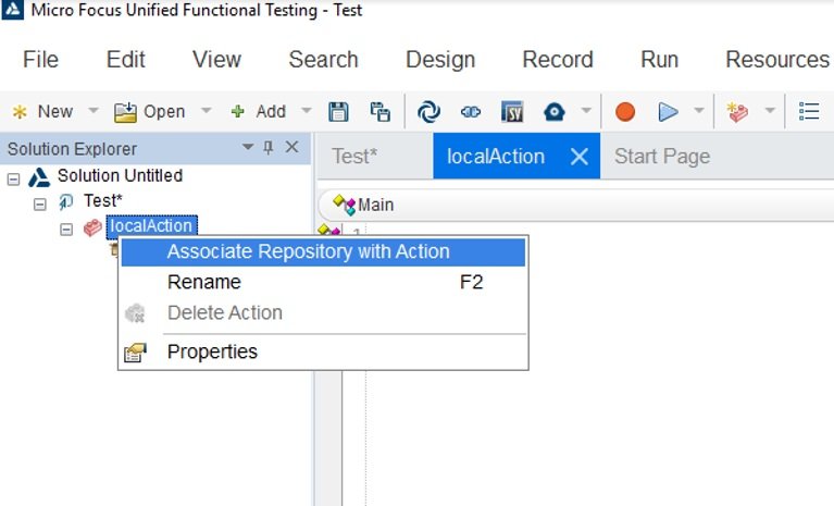
UFT Actions - Associate Repository - Step1
UFT Actions – Associate Repository – Step1

Step2# Local the path for the shared object repository and click on “Open” button.
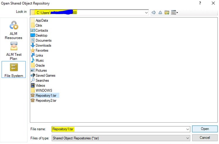
UFT Actions - Associate Repository - Step2
UFT Actions – Associate Repository – Step2

Step3# Confirm the “Automatic Relative Path Conversion” dialogue to complete the process. It’s an optional step.

Step4# The the associated shared repository is visible in Solution explorer section. Also, we can open it as the read-only mode by double-clicking on it.

UFT Actions - Associate Repository - Step3
UFT Actions – Associate Repository – Step3

UFT Actions with DataTable: 

Another important component of a UFT action is datatable, which is similar to Microsoft Excel sheet. Datatables are used to store data which are used in test cases. 

The UFT datatables are classified into two categories. Those are explained below –

  • Local datatable – The every UFT actions are contain one default datatable. This datatable is known as local datatable. The data available in datatable, can be read or update throughout the actions within same test case. The syntax to access the data are,

DataTable.Value(“Param1”,dtLocalSheet) or DataTable.Value(“Param1”,”SheetName”)

Here, dtLocalSheet is only applicable while trying to access the datatable from the container action.

  • Global datatable – Apart from local datatable, every test case contain one default datatable which is known as Global datatable. It can be accessed across all the actions using either of the below syntax –

DataTable.Value(“Param1”,dtGlobalSheet) or DataTable.Value(“Param1”,”Global”)

DataTable - UFT Interview Questions and Answers
DataTable – UFT Actions

As per the dataTable structure which is shown in above diagram, the script to update data in 2nd row of column “Param1” from column “Param2” of “mainAction” dataTable, will be looks like below –

'Copy data from Param1 to Param2 column.
DataTable.GetSheet(“mainAction”).SetRowCount(2)
myVar = DataTable.value(“Param2”,“mainAction”)
DataTable.value(“Param1”,“mainAction”) = myVar

Working with UFT Actions:

Three different operations can be performed with the actions – 

  • Call to New Action – Create a new action.
  • Call to Copy of Action – Create a new action by copying areusable action
  • Call to Existing Action – Calling an existing reusable action as a reference.

Call to New Action:

Step1# Click on navigation “Design-> Call to New Action” to open new action creation window.
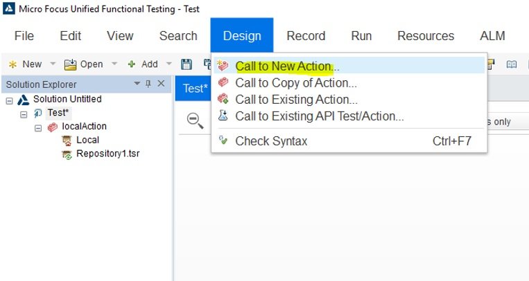
UFT Actions - Call to New Action - Step1
UFT Actions – Call to New Action – Step1

Step2# Enter below details and click on OK to create a new action.

Name – We need to provide the name of the action.

Reusable Action – We need to check it to make the action as reusable.

Description – It’s an optional field to provide a description of the action.

Location – This field defines the position of new action to be placed after creation. 
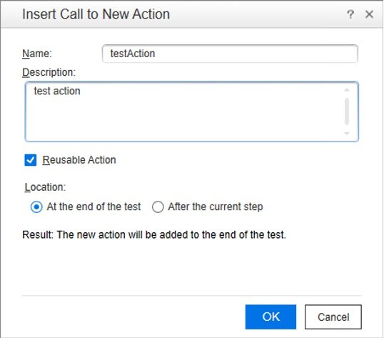
UFT Actions - Call to New Action - Step2
UFT Actions – Call to New Action – Step2

Step3# Action is created and available in the Solution Explorer section. Now click on “Add” button from Properties section(Parameter tab) to create parameters. After providing the name of Input or Output parameters to create it.

UFT Actions - Call to New Action - Step3
UFT Actions – Call to New Action – Step3

Call to Copy of Action:

Step1# Click on navigation “Design-> Call to Copy of Action” to open “Select Action” Dialogue window.

Step2# Enter below details and click on OK to create a new action.

From Test – Need to select the container test case for the source reusable action which will be copied.

Action – We can choose the target action from the list box options.

Action Description – It’s an optional field to provide a description of the action.

Edit new action properties – We need to check it if we want to edit the properties.

Location – This field defines the position of new action to be placed after creation. 
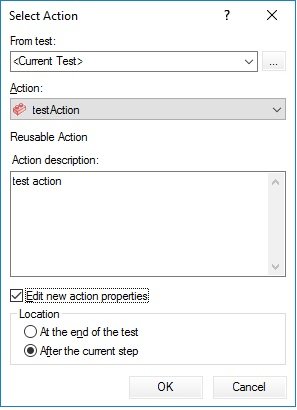
UFT Actions - Call to Copy of Action - Step2
UFT Actions – Call to Copy of Action – Step2

Step3# Edit the properties such as name, parameters, descriptions etc.

UFT Actions - Call to Copy of Action - Step3
UFT Actions – Call to Copy of Action – Step3

Step4# Click OK to create the action.

UFT Actions - Call to Copy of Action - Step4
UFT Actions – Call to Copy of Action – Step4

Call to Existing Action:

Step1# Click on navigation “Design-> Call to Existing Action” to open “Select Action” Dialogue window.

Step2# Enter below details and click on OK to create the reference of reusable action.

From Test – Need to select the container test case for the source reusable action which will be copied.

Action – We can choose the target action from the list box options.

Action Description – It’s an optional field to provide a description of the action.

Location – This field defines the position of new action to be placed after creation. 
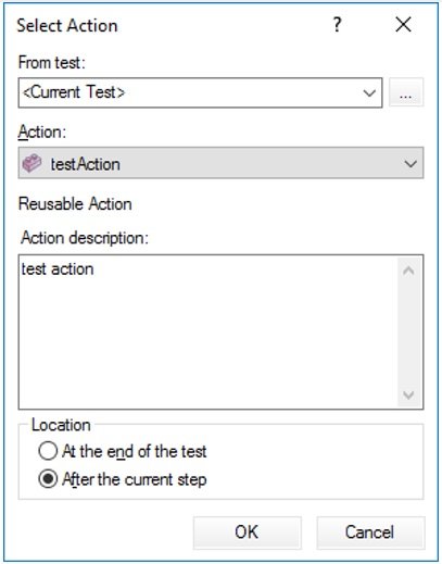
UFT Actions - Call to Exsiting Action
UFT Actions – Call to Exsiting Action

Step3# Reference of existing reusable action will be showing below –

RunAction “testAction”, oneIteration

UFT Function Library: 

Overview of Functions: 

A function is a logical block of instructions. UFT supports the vbscripting. So, we can follow the guidelines to create functions in UFT. Any kind of conditional, logical or looping statements can be developed through the functions in UFT which can be reused from any place. Even, we can automate the functional steps through the functions with the help of shared object repository. It’s always advisable to write the functions in UFT function library which is stored in a external path. By associating the function library, we can access any of the functions from any of the UFT test cases.

As UFT allows to develop the functionality, we can replace any reusable action with the help of functions and shared object repository.

Limitations: 

The limitations are explained below for the function library.

  • By default, the UFT function library has no dataTable or object repository..
  • The UFT functions can not be executed as a standalone. To execute it, it has to be called from any action.
  • The function library is an optional component of UFT.
  • Always, we need the help of shared object repository or descriptive programming approach to automate any application functionalities.

Functions and UFT Actions – differences:

  • The functions are not build with default object repository and dataTable. But the UFT actions have both the default component.
  • The functions can not be executes as an individual component but any action can be executed stand alone.
  • It is easy to maintain the functions with compare to actions.
  • The use of multiple action can increase the weight of the test scripts which impacts the test execution. But, functions are light weighted which helps to improve the performance.
  • Actions are the mandatary component but functions are optional.

Overview of UFT Function Library:

UFT Function Library is the container of the functions. The user functions can be written in the function library using VBScripting coding method. If we want to work with objects, we need to use the shared object repository. 

Steps to create the UFT Function Library:

Step1# Use the menu option “File->New->Function Library” or “Shift+Alt+N” to open the function library cretion dialogue.

Step2# Enter the location and file name to create the function library with qfl extension. 
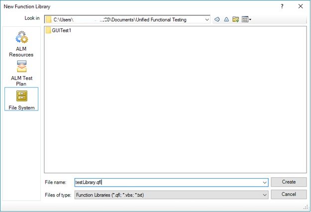
UFT Function Library Creation Step2

Step3# Now, we need to associate the function library in the current test case by clicking on the “Associate Function Library with Test” option.

UFT Function Library Creation Step3

Step4# The function library is now showing under the Solution explorer section. We can write our function using Vbscripting in the library. 
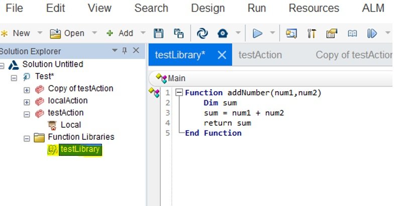
UFT Function Library Creation Step4

Conclusion:

In this article about UFT Actions and function library, we have learned about about uft actions, classifications and step by step guidance to create different types of UFT Actions and UFT Function Library. Click here to understand more from the Microfocus support portal. If you want to get the flavors of frequently asked UFT interview questions, please click here.

Photocell Sensors: A Comprehensive Guide for Science Students

photocell sensors

Photocell sensors, also known as photoresistors, are devices that change their electrical resistance when exposed to light. These sensors are widely used in various applications, such as street lighting, security systems, and light-based control systems. Understanding the technical details and characteristics of photocell sensors is crucial for science students who are interested in exploring the field of optoelectronics and sensor technology.

Understanding Photocell Sensors

Photocell sensors work on the principle of the photoelectric effect, where the resistance of the sensor material decreases when exposed to light. This change in resistance is proportional to the intensity of the incident light, allowing the sensor to detect and measure the amount of light present.

Spectral Sensitivity

One of the key characteristics of photocell sensors is their spectral sensitivity, which refers to their ability to respond to different wavelengths of light. Most photocell sensors consist of discrete red (R), green (G), and blue (B) sensors, each with its own unique sensitivity curve. The spectral distribution of the light source can significantly affect the sensor’s response, as different light sources have varying spectral characteristics.

For example, incandescent lights are a reasonable approximation of a blackbody emitter, with a continuous spectrum. In contrast, LED and fluorescent light sources typically do not have a continuous spectrum, which can impact the sensor’s performance.

To understand the spectral sensitivity of a photocell sensor, we can use the following equation:

R = R0 * (1 + k * Φ)

Where:
– R is the resistance of the photocell sensor
– R0 is the dark resistance of the sensor
– k is the spectral sensitivity coefficient
– Φ is the incident light flux

The spectral sensitivity coefficient, k, is a function of the wavelength of the incident light and the specific characteristics of the sensor material.

Angular Response

Another important factor to consider when using photocell sensors is their angular response, which describes the sensor’s sensitivity to light coming from different angles. The angular response is partly a property of the sensor itself and partly a property of any diffusers or optics in front of the sensors.

The angular response can be characterized using the following equation:

I = I0 * cos^n(θ)

Where:
– I is the light intensity at the sensor surface
– I0 is the maximum light intensity (when θ = 0°)
– θ is the angle of incidence
– n is the angular response coefficient

The angular response coefficient, n, determines the shape of the angular response curve and can vary depending on the sensor design and the presence of any optical elements.

Calibration and Measurement Considerations

Calibrating a photocell sensor is a crucial step to ensure accurate and reliable measurements. The calibration process involves determining a calibration reference and minimizing any variables between the measurement conditions of the reference sensor and the test sensor.

To calibrate a photocell sensor, you can use the following steps:

  1. Identify a suitable calibration reference, such as a standard light source or a reference photocell sensor.
  2. Ensure that the measurement conditions, such as the distance, angle, and spectral distribution of the light, are the same for both the reference and the test sensor.
  3. Measure the resistance of the test sensor under the calibration conditions and compare it to the reference sensor’s output.
  4. Adjust the calibration parameters, such as the spectral sensitivity coefficient or the angular response coefficient, to match the reference sensor’s output.

It’s important to note that the calibration data obtained for a specific light source and sensor may not be directly applicable to other light sources or sensors, as the spectral and angular response characteristics can vary.

Technical Specifications

Photocell sensors typically have the following technical specifications:

  • Resistance range: Several hundred ohms in the dark to a few thousand ohms in bright light
  • Response time: The time it takes for the sensor to reach 90% of its final value when exposed to light, which can vary depending on the sensor and the light level

These specifications can be influenced by factors such as the sensor material, the sensor design, and the operating conditions.

Applications of Photocell Sensors

photocell sensors

Photocell sensors have a wide range of applications, including:

  1. Street Lighting: Photocell sensors are commonly used in street lighting systems to detect the amount of ambient light and automatically turn the lights on or off as needed.
  2. Security Systems: Photocell sensors can be used in security systems to detect the presence of intruders by monitoring changes in light levels.
  3. Light-based Control Systems: Photocell sensors can be used to control the operation of various devices, such as blinds, curtains, or lighting systems, based on the amount of available light.
  4. Optical Sensing: Photocell sensors can be used in optical sensing applications, such as object detection, color recognition, and light intensity measurement.
  5. Photovoltaic Systems: Photocell sensors can be used to monitor the performance of photovoltaic systems by measuring the incident light levels.

Conclusion

Photocell sensors are versatile and widely used devices that play a crucial role in various applications. Understanding the technical details and characteristics of photocell sensors, such as spectral sensitivity, angular response, and calibration considerations, is essential for science students interested in exploring the field of optoelectronics and sensor technology.

By mastering the concepts and practical applications of photocell sensors, science students can develop a deeper understanding of the principles of light-based sensing and their real-world applications.

References

  1. Electronics Tutorials: Light Sensor including Photocells, LDR, Photodiodes, Phototransistors, Photovoltaics and Light Dependent Resistor. https://www.electronics-tutorials.ws/io/io_4.html
  2. enDAQ Blog: Light Sensors: Units, Uses, and How They Work. https://blog.endaq.com/how-light-sensors-work
  3. Pepperl+Fuchs: Photoelectric Sensors With Measuring Function. https://www.pepperl-fuchs.com/usa/en/23097.htm

The Comprehensive Guide to Light Sensors: A Hands-on Playbook for Science Students

light sensors

Light sensors are devices that convert light into electrical signals, which can then be measured and quantified. These sensors play a crucial role in a wide range of applications, from physics and chemistry to biology and environmental science. In this comprehensive guide, we will delve into the intricacies of light sensors, exploring their fundamental principles, technical specifications, and practical applications.

Understanding the Basics of Light Sensors

Light sensors can be broadly classified into two main types: photoresistors and photodiodes. Photoresistors, also known as light-dependent resistors (LDRs), change their resistance in response to light, while photodiodes generate a current when light is detected.

Photoresistors (LDRs)

Photoresistors are made of semiconductor materials, such as cadmium sulfide (CdS) or cadmium selenide (CdSe), which exhibit a decrease in electrical resistance when exposed to light. The resistance of a photoresistor is inversely proportional to the intensity of the incident light, as described by the following equation:

R = R0 * (Ev/E0)^(-γ)

Where:
– R is the resistance of the photoresistor
– R0 is the dark resistance (resistance when no light is present)
– Ev is the illuminance (light intensity) incident on the photoresistor
– E0 is a reference illuminance
– γ is the exponent that determines the sensitivity of the photoresistor

The sensitivity of a photoresistor is typically expressed in terms of its responsivity, which is the ratio of the output signal (change in resistance) to the input light power. The responsivity of a photoresistor is usually measured in ohms per lumen (Ω/lm).

Photodiodes

Photodiodes, on the other hand, are semiconductor devices that generate a current when exposed to light. The current generated is proportional to the intensity of the incident light, as described by the following equation:

I = P * R

Where:
– I is the current generated by the photodiode
– P is the incident light power
– R is the responsivity of the photodiode, typically measured in amperes per watt (A/W)

Photodiodes have a faster response time compared to photoresistors, typically in the order of nanoseconds, making them suitable for applications that require high-speed light detection.

Technical Specifications of Light Sensors

light sensors

Light sensors can be characterized by a variety of technical specifications, each of which is important for selecting the appropriate sensor for a particular application.

Responsivity

As mentioned earlier, the responsivity of a light sensor is the ratio of the output signal to the input light power. For photoresistors, the responsivity is typically expressed in ohms per lumen (Ω/lm), while for photodiodes, it is usually expressed in amperes per watt (A/W).

Range

The range of a light sensor refers to its ability to detect light over a wide range of intensities. The range of a photoresistor can be adjusted by changing its resistance, while the range of a photodiode is fixed and determined by its design and manufacturing.

Response Time

The response time of a light sensor is the time it takes for the sensor to respond to a change in light intensity. Photoresistors typically have a response time in the order of milliseconds, while photodiodes have a much faster response time, in the order of nanoseconds.

Spectral Response

The spectral response of a light sensor is the range of wavelengths to which it is sensitive. Some light sensors are sensitive to a wide range of wavelengths, while others are sensitive to a narrower range. The spectral response is usually expressed in terms of the sensor’s spectral sensitivity, which is the ratio of the sensor’s output signal to the input light power as a function of wavelength.

Linearity

Linearity is the degree to which the sensor’s output signal is proportional to the input light power. A light sensor with high linearity will have a linear relationship between its output and the input light power over a wide range of light intensities.

Dark Current

The dark current of a light sensor is the current that flows through the sensor when no light is present. A low dark current is desirable because it reduces the noise in the sensor’s output signal.

Noise Equivalent Power (NEP)

The noise equivalent power (NEP) of a light sensor is the amount of light power that produces a signal-to-noise ratio (SNR) of one in the sensor’s output signal. A low NEP indicates that the sensor is able to detect weak signals.

Specific Detectivity (D*)

The specific detectivity (D) of a light sensor is the NEP divided by the square root of the sensor’s area. A high D indicates that the sensor is able to detect weak signals over a large area.

Applications of Light Sensors

Light sensors have a wide range of applications in various fields, including:

  1. Physics: Measuring the intensity of light from stars, studying the properties of light, and investigating the behavior of light in different media.

  2. Chemistry: Monitoring the absorption and emission of light by chemical compounds, studying photochemical reactions, and analyzing the composition of materials.

  3. Biology: Measuring the intensity of light in biological systems, studying the effects of light on living organisms, and monitoring the growth and development of plants.

  4. Engineering: Controlling the brightness of displays, detecting the presence of light in security systems, and optimizing the efficiency of solar energy systems.

  5. Environmental Science: Measuring the amount of light in a given environment, monitoring the effects of light pollution, and studying the impact of light on ecosystems.

Educational Applications of Light Sensors

In addition to their practical applications, light sensors also have educational value. By building and testing their own light sensors, students can learn about the principles of optics, electronics, and programming. They can also learn about the importance of measurement and quantification in scientific research.

For example, students can use light sensors to measure the intensity of light in a room, detect the presence of light in a dark area, or measure the amount of light absorbed by a material. They can then use this data to investigate the properties of light, study the behavior of materials, or explore the principles of photochemistry.

By understanding the principles of light sensors, students can also learn about the principles of other types of sensors, such as temperature sensors, pressure sensors, and gas sensors. This knowledge can be applied to a wide range of scientific and engineering applications, making light sensors a valuable tool for science education.

Conclusion

Light sensors are a crucial component in a wide range of scientific and engineering applications, from physics and chemistry to biology and environmental science. By understanding the fundamental principles, technical specifications, and practical applications of light sensors, students can gain valuable insights into the world of optics, electronics, and scientific measurement.

Through hands-on experimentation and exploration, students can learn about the importance of quantification, the principles of sensor technology, and the potential applications of light sensors in various fields. By mastering the concepts and techniques presented in this comprehensive guide, students can become well-equipped to tackle the challenges of modern scientific research and engineering.

References:

  1. “Light Sensors: Units, Uses, and How They Work” (enDAQ Blog, 2022)
  2. “From Light to Mind: Sensors and Measuring Techniques in Confocal Microscopy” (Leica Microsystems, 2015)
  3. “How Sensors Convert the Environment into Useful Data” (FBK Magazine, 2024)
  4. “Photoresistor Characteristics and Applications” (Thorlabs, 2023)
  5. “Photodiode Fundamentals for Automated Optical Measurements” (Hamamatsu Photonics, 2022)
  6. “Spectral Sensitivity and Responsivity of Photodetectors” (Optoelectronics Industry Development Association, 2018)
  7. “Linearity and Dynamic Range of Photodetectors” (Laser Focus World, 2019)
  8. “Dark Current and Noise in Photodetectors” (Photonics Media, 2021)
  9. “Specific Detectivity and Noise Equivalent Power of Photodetectors” (Journal of Lightwave Technology, 2016)
  10. “Applications of Light Sensors in Science and Engineering” (IEEE Sensors Journal, 2020)

Capacitor:Working,Types,5 Applications(Read This First!)

Capacitors 7189597135 removebg preview 1

Discover the vital role of capacitors in electronic circuits: learn about their varieties, applications, and significance in energy management.

Capacitor – Definitions & Overview

Capacitor is one of the most important passive equipment which is able to store electrical energies. It is a two-terminal device. Capacitance is known as the effect of the capacitor.

Ancient forms of capacitor was innovated in the year 1704s. A European experiment back then discovered that electric charge could be reserved in a water-filled glass. Later in 1745, Ewald Georg from Germany found that series-connected high-voltage electrostatic generators can store the amount. Previously capacitors were known as condensers or condensator. Alessandro Volta coined the term in 1782. The term capacitor came into existence in 1926.

There are lots of types of capacitors. The capacitors have at least two conductors in the form of a metallic flat surface separated by a dielectric materials. The conductor may be an electrolyte, foil, thin film, etc. the non-conductor is the dielectric substance, increasing the capacitor’s charge capacity. Materials like – air, plastic film, paper, mica, ceramics are used as a dielectric for the capacitor.

When an external voltage is applied at the terminals of a capacitor, an electric field is produced across the dielectric material. Thus, a positive charge is collected on one plate, and a negative amount is collected on another scale. Capacitors are used in almost every electrical and electronic circuit. The difference between a resistor and a capacitor is that a resistor dissipates energy, whereas an ideal capacitor does not.

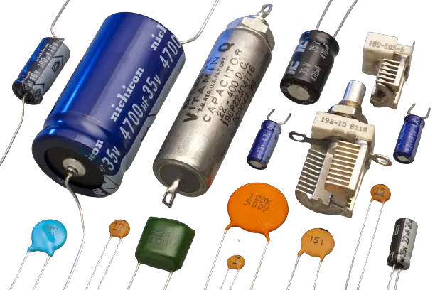
Capacitor types
Capacitor types, Image Source – Eric Schrader from San Francisco, CA, United States, Capacitors (7189597135)CC BY-SA 2.0

Theory of Operation

As mentioned earlier, a capacitor has two conductors separated by a dielectric medium. A capacitor works on the principle of Coulomb’s Law. Coulomb’s law states that –

Thus, a charge on one conductor will generate the force on the other conductor’s carrier, which further attracts opposite polarity charges and ripples the same type of charges. That is how an opposite polarity charge is induced on the other conductor’s surface.

Both the conductors hold an equal amount of charges, and the dielectric material develops the electric field.

Capacitance and Units of capacitance:

The capacitance of a standard capacitor is defined as the charge’s ratio to the conductor to the conductors’ voltage.

C = Q / V

C is the capacitance, Q is the charge on each conductor’s surface, and V is the voltage between two conductors.

The S.I unit of capacitance is given by – Farad(F).

One Farad capacitance is defined as the amount of capacitance a capacitor can generate if one coulomb of charge is applied to each conductor having one volt of voltage.

In practical devices, Capacitance is given by –

C = dQ / dV

* Most of the capacitors available in the market have capacitance rang in micro-farad.

A capacitor may behave differently at different times if it is placed in an active electrical circuit. Its behavior can be characterized by a long time limit and a short time limit.

Long time equivalence of a capacitor acts like an open circuit configuration (no current passes).

The short time equivalent of capacitors act like a short-circuit configuration.

V (t) = Q (t) / C = (1/C) * [ ∫t0t I (τ) dτ ] + V (t0)

Taking the derivatives, we get –

I (t) = dQ (t) / dt = C * [ dV(t) / dt ]

Symbol of Capacitor

There are different kinds of capacitor available. Different types of symbols are also there to represent them. Some of them are represented below using the diagrams. They are very useful to describe the circuit.

Capacitor types: Symbol
Different symbols to represent capacitor

A capacitor in a DC Circuit

Let us discuss a DC circuit where a capacitor and a resistor are kept in series with a constant voltage source – V0.

Let’s assume the capacitor was previously uncharged, and the opened switch is closed at time t0.

From Kirchhoff’s Voltage Law, we can write –

Vo = VR (t) + VC (t)

VR (t) is the voltage across resistor ‘R’ at time instant ‘t,’ and VC (t) is the measured voltage across the circuit’s capacitor at time instant t.

Vo = i (t) * R + (1/C) * [  ∫t0 t I(τ) dτ ]

Taking derivative on both sides, we get –

RC * [ di (t) / dt] + i(t) = 0

At time t, let say tis zero. The voltage of the resistor is Vo and of the capacitor is zero.

At that time, current would be – Io = Vo / R. Now solving the differential equations –

I (t) = (Vo /R) * e (-t / τ0)

V (t) = Vo (1 – e (-t / τ0))

τ0 = RC.

It refers to as the “Time constant” of the circuitry.

A capacitor in an AC Circuit

In an AC circuit, the capacitor produces impedance, which is the vector sum of resistance and reactance. Capacitor’s impedances and reactance is given by the following expressions.

Reactance = X = – 1 / ωC = – 1 / 2πfC

Impedance = Z = 1/ jωC = – j / ωC = –j / 2πfC

Here ω is the angular frequency; j is the imaginary unit.

The impedance depends inversely on capacitance. Increasing the capacitance and frequency causes a decrease in impedance and vice-versa.

Q factor:

Q Factor or Quality Factor of a capacitor is defined as the ratio of reactance to its resistance. The q factor is a measure of efficiency. The formula can be written as –

Q = Xc / R = 1 / ωCR

ω is the angular frequency, C is the capacitance of the capacitor, Xc is the reactance, and R is the equivalent resistance.

Capacitor in Series

The diagram represents the capacitors in the series connection. It shows that the separation distance is added up instead of the plate area. The series of the capacitance acts as a capacitor less than any of its components.

images removebg preview
Series connection of capacitors

The equivalent capacitance of the given connection, is –

1/Ceq = ∑ 1 / Ci = 1 / C1 + 1 / C2 + … + 1 / Cn

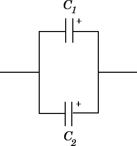
Capacitors in Parallel

The diagram represents the capacitors in parallel connection. An equal amount of voltage is applied to every capacitor. Here the capacitances of the capacitors are added up. The connection of the capacitance acts as an adder.

Cap par
Parallel connections of capacitors

The equivalent capacitance is –

Ceq = ∑ Ci = C1 + C2 + … + Cn

Capacitor Types

There is an enormous number of capacitor types, available in the market based on numerous classification parameters. Type of the dielectric material, the device packaging, and the plates’ structure are some of the determining factors to classify capacitor types.

Dielectric Material

Almost every capacitor types have a dielectric substance. Dielectric substances are placed in between two conductors, the charge capacity can be increased. It is best to have a high permittivity material or high breakdown voltage as a dielectric substance.

There are various dielectric materials available like – paper, plastic, mica, ceramic, glass, air, etc.

Based on dielectric materials, some capacitor types are –

There are also other types, some capacitor types are –

  • Voltage-dependent Capacitor
  • Frequency-dependent Capacitor
  • Parallel Plate Capacitor
  • Decoupling Capacitor

Applications of Capacitors

Capacitors are one of the essential devices which are required for almost every electrical circuit. It has numerous applications in various fields. Some of the most important are – 

Energy Storage

A capacitor has the property of charging and discharging. It can store energy when it is disconnected from the charging source. Using this property, capacitors can be used as a battery or rechargeable battery.

Super-capacitors can accept and deliver charges faster than typical batteries and tolerate a more significant number of charging and discharging cycles than a standard rechargeable battery. But it is more extensive.

The quantity of charge stored in the dielectric layer is equal to or greater than the charge stockpiled in a plate of capacitor.

Pulsed power

Capacitors are used in pulsed power applications. Mainly groups of large, primarily constructed, high voltage, and low inductance capacitors are used here.

Banks of capacitors are also used in power supplies to produce smooth outputs in half-wave or full-wave rectifier. Reservoir capacitors can be used for charging up pump circuits.

Industrial Use

This helps to shunt away and hide fluctuations of current from the primary source to ensure a clean power supply for the control circuits. Audio circuits also use several capacitors.

Signal Coupling and Decoupling

Capacitors pass the AC signal but block the DC signals. That’s why capacitors are used in separating AC circuits. The process is recognized as – AC coupling or ‘capacitive coupling.’

A decoupling capacitor safeguards one area of the circuitry from other. They are used in power supply grounds. These are also known as a Bypass capacitor. Decoupling capacitors has applications in the biasing of transistors.

Memory

Dynamic digital memories for binary computers can be made using capacitors.

50 MCQs with Answer Capacitors. Click Here!

Photo Detector:Features,Types,Advantages,7 Applications

DG 1 4

Contents of Photo diode detector

In this article we will discuss about photo diode detector as follows:

  • Definition of a photodetector
  • Different types
  • Circuit Diagram
  • Applications
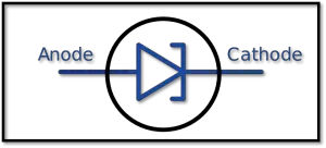
  • What is a Photodiode
  • Features of a photodiode
  • Working principle
  • Avalanche photodiode
  • Circuit Diagram
  • Applications
  • Advantages & disadvantages
  • Phototransistor vs. photodiode

What is a Photo Detector?

Definition of a Photo Detector:

“Photodetectors are important elements, possess the ability to transform light into electrical signals.”

Photodetectors are important elements useful in image processing, optical communication, security, and night vision and motion detection.”

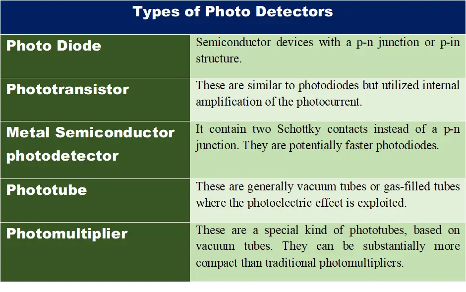
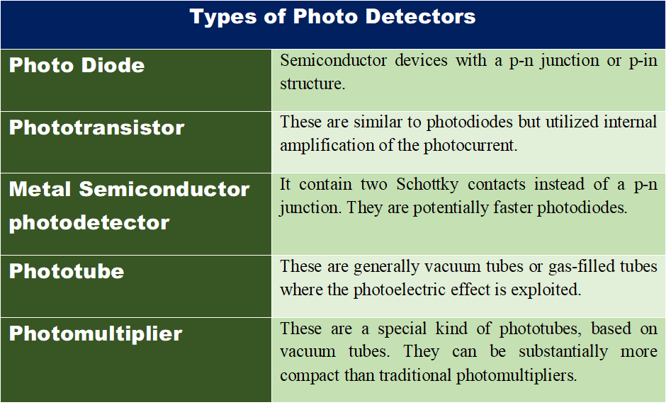
Types of Photo Detectors:

Photo Detector Types

Important Applications of Photo Detectors:

  • Photo Detectors can be employed for properties like optical power, luminous flux measurements.
  • These are used in various types of optical-sensor and microscope design.
  • Photo detectors are essential for laser rangefinders.
  • Fast photodetectors are commonly utilized in optical-fiber communication, frequency metrology etc.

What is a Photo Diode?

Definition of a photodiode:

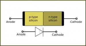
“A photodiode is basically a typically p-n junction diode.

When a photon strikes the diode, it will excite electron and generates a moveable electron and a positive charge hole. The absorption happens in the junction’s depletion area, the carrier will removed from the junction by the depletion region’s built-in potential.

How does a photodiode work?

Working Principle of photodiode:

A photodiode is a p-n junction or a P-I-N configuration. If a photon strikes the diode, it produces the electron and a positively charged hole. When there’s any absorption happens in the juncture’s depletion area, these carriers have been trapped in the juncture from the built-in area of this depletion region that created a photocurrent.

Photodiodes are widely used under inverse biasing or without biasing. The light or photon can drive a current across this circuitry, which gives to the forward bias, which subsequently causes ‘Dark current’ from the reverse direction to the photocurrent. This is referred to as the natural effect and can be the foundation of solar cell design. A solar panel is just a combination of multiple effectual photodiodes.

Reverse bias produce minor current along exactly identical direction. Apart from that, the photodiode exhibits less noise.

Avalanche photodiodes have a similar prearrangement, but it’s normally operated with a greater reverse biasing. This enables every single photo-generated provider to be multiplied with avalanche breakdown, leading to photodiode’s internal effects and improves the device’s overall responsivity.

Materials for a photo diode:

Material used in photodiode:

  • Silicon
  • Germanium
  • Lead Sulfide

The materials used for the construction of photodiode is important to describing its properties because only photons with appropriate energy can excite electrons in bandgap and able to produce substantial photocurrents.

It is important to remember that, silicon-based photodiode have greater band-gap and because of this it is capable to produce less noise than germanium-based photodiodes.

Since transistors and ICs are prepared by semiconductor material too and comprise p-n junctions, may act like a photodiode. This is not the accepted, an opaque housing is mandatory to remove this effect. Though these is not entirely opaque towards high energy radiations, may still cause ICs to malfunction for induced photocurrent.

Applications of a Photo Diode:

  • Photodiodes are used in consumer electronic i.e., CD players, fire and smoke detectors, remote controls, lighting etc.
  • These are also employed in various medical applications, detector and high-energy physics etc.

Advantages and Disadvantages of a Photo Diode:

ADVANTAGES-

  • Low noise
  • Low cost
  • Compact and lightweight.
  • Long Lifetime
  • No high voltage is required.
  • High quantum efficiency.

DISADVANTAGES-

  • Small area
  • No internal gain
  • Much lower sensitivity
  • Response time is slower.

What are the characteristics of a Photo Diode?

There are two types of characteristics of photo diode

  • Electrical Characteristics
  • Optical Characteristics

Electrical Characteristics of Photo Diode:

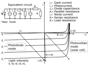
Photodiode operation
Equivalent circuit of silicon photodiode, Image Credit – Kennlinie_Photodiode_1.png: Gregor Hess (Ghe42) derivative work: Materialscientist (talk), Photodiode operationCC BY-SA 3.0

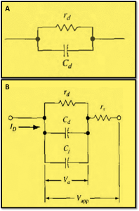
SHUNT RESISTANCE, RSH

Shunt Resistance (RSH) is used to estimate the thermal noise when no reverse bias is applied. It’s the ratio of voltage to current.

It is computed from the slope of the photodiode’s V-I curve at the origin.

SERIES RESISTANCE

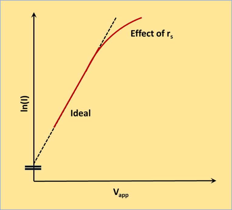
Series resistance is give by Rs and it comes from the resistances of silicon. The expression is given by the following equation –

3

JUNCTION CAPACITANCE, (Cj)

Junction Capacitance (Cj) is the capacitance of the diode at a given reverse bias.

The junction capacitance is proportionate to the diffusion area and inversely proportionate to the width of depletion area.

4

RISE AND FALL TIME ( tr , tf )

The time taken to reach Ninety percent from ten percent is known as Rise Time and the time taken to fall from Ninety percent to Ten percent is known as Fall time. This parameter commonly expressed in frequency response of 3dB decay as follows.

                                tr=0.35/f3dB

BREAKDOWN VOLTAGE (VBR)

It is the max negative voltage which can be applied to the diode terminal.

NOISE EQUIVALENT POWER (NEP)

The photon intensity is prerequisite to equivalent the noise at a specified reverse biasing. It is a measurement of NEP.

RESPONSE TIME (tr)

It is defined by the time required for a diode to respond a step input in light at a specified reverse biasing mode of operation.

Short circuit current (ISC):

With the diode pins shorted, the current that flows at a given light intensity.

Optical Characteristics of Photo Diode:

Response silicon photodiode
Image Credit: KaiMartinResponse silicon photodiodeCC BY-SA 3.0

QUANTUM EFFICIENCY, QE

QE is extensively recognized as the percentage of the incident photons that contribute to the photocurrent.

                               QE=R obs/R Id (100%)

RESPONSIVITY, R

The responsivity of a silicon photodiode is the measurement of the sensitivity to light. It is given by the ratio of Ip to the coming power of light (P) for the given wavelength.

                              R=IP/P at specific wavelength

NON-UNIFORMITY

It is well-defined as the variations of responsivity witnessed over the active photodiode surface area with a trivial spots of light.

NON-LINEARITY

A silicon photodiode characteristic is linear in nature though minor change in current regulates photocurrent linearity.

Noises in a Photo Diode:

In a photodiode, two types of noises are introduced; they are

  • Shot Noise
  • Johnson Noise.

Shot Noise

It is expressed by the following equation.

6

Thermal Noise or Johnson Noise

The photodetector may produce Johnson noise because of the thermal generation of carrier. The magnitude of this generated current noise is:

7

Hence, the total noise is,

8

Explain Avalanche and Zener Mechanisms:

Avalanche breakdown happens only at the higher voltages. Assume the electric field (E) in the transition region is enormous. Then, an e incoming from the P side may get accelerated with kinetic energy to collide with the lattice and produce ionization. The interactions will create carrier multiplication; the original electron and generated electron are swept to the N side, and the create hole is flounced to the P. This process is Avalanche since each incoming carrier be able to initiate the large number of carriers.

Zener effect happens once tunneling of electrons take place from the P-side valance band to N-side conduction band, may causes reverse current flow from N to P terminal. Basic inevitabilities for tunneling current are a large number of electrons that are detached from a substantial quantity of unoccupied state by a tinny barrier. Since the tunneling probability be governed by the barrier width, doping must be great.

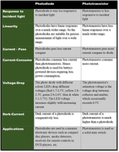
Compare between Photo Transistor and Photo Diode:

9

For more Electronics related article click here

Schottky Diode:Circuits, Important Characteristics,7 Uses

DG 1 3 300x136 1

CONTENTS

  • What is a tunnel diode
  • Tunnelling
  • V-I characteristics
  • Circuit diagram
  • Symbol
  • Applications
  • What is Schottky diode
  • V-I characteristics
  • Circuit diagram & symbol
  • Applications

What is a Tunnel Diode?

Definition of a Tunnel Diode:

“A tunnel diode is a type of semiconductor diode that has effectively negative resistance due to the quantum mechanical consequence known as ‘tunnelling effect.”

The depletion layer constitutes by a potential barrier at the junction. The potential barrier usually obstructs the flow of carriers from one to other side of the junction. If the concentration of impurity is significantly increased the device characteristics gets completely changed. A new diode by Esaki, gave the correct theoretical explanation for diode’s volt-ampere characteristic.

What is tunneling effect in semiconductors?

The Tunneling Effect or Tunneling Phenomenon:

“Tunneling is a purely quantum-mechanical procedure by which a microscopic particle can infiltrate a potential barrier even when the energy of the incident particle is lesser than the potential barrier.”

The width-size of the junction barrier inversely proportional to the square root of impurity concentration. This quantum mechanical behaviour is termed as ‘tunnelling’, and these p-n junction devices with high impurity concentration are called tunnel diodes.

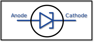
Symbol of a Tunnel Diode:     

DG 1 3
Symbol of a Tunnel Diode

Characteristic of Tunnel Diode:

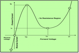
DG 2 3

A tunnel diode is a great conductor in the opposite direction. Also the resistance is less for little forward voltage. In the current IP known as peak current is corresponding to the voltage VP, the change in current to voltage (dI/dV) ratio stays 0. The tunnel diode displays a negative resistance characteristic involving the peak current IP and minimal value IV known as the valley current.

In the valley voltage VV, where I=IV, the conductance is ‘0’ and further than this point, the resistance gets positive. For the peak forward voltage VP, the current again touches the IP for more applied voltages the current can increases more.

 For this characteristics, the tunnel diode can be utilized in multiple device such as pulse and digital applications.

DG 3 3

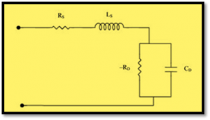
The negative resistance -RD has a minimum between IV and IP point. The series resistance is commonly termed as ohmic resistance (RS). The series inductance (LS) be influenced by the terminal length and the geometry. The junction capacitance CD depends upon the bias and usually is measured at the valley point. Switching times of the order of a nanosecond are in practical application, and switching times as low as 50 pico-seconds have been achieved.

Materials of a Tunnel Diode:

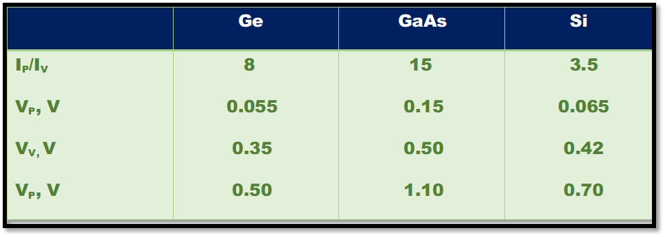
The Most Economical Commercially accessible tunnel diodes are created from Germanium and Gallium Arsenide semiconductors. It’s Hard to produce a metal tunnel diode using a high ratio of IP/IV or by the peak-to-valley current.

Typical Tunnel diode parameters

DG 4 2

From the above table, we can summarize the important static characteristics of these devices. The voltage values in the table are determined principally by the particular semiconductor used and are almost independent of the current rating. The peak current (IP) is measured by the impurity concentration and the area of junction.

What are the advantages & disadvantages of Tunnel Diode?

Advantages of tunnel diodes are

  • low noise
  • Simplicity.
  • higher speed of operation
  • Resistance to extreme environments.
  • Less power requirement.
  • Comparatively less expensive.

Disadvantages of Tunnel diode are

  • Tunnel Diodes are two-terminal devices, so no isolation between output and input. Sometimes, it could lead to serious circuit-design difficulties.
  • Low output-voltage swing obtained.

What is Schottky Barrier Diode?

Among the earliest practical semiconductor apparatus used in the early 1900s was that the metal-semiconductor diode. The diode, also referred to as a point contact diode, was created by attaching a metallic part into a bare semiconductor surface. These metallic semiconductor diodes weren’t readily duplicated or automatically reliable and were substituted by the p-n intersection. But, semiconductor and vacuum technologies is currently utilized to manufacture reproducible and reliable metal.

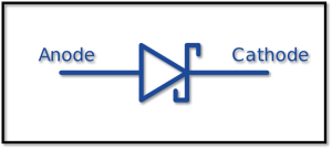
Symbol of Schottky Diode:

Symbol of Schottky Diode

Qualitative Properties of Schottky Barrier Diode:

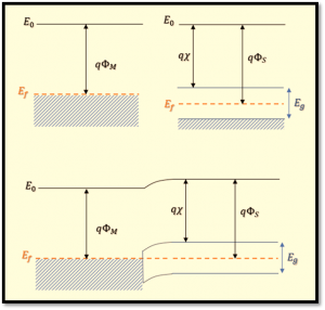
The Metal and semiconductor band diagrams when separated (top) and when in contact (bottom).

The perfect energy band diagram for a specific metal and n-type semiconductor prior to constructing contact is revealed. The vacuum level is used as a benchmark level. The parameter Øm is that the metal work function, ØS is your semiconductor work function and X is popularly referred to as the electron affinity. As a way for fermi level to develop into a continuous throughout the system in thermal stability, electrons in the semiconductor flow in the lower energy states from the alloy. Positively charged donor atoms stay in the semiconductor developing a space charge region.

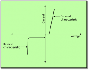
Voltage-Current (V-I) characteristic of Schottky Diode:

DG 8

The general shape of the metal semiconductor Schottky diode I-V characteristics are similar to a standard p-n junction diode.

P-N junction diode VS Schottky Diode:

ParameterPN JUNCTION DIODESCHOTTKY DIODE
PolarityIt is a Bipolar device  It is a Unipolar device
JunctionIt had Semiconductor to semiconductor junction.It has Semiconductor to metal junction formation
Voltage dropLarge forward voltage dropLower forward voltage drop
State lossOn state losses will be moreLow on state losses
Suitability Suitable for low frequency applicationsSuitable for high frequency switching applications

Applications of Schottky Diode:

  • The Schottky Diode utilized as rectifiers in switched mode power supplies (SMPS)
  • Schottky Diodes are in different solar cell applications.
  • They are used in different logic gate implementations
  • Schottky Diode can be used for AC to DC converter circuit.
  • In different detector applications they are also employed.

To know more about diodes click here

Digital To Analog Converter (DAC): Types, Working 5 Uses

Screenshot 2021 05 22 182437

Contents

·       Digital-to-analog Converter (DAC)

·       Working of a digital to analog converter

·       Electrical Symbol of digital-to-analog converter

·       Types of digital-to-analog converter

·       Applications of digital-to-analog converter

·       Advantages and Disadvantages of Digital to Analog Converter (DAC)

Digital to Analog Converter (DAC)

A digital to analog converter is an electronic device that does a conversion operation. As the name suggests, it converts a digital input signal into an analog output signal. Digital signals such as digitized music can be converted into analog sounds using a digital to analog converter. It is one of the types of data converters.

A digital to analog converter is also known as DAC, d to a converter, dac converter, D / A converter, etc. An analog to digital converter (ADC) does the reverse operation.  A DAC is required almost every time in the circuit whenever there is a need for ADC.

Know about Analog to digital converter!

Working of a digital to analog converter

A digital to analog converter is an equipment working for digital to analog conversion. A digital signal is defined as the discrete in time and discrete in the amplitude signal. At the same time, an analog signal is defined as the time-continuous and continuous amplitude signal. A DAC covert a fixed-point binary number (abstract adequate precision number) into a physical measurement.

The transformation has several steps in it. A typical digital to analog converter converts abstract data into conceptual sequences of impulses. Then the series is processed using a reconstruction filter. 

A digital to analog converter works based on the Nyquist-Shannon sampling theorem. It states that – an input signal can be recovered from its sampled output if the sampling rate is twice greater than or equal to the highest frequency component present in the input signal.

There are several parameters to measure the performance of a digital to analog converter. The bandwidth of the output signal, the signal to noise ratio are some of the parameters.

Electrical Symbol of a DAC

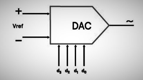
The below symbol represents a digital to analog converter.

Screenshot 2021 05 22 182437
Symbol of Digital to analog converter

Types of digital to analog converters

The conversion of digital input bits into analog signals can be achieved through different processes. Let’s discuss some of the types –

A. DAC using the weighted resistors method

Let’s get started with a 4-bit digital number. We will convert it into analog. Let the digital number – B3B2B1B0

Digital to Analog Converter
Binary Digital-to-Analog Conversion. Image Source – Giacomo Alessandroni creator QS:P170,Q100973368, Convertitore Digitale-Analogico a reti pesate a 4 bitCC BY-SA 4.0

The decimal equivalent will be – N = 23B3+22B2+21B2+20B0

Here B3 is the most significant digit (MSB) whereas, the B0 is the least significant digit (LSB). The circuit here operates to produce an analog output signal weighted according to the bit positions and add them together.

In the circuit, logic voltages, which represents the binary input, is applied to the corresponding resistors using switches. The resistors of the circuits (except feedback resistor Rf) are connected in a weighted way so that the successive ratio is 2. That is – R0 / R1 = R1 / R2 = R2 / R3 = 2. The resistors are also inversely proportional to their numerical significance of the appropriate binary bit.

When the binary bit is zero (0), the switch is turned ON and connected to the ground. If the binary bit is one (1), the controller is closed and connected to the reference voltage VR.

The current i which will be supplied to the non-inverting terminal is –

i = VR * ( B3 / R3 + B2 / R2 + B1 / R1 + B0 / R)

Substituting the values of R0, R1, R2, R3 we get –

i = (VR / R) * (23B3+22B2+21B2+20B0 )

Since G is virtual ground, the output voltage vo =

Vo = -i * Rf = – ( VR / R ) * Rf * ( 23B3+22B2+21B2+20B0 )

Now we can observe that the output voltage is proportionate to the numerical value of the binary digits.

The DAC accuracy depends on the resistor’s ratios and their ability to track each other when the temperature varies.

This type of digital to analog converters has some disadvantages. It requires a wide range of resistors to construct the converter if the binary input consists of a large number of bits. The R-2R ladder type converter overcomes this disadvantage.

B. R – 2R Ladder Type DAC

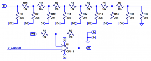
A ladder of resistances can convert a binary word into analog. This type of DACs is known as R – 2R Ladder-type converters.

r 2r ladder dac
R – 2 R Ladder Type Digital to analogue conversion. Image source – Wiki Analog

To understand the circuit’s operation, let us assume that the terminal B0 is connected to VR, and the rest of the terminals (B1, B2, B3) are connected to the ground.  The resulting figure is shown in the circuit –

We apply Thevenin’s theorem to the nodes a0, a1, a2, a3 concerning ground. We get the Thevenin’s equivalent circuit, which is further shown in the below course –

The equivalent source has a voltage of VR/16 in series with a resistance 3R.

Again, if the terminal B1 is connected to Vr and the terminals B0, B2, B3 are connected to the ground, then applying Thevenin’s theorem also, it can be shown that the source has a voltage VR /8 in series with a resistance 3R.

Similarly, when B2 is connected with VR and rest inputs are connected to the ground, we will find that the Thevenin’s equivalent circuit has a source voltage of VR / 4 in series with a resistance 3R.

Same for B3’s connection with VR. The equivalent circuit gives the source voltage as VR / 2 and the series resistance of 3R.

The current i obtained by the principle of superposition – 

i = ( Vr / 3R ) * ( B0/16 + B1/8 + B2/4 + B3/2 )

Since G is virtual ground, the output voltage vo =

Vo = -i * Rf = – ( VR / R ) * Rf * (B0 / 23 + B1 / 22 + B2 / 21 + B3 / 20 )

The equation comes as –

Vo = -i * Rf = – ( VR / 48R ) * Rf * ( 23B3+22B2+21B2+20B0 )

Here and now we can realize that the output voltage is proportionate to the numerical value of the binary digits. This circuit can easily convert large binary digits as it is easily extensible. All we need to add is additional switches and extra resistors for the ladder.

One of the vital features of a digital to analog converter is that the circuit’s smallest change defines its resolution.

Applications of digital to analog converter

The modern era has a high demand for digitized data. That is why there is an increasing demand for an analog to digital converter. But we have to keep in mind that we use analog signals in our day-to-day life, and the world is analog. So, whenever we need an analog to digital converter, we need a digital to analog converter. Both DACs and ADCs have contributed most to the digital revolution.

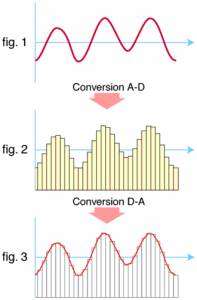
330px Conversion AD DA
A general process of DAC and ADC. Image Source – MegodenasConversion AD DA, marked as public domain, more details on Wikimedia Commons

Let us take a real-world example to understand their need. Consider a telephone call. At first, the caller starts speaking. The speech is an analog signal, which is changed into a digital signal using an analog to digital converter or ADC. When the digitized signal is transported to the receiver’s end, it again needs to be converted into an analog signal; otherwise, the receiver will not understand the sent data. Here a digital to analog converter serves the purpose.

Audio Processing:

Music and other audios are stored in digitized format in today’s era of digitalization. When we need to hear them in speakers or headphones, then the digitized form must be converted into an analog signal. That is why DACs are found in every device which can play music like – MP3 Music player, DVD player, CD player, Laptops, Mobile Phones, etc.

High-end hi-fi systems use specialized standalone DACs. Similar DACs are found in modern digital speakers such as USB speakers, sound cards, etc.

In voice over IP communications, the source is digitized. Thus a DAC is needed to reconstruct the digitized part into an analog signal.

Video Encoding:

The video encoder system processes a video signal and sends digital signals to ICs.

Digital Display:

The graphic controller typically uses a lookup table to generate signals sent to analog outputs such as RGB signals to drive the display.

Calibration:

A digital to analog converter can provide calibration of dynamic types to increase the test system’s accuracy.

Controlling Motor:

Digital to analog converters are also used in motor control devices where the voltage control signal is required.

DACs are also used in data distribution systems, digital potentiometer, software radio, and many other places.

Advantages and Disadvantages of Digital to Analog Converter (DAC)

Advantages of DAC

As mentioned earlier a digital to analog converter is as important as an Analofg to digital converter, it has too several points to discuss. Every electrical and electronic device has both its advantages and disadvantages. DACs are no exception. Some of its benefits are –

  • Large digital – binary inputs can be converted into its analog form easily.
  • One of the fastest methods of conversion.
  • Simple circuitries to implement.

Disadvantages of DAC

  • Circuits use expensive operational amplifiers.
  • Some errors like – gain error, offset error, Non-linearity is generally caused by resister employed in the circuit.
  • Power dissipation is high.

UFT Tutorial: Object Repository – Best Guide for UFT 14.x

UFT Object Repository Object Spy 157x300 1

Testing is now an important phase of the software development life cycle to secure the product’s quality. Also, without having testing, we can’t ensure the fulfillment of all the requirements. Here automation is playing an essential role in the testing cycle to reduce the efforts and time. In the market, there are multiple testing tools available to automate the testing process. The most used automation testing tool is UFT. 

In this topic, we are going to learn about the UFT Object Repository, descriptive programming approach and concept of virtual object in UFT, which are the most important features of UFT.

UFT Tutorial – Table of Content

UFT Tutorial #1: UFT Overview

UFT Tutorial #2: UFT Setup – Download, Install, License Configuration and ALM Connection

UFT Tutorial #3: UFT Object Repository

UFT Tutorial #4: UFT Actions & Function Library 

UFT Tutorial #5: UFT Parameterization 

UFT Tutorial #6: VB Scripting in UFT

UFT Tutorial #7: Step by Step Guide to Create Test Case in UFT

UFT Tutorial #8: Exception Handling in UFT

UFT Tutorial #9: Recording in UFT with Checkpoints & Dictionary Object 

UFT Tutorial #10: UFT Interview Questions and Answers 

 UFT Tutorial #3: UFT Object Repository

UFT Object Repository:

An object repository is the primary component of UFT as an automation test tool. It is the collection of test objects which are used to map the applications with the UFT test scripts. Basically, one or multiple properties that can uniquely represent any test objects of the application are stored in Object Repository. For example, name, id, inner text, these are the common properties used to represent any object. It follows the below properties to identify the field objects –

Mandatory property -> Assistive property -> Ordinal Identifier -> Smart Identification

Object Repository Classification: 

Two types of object repositories are available in UFT –

  • Local Object Repository
  • Shared Object Repository
UFT Object Repository - Local
Local Repository

Shared Object repository – An object repository that is located outside of the test case is known as a shared object repository. It can be shared across multiple actions or test scripts. We can build it with the help of the object repository manager. It’s used for reusability purposes. We can store it as a .tsr file in any location. This type of object repositories is mostly used for reusability purposes in Keyword or Hybrid test frameworks.

UFT Object Repository - Shared
Shared Repository

Guideline for Object Repository: 

  • The logical name of the objects in the repository should be given based on the application functionality.
  • Smart identification should be disabled to increase performance.
  • Object Repository size should not be big; descriptive programming can be partially used to reduce the size.
  • Handle dynamic objects through regular expressions or descriptive programming.
  • Use a shared object repository instead of a local.
  • Do not use multiple entries for the same object in Repository.

Different Options in Object Repository:

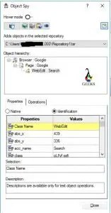
ObjectFinder – This is one of the most important and helpful features of UFT to analyze the test object. Through this option, we can view/analyze the different properties of test objects before adding them to Object Repository. It will help us to define the object identification approaches for test automation. Without object Finder, it is very difficult to define the descriptive programming approach.

UFT Object Repository - Object Spy
Object Finder

Add Object – It’s used to add any application object into the repository.

Update from the application – We can update any objects which are already added to the repository directly from the application through this option.

Highlight – Object can be highlighted in the application.

Locate in Repository – We can locate the actual object available in the repository from the application.

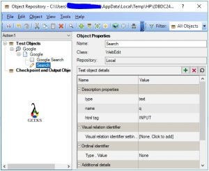
Object Properties section – Descriptive properties, ordinal identifier, and smart identification configuration can be view/ edit from this section.

UFT Object Hierarchy: The UFT test object hierarchy includes one or multiple levels of test objects. The highest level of the object may represent a window, dialog box, or browser type object, depending on the environment. For any web applications, three levels of object hierarchies are available – Browser, Page, and individual test object. So, the identification has been made sequentially from top to bottom.

Browser(“Test Browser”).Page(“Test Page”).Link(“test link”).Click

Object Identification Mechanism:

Objects from the repository can be identified based on the properties or behavior as appeared in the application. There are three different types of property options that are available to locate any object uniquely. Those are –

Descriptive Properties – Based on the application development, behavior or properties are defined in the application. It has two parts – Mandatory properties and assistive properties. Based on the uniqueness of the properties, UFT is able to identify the objects. First, the tool is to try to identify the Mandatory properties such as name, id, text, etc., which are defined during the application development, are used to identify the object. If any unique combination is not available, UFT is trying to identify the application with the help of some additional properties, which are referred to as assistive property. 

Ordinal Identifier – When the descriptive properties are not sufficient to identify any object uniquely, UFT is trying to define some additional properties based on the appearance of the objects in the application to identify. These properties are called an Ordinal Identifier. Three types of ordinal identifiers are available –

Index – it’s defined based on the position of the object in the application. Index value always starts from 0.

Location – it’s defined based on the location of the object in the application. The location value always starts from 0.

CreationTime – it’s defined based on the creation time of the object in the application. The value of CreationTime always starts at 0.

Smart Identification – When Descriptive properties and Ordinal Identifiers are failed to identify any object, some additional configuration/properties are used, which are predefined to identify the objects in this case. Smart Identification is the last option to identify the objects. It’s only applicable if we set the value as true. But this feature has slowed down the test execution. So, as best practices, in most cases, we need to disable these features.

UFT Object Repository - Property View
Property View of Repository

Step by step guide to add Objects:

  • Open the test application and move to the desire page/screen to add objects.
  • Open local object repository from UFT by clicking on the Object Repository icon or pressing “Ctrl+R” keys. In case of a shared repository, we can open it from “Resources-> Object Repository Manager.”
  • Click on the add object button(Green plus button) in the repository. Now the tool will allow us to select the object by clicking on the desired field in the application.
  • After the selection of an object, an intermediate “Object Selection – Add to Repository” popup will appear. Click on the OK button to add the object.
  • After adding the object, we can edit the properties or logical names based on the requirements.

Object Repository Manager:

Object repository manager is used to manage/ work with a shared repository. We can add, update, delete objects from the shared repository through the wizard. Navigation to open – Resources -> Object Repository Manager.

How to Create a Shared Object Repository:

The different approaches are – 

  • Create through Object Repository Manager – Open “Resources-> Object Repository Manager” and add objects from this window. After adding objects, we can save it as a .tsr file to create a shared object repository.
  • Converting Local Repository into Shared Repository – Exporting the local object repository (File -> Export Local Objects) into a shared object repository.
  • Drag Drop approach – Drag the objects from the Local Repository and drop them into a shared repository.

Associate Shared Object Repository in action: 

Two options are available –

  • In the Solution Explorer of UFT, right-click on the action name node and select the Associate Repository with Action.
  • In the Open Shared Repository dialog box, select the object repository and click Open.

Object Repository Comparision Tool:

This is used to compare two shared repositories and identify the mismatches. 

  • This tool can be opened from “Object Repository Manager” by the following path – “Tools-> Object repository Comparision Tool.”
  • Select both the shared repository and press on OK button.
  • Now comparision details will be available to analyse.
UFT Object Repository - Object Repository Comparision Tool
Object Repository Comparision Tool

Object Repository Merge Tool:

This is used to merge two shared repository into one. 

  • Merge tool can be opened from “Object Repository Manager” by the following path – “Tools-> Object repository Merge Tool.”
  • We need to select the primary and secondary repositories for merging. 
  • Now analyze the conflicts and save for merging both the repositories into the primary repository.
UFT Object Repository - Object Repository Merge Tool
Object Repository Merge Tool

Handling Dynamic Objects: 

Two options are available to handle dynamic objects – 

  • Descriptive programming approach – We later about descriptive programming in this article.
  • Regular Expression – It’s a series of characters that form a pattern/string which is used to identify the objects. We can define it by replacing the dynamic part of any properties with wild characters. Let see the below example – 

We have a dynamic link with text as – “Current date is 03-04-2000”. Here we can observe that in this link, the “Current date is “ part is constant by rest part is getting change every day. So we can use the either of below pattern while defining the objects in Object Repository –

Current date is .*” – Here ‘.*’ represent any string of any size.

Current date is \\d\\d-\\d\\d-\\d\\d\\d\\d” – Here ‘\\d’ can replace one numeric digit only.

Similarly, there are more regular expressions available. Please click here to see that.

Descriptive Programming:

Descriptive programming is an approach to define the description of the object during execution time. Through this approach, we can execute the test cases when the objects are not stored in the object repository. 

The purposes of using the Descriptive Programming approach are –

  • The test object is dynamic in nature.
  • To execute test cases without adding objects in Object Repository.
  • Execution performance may decreases if we use a big Object Repository. Descriptive programming can be used to avoid it.
  • ChildObjects are used to create a collection of objects which are matched based on the defined object descriptions. The parent objects proceed ChildObjects. Example – refer above example.

Working with descriptive Programming: 

There are two ways to develop test cases using descriptive programming –

1. Description Objects – Script is created using the Description object with the required properties. Example – Below descriptive programming approach is used to find the number of links available on a particular webpage.

UFT Object Repository - Descriptive Programming
Descriptive Programming

2. Description Strings – The Description of the object are passed as a string during the test case creation. Example –

                               Browser("MyApp").Page("MyApp").Link("text:=login","type:=Link").Click

Comparision Study between Object Repository and Descriptive Programming:

Object RepositoryDescriptive Programming
Object need to be added here.No need to add object in OR.
Difficult to handle dynamic objects.Easy to handle dynamic objects.
Reduce the performance of the execution.Increase the performance of the execution.
Object need to be defined prior to execution.Objects are defined during execution.

Virtual Object in UFT:

Sometimes, we have observed that objects in test applications are not recognized by the UFT for automation. Instead of that, the entire region identified as standard window objects. To handle this kind of scenario, UFT provides a feature as a virtual object to define those unrecognized objects as Button, link, textbox, etc., based on their behavior.

We can open the virtual object creation wizard from the path – “Tools-> Virtual Object->New Virtual Object.” By following the step by instruction from this wizard, we can define the Virtual Objects.

Limitations of Virtual Object are –

  • UFT is not able to record the virtual objects.
  • It’s not controlled by Object Repository.
  • Checkpoints can not be added here.
  • Object Finder can not inspect the virtual objects.
  • Execution may fail if the screen resolution has been changed.

Creation of Virtual Object in UFT:

1. Open Virtual Object Manager from navigation “Tools-> Virtual Object” and click on New button.

2. Click on Next from “Welcome to Virtual Object Manager” screen.

New Virtual Object Screen 1
New Virtual Object in UFT – Screen 1

3. Select class and click Next from “Map to a Standard Class” screen.

New Virtual Object Screen 2
New Virtual Object in UFT – Screen 2

4. Now mark the test object from application using mouse and click on next.

New Virtual Object Screen 3
New Virtual Object in UFT – Screen 3

5. Now configure the object and click next.

New Virtual Object Screen 4
New Virtual Object in UFT – Screen 4

6. Now click on Finish to save virtual Object.

New Virtual Object Screen 5
New Virtual Object in UFT – Screen 5

Conclusion:

In this article about UFT Object Repository, we have learned about how to identify objects from the application under test and the classification. Click here to understand more from the Microfocus support portal. Also, if you want to prepare for UFT Interview Questions, please click here.

Analog To Digital Converter:Working,Types,7 Applications

ADC Symbol 300x95 1

Content

·       Analog to digital converter (ADC)

·       Working Principle of an analog to digital converter

·       Electrical Symbol of analog to digital converter

·       Types of analog-to-digital converter & Explanations

·       Applications of analog to digital converter

·       Testing of an analog-to-digital converter

·       An ADC IC

Definition & Overview of Analog-to-digital Converter

An analog to digital converter is an electronic device. As the name predicts, the supplied analog signal is converted into a digital signal which is produced at output. Analog signals such as voice recorded by a microphone can be converted into a digital signal using an analog-to-digital converter. 

An analog to digital converter is also known as ADC and A to D converter, etc.

Working of an Analog to digital converter

An analog signal is defined as the time-continuous and continuous-amplitude signal. At the same time, a digital signal is defined as the discrete-time and discrete-amplitude signal. An analog signal is converted into a digital signal with the help of an analog-to-digital converter. The transformation has several steps, like sampling, quantization, and others. The process is not continuous; instead, it is periodic and limits the input signal’s allowable bandwidth.

An analog-to-digital converter works based on the Nyquist-Shannon Sampling Theorem. It states that – an input signal can be recovered from its sampled output if the sampling rate is twice greater than or equal to the highest frequency component present in the input signal.

There are several parameters to measure the performance of an analog to digital converter. The bandwidth of the output signal, the signal to noise ratio are some of the parameters.

Electrical Symbol of an ADC

The below symbol represents an Analog to digital converter (ADC).

Analog to digital converter symbol

Types of Analog to digital converters

The conversion of input analog signals into digital signals can be achieved through different processes. Let’s discuss some of the types in detail

A. Flash ADC

Flash ADC is known as direct-conversion type’s analog to digital converter. It is one of the fastest types of analog-to-digital converters. It comprises a series of comparators with the inverting terminals connected to a voltage divider ladder and the non-inverting terminals connected to the analog input signal.

As the circuit shows, a ladder of well-matched resistors is connected with a reference or threshold voltage. A comparator is used at each tap of the resistors’ ladder. Then there is an amplification stage, and after that, the code is generated as binary values (0 and 1). An amplifier is also used. The amplifier amplifies the voltage difference from the comparators and also suppresses the comparator offset.

If the measured voltage is above the threshold voltage, then the binary output will be one, and if the measured voltage is less than the binary work will be 0.

Recently improved ADCs are modified with digital error corrections systems, offset calibrations, and also, they are a smaller size. ADCs are now available in integrated circuits (ICs).

This type of analog-to-digital converters has a high sampling rate. Thus, it has applications in high-frequency devices. Detection using radars, wide-band radios, various testing equipment are some of them. NAND Flash memory also uses flash type analog-to-digital converters to store up to 3 bits in a cell.

Flash type ADCs are fastest in operation speed, simple in circuitries, and conversion coincides instead of sequentially. Though, these requires considerable numbers of comparisons than different types of ADCs.

Flash ADC

Flash Type ADC
Image Credit: Jon Guerber, Flash ADCCC BY 3.0

B. Successive Approximation type ADC

Successive approximation type ADC is another type of analog-to-digital converter which uses binary search through quantization levels before conversion into the digital domain.

The whole process is divided into different sub-processes. There is an ample and hold circuit, which takes the analog input, Vin. Then there is a comparator that compares the input analog voltage with the internal digital-to-analog converter. There is also a successive-approximation register (SAR), which takes input as clock pulse and comparator data.

The SAR is primarily initialized to make the MSB (most significant bit) as logic high or 1. This code is supplied to the digital-to-analog converter, which further provides the analog equivalent to the comparator circuit compared to the sampled analog input signal. If the voltage is more than the input voltage, then the comparator resets the bit. Else the bit is left as it is. After that, the next bit is set to a digital one, and the whole process is again done until every bit of the successive-approximation register is tested. The final output is the digital version of the analog input signal.

There are two types of successive-approximation types analog-to-digital converters available. They are – Counter type and Servo tracking type.

These types of ADCs give the most accurate results than other types of ADC.

SA ADC block diagram
Successive Approximation type ADC
Image Credit :White Flye, SA ADC block diagramCC BY-SA 2.5

C. Integrating type ADC

As the name implies, this type of ADCs converts continuous-time and continuous amplitude input analog signal into a digital signal using an integrator (an integrator) to apply an operational amplifier that takes a usual input signal and gives time-integrated output signal).

An unidentified analog input voltage is applied at the input terminal and allowed to ramp for a certain period, known as the run-up period. A pre-determined reference voltage of opposite polarity is then applied to the integrator circuit. That is also allowed to ramp until and unless the integrator gives the output as zero. This time is known as the run-down period.

The run-down time is generally measured in units of the ADC’s clock. So, longer integration time results in higher resolution. The speed of this type of converter can be improved by compromising with the solution.

As the speed and resolution are inversely proportional, this type of converters does not find digital signal processing or audio processing applications. Preferably, they are used in digital measurement meters (ammeters, voltmeters, etc.) and other instruments where high accuracy is crucial.

This type of ADCs has two kinds – charge balancing analog to digital converter and Dual-slope ADC.

D. Wilkinson ADC

– D. H. Wilkinson first designed this type of analog-to-digital converter in the year 1950.

At first, capacitor gets charged. A comparator checks this condition. After getting to that specified level, now the capacitor starts discharging linearly, producing a ramp signal. A gate pulse is also initiated in the meantime.  The gate pulse remains on for the rest of the time while the capacitor discharges. This gate pulse further operates a linear gate which further receives input from an oscillator clock of high-frequency. Now, when the gate pulse is ON, several clock pulses are being counted by the address register.

E. Time Stretch Analog to Digital Converter (TS – ADC):

This type of Analog-to-digital converter are functioned on a combined technology of electronics and other techs.

It can digitalize a very high bandwidth signal that cannot be done using an ordinary ADC. This is often termed as “Photonic Time Stretch Digitizer”.

It not only analog to digital but also used for high-throughput real-time equipment such as imaging and spectroscopy.

There are several other types of other analog-to-digital converters.

  • The Delta-encoded ADC
  • The Pipelined ADC,
  • The Sigma-delta ADC,
  • The Time-interleaved ADCs etc.

What is DAC? Know more about Digital to analog converter! Click to know!

Applications of ADC

The analog to digital converter is one of the most important electronic devices in this modern era. This is an era of digitalization, but our world is analog in real-time. Converting analog data in the digital domain is the need of this hour. That is why they are so important. Some of the significant applications of an ADC are – 

A. Digital signal processing

– Analog to digital converters are essential for editing, modifying, processing, storing, and transporting data from the analog field to the digital area. Microcontrollers, digital oscilloscopes, and critical software find applications in this domain. Devices like digital oscilloscopes can store waveforms for later use, whereas an analog oscilloscope cannot.

B. Microcontrollers

– Microcontrollers makes a device smart. At present, almost all microcontrollers have analog to digital converters inside them. The most common example may be the Arduino. (It is built on an ATMega328p microcontroller) The Arduino provides a useful function of ‘analogRead(),’ which takes analog input signals and returns digital data generated by the ADC.

C. Scientific Instruments

ADCs are useful for making various necessary electronics instruments and systems. Digital imaging for the digitization of pixels, radar technologies, and many remote sensing systems is an example. Devices like sensors produce an analog signal for measuring temperature, light intensity, light sensitivity, air humidity, air pressure, pH of a solution, etc. All these analog inputs are converted by ADC to generate a proportionate digital output.

D. Audio Processing:

-ADC has a vital application in the field of audio processing. The digitization of music enhances music quality. Analog voices are recorded via microphones. Then they are stored in digital platforms using an ADC. Many tunes recording studios record in PCM or DSD formats and then down sampled for digital audio productions. They are used for broadcast on televisions and radios.

Testing of an analog to digital converter

To test an analog-to-digital converter, first of all, we need an analog input voltage source and electronics equipment to send and control signals and receive the digital output data. Some of the ADCs also requires a source of reference signals. There are some parameters to test an ADC.

Some of them are –

  • Signal to noise ratio (SNR),
  • Total harmonic distortion (THD),
  • Integral nonlinearity (INL),
  • DC offset error,
  • DC gain error,
  • Power Dissipation, etc.

ADC IC

ADCs are commercially available as ICs in the market. Some of the commonly used ADC ICs are ADC0808, ADC0804, MPC3008, etc. They find applications in devices like Rasberry pi and other processors or digital electronics circuits where an ADC is needed.

To know more about electronics click here

PN Junction:Properties,Circuit,7 Important Applications

PN Junction Diode 300x161 1


C O N T E N T S

In this article we will learn about PN junction diode and it’s characteristics as follows:

  • What is PN junction diode ?
  • Definition of PN junction diode:
  • Working Principle of PN junction diode
  • Properties of PN junction diode
  • Circuit and symbol of PN junction diode
  • Equivalent Circuit of PN junction diode:
  • PN junction Current flows
  • Ideal current-voltage relationship
  • PN junction Characteristics
  • Diode quasi-fermi levels
  • Applications of PN junction Diode

What is a PN junction diode?

Definition of PN junction diode:

A pn junction diode is two-terminal or two-electrode semiconductor device.

“A diode is called as P-N junction diode if it is formed by P-type on one side and N-type on the supplementary one or reverse direction.”

The diode has to be in forward biased condition to permit the electric current flow. through it.

  • If a positive voltage is connected to the P terminals, the current then pass through from the P to N region as positive voltage helps to cross the depletion region. When we use a negative voltage is applied to the p-type, the depletion zone increases and prevents the current from flowing.

How does a PN junction Diode work?

PN junction diode
PN junction diode

Working Principle of PN junction diode:

In a PN junction Diode, we will consider the p-n junction with a forward-bias voltage employed. We can determine the current-voltage characteristics. The potential barrier of this p-n junction is reduced when a forward-bias voltage is applied to it. It will allow e- and hole to leak through the space charge region.

When holes begin passing through the p region throughout the space charge area, they get excess minority carrier namely, hole and extra minority carrier from drift, recombination and diffusion process.

Likewise, when electrons in the region initiate flowing through the space charge region to P.  They get surplus minority carrier electrons.

When semiconductor apparatus with p-n junctions are employed in linear amplifiers, as an instance, time-varying signs are overlaid on the dc currents and voltages. A tiny sinusoidal voltage apply to on a dc voltage applied across a p-n junction will initiate a small-signal current.

The proportion of the current to voltage generate the small-signal admittance of this p-n intersection. The admittance of a forward-biased p-n intersection includes both the conductance and capacitance parameters.

What is the PN junction current?

When a forward-biased voltage is applied to a p-n junction, a current gets generated in the device. That is known as P-N junction current.

Define the ideal current-voltage relationship:

DG 1 2

Ideal PN junction current:

The ideal current at a p-n intersection relies on the important components of the fourth principle mentioned previous section. The total current at the intersection is the summation of these electrons and hole currents, that stay steady through the depletion area.

The gradients from the minority carrier concentrations create diffusion currents, and because we’re considering that the electrical field to be ‘0’ at the space-charge edge, we can ignore drift current for minority in this approach.

Equivalent Circuit of PN junction diode:

The small-signal equivalent circuit of the forward-biased p-n junction is derived from an equation.

Y =gd+ Jωcd

DG 2 2
Equivalent Circuit of P-N junction diode

It is required to add the junction capacitance in parallel to the diffusion resistance (rd) and diffusion capacitance. The last element for the equivalent circuit is a series of resistance. The neutral n and p regions have a ‘C’ numbers pf resistances, so the actual p-n junction includes a series resistance which complete equivalent circuit is represented in above Figure.

The voltage through the actual junction is – Actual voltage (Va), and the total voltage applied to the p-n diode is specified by (Vapp) So the expression for the ideal condition as follows:

              V­app = Va+Irs

DG 3 2
Forward-biased I-V characteristics for p-n junction diode with the effect of series resistance

The above figure is V-I characteristics that reveals the impact of the series resistance. A voltage, that can be greater in general, is needed to find the exact same present value when a streak of immunity is included. In the majority of the diodes, the show resistance will probably be negligible.

In certain semiconductor apparatus with p-n junctions, but the series resistance will belong into some feedback loop.

Reverse Biased Recombination Current:

If a PN junction diode is in reverse biasing, It was learnt that mobile holes and electrons were wiped from the space-charge section. The negative signal explains a negative recombination rate; therefore, we’re actually generating electron-hole pairs inside the reverse-biased space charge region.

The recombination of excess holes and electrons at the procedure during the attempt to re-establish the thermal balance. Considering that the concentration of holes and electrons is essentially zero at the reverse-bias area, holes and electrons become generated through the trap level, which also attempts to revive the thermal balance.

Since the holes and electrons are generated, they are trapped from the space-charge area by the electrical field. The flow of charge is at the current direction of a reverse-biasing. This reverse-bias production current, which is principally a result of the creation of holes and electrons at the space-charge region, is added to the reverse-bias ideal saturation current.

Forward Biased Recombination Current:

For a reverse-biased PN junction, electrons and holes are cleared up mostly from the Space charge region. Under forward bias, however, electrons and holes are injected across the space charge region; during that some extra carrier charges may be at the space charge region.

There are certain possibility exists that some of these electrons and holes will recombine also during that time.

Diode quasi-fermi levels

DG 6 1
Quasi-fermi levels of Diode
Image Credit: Brews ohareDiode quasi-fermi levelsCC BY-SA 3.0

What are the uses of PN junction, diode?

Important applications of PN junction diode:

The critical applications of PN junction diodes are:

  • PN junction diode can be used as photodiodes.
  • PN junction diode can be used as solar cells.
  • The forward biased PN junction diode is used as LED.
  • PN junction diode used as rectifiers in voltage-controlled device in varactors.

To know more about diode click here