Topic of Discussion: CMOS Amplifier
- What is CMOS ?
- What is CMOS Amplifier ?
- Input Offset voltage
- Different parameters in CMOS amplifier
- Applications of CMOS Amplifier
What is CMOS ?
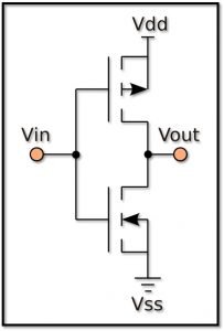
CMOS:

What is a CMOS Amplifier ?
CMOS Amplifier:
CMOS amplifiers (complementary metal–oxide–semiconductor amplifiers) are universal analog circuits utilized in personal computer, laptops, audiovisual device, mobilephones, cameras, communication systems, different biomedical applications, to many more other applications. In high performing CMOS amplifier circuitry, transistors are generaly used. Transistor not only utilzed to amplify the signals but those are also utilized as active load to attain high gain and output swing in comparison to resistive loading blocks.
The above figure shows a two stage CMOS Amplifier.
Some of the critical parameters which represents the amplifiers are – 1. Range of the supplied voltage, 2. Response to frequencies, 3. Response to the Noises, etc.
Input Voltage Range:
The range designates a “permissible” I/P voltage that will generate a linear, non-distorted O/P signal.
VDS>VGS – VT
VG is the input voltage, VD is VDD -VSAT for PMOS.
From the above explanation, the input voltage is able to swipe to some degree above the voltage VDD. The M15 and M16 are constructed to oppose to that current direction of M14. Nonetheless, VDM12 is not equal to VDM14.
Signal Path of CMOS Amplifier:
Signal-path represents the path through which the signal reaches to the output from the input. The signal path employed to investigate the freq-response, stability, and many more factors.
As the standard CS amplifier has high gain, the Miller effect will increase the total input capacitance. Any capacitance between output and input can be seen as capacitance at the input to the ground with the multiplication of (1 + Gain).
Load in CMOS Amplifier:
We can observe two varieties of active load in CMOS Amplifier: The diode connected MOS or current source MOS.
- It represents the output associated with a source of current. The current source acts as ‘Load’ for the output.
- By reason of Vgs of the active load is constant. Resistance value is r0 = 1/λId, where Id is drain current. The low frequency or direct current (DC) gain,
Av = gmn (roM16 // r0casp) gM17 (r0M18 // r0M17)
Typical load problem:
• Buffer configuration is a severe test for instability. It is found that a need of having a greater compensation capacitor for this purpose.
• It cannot drive a small load resistor.
CMOS Amplifier Parameters:
Input Offset:
The offset voltage is Vref – VI
The offset voltage of the amplifier has presented in above figure. This is measured from the disparities by taking considerations of paramter such as threshold voltage, load resistance, etc.
Common Mode Rejection Ratio (CMRR):
“CMRR is given by the ratio of the gain of the amplifier in differential mode to the gain of the amplifier in common mode.”
Power Supply Rejection Ratio(PSRR):
Power Supply Rejection Ratio or PSRR is given by the ratio of Output voltage to the input voltage. PSRR describe the noise rejection of CMOS amplifier. Typical method to improves the power supply rejection ratio is generally by by means of a cascode current source or sink (this is because of high output resistance value).
Slew Rate and Settling Rate:
- High slew rate
- Small compensation capacitorIncrease the operating current
Settling time is equivalent to Tsettling parameter and
Slew Rate = Vidmax
Noise:
For 1 μA, 7.8 × 10¹² electrons passing every second will generate a noise of 7800 Giga Hertz.
1. The higher input transistor is required to reduce the noise level.
2. Increase in operating current is also required.
3. White and short noise is mostly constant during the total operation
4. Flicker noise
Compensation in Amplifier:
Compensation is required to ensure stability in opamp. A CMOS Amplifier, loop-gain and phase are the prameter generally specify the Amplifier’s stability. The Op-Amp is generally constructed in a closed-looped for gain and phase analysis puropse. Suitable capacitance, resistance and biasing is also required for the compensation of amplifier.

Image Credit: Two-stage amplifiers-compensation-methods by Alireza1990polimi is licensed under CC BY-SA 4.0
Uses of CMOS Amplifier:
- This complementary metal–oxide–semiconductor amplifiers are utilized in personal different electronics consumer products such as computer, laptops, audiovisual device, mobile phones, cameras etc.
- These are one of the important component of telecom appliance
- Different biomedical applications utilized these type of amplifier nowadays. There are many more other applications of CMOS amplifier and list is increasing.
For more about MOSFET basics and others electronics related article click here
Read more about Log & Antilog Amplifier.

Hi, I am Soumali Bhattacharya. I have done Master’s in Electronics.
I am currently invested in the field of Electronics and communication.
My articles are focused on the major areas of core electronics in a very simple yet informative approach.
I am a vivid learner and try to keep myself updated with all the latest technologies in the field of Electronics domains.
Let’s connect through LinkedIn –