Power Transformer:Design,Rating,Losses,Efficiency,Uses

Pole transformer 2 300x200 1
  • Power transformer definition
  • Power transformer design
  • Power transformer diagram
  • Power transformer rating
  • Power transformer losses
  • Power transformer efficiency
  • Power transformer application ( in a substation)
  • Power transformer maintenance
  • Power transformer failure

Power transformer definition

A typical transformer can be defined as “A device that transfers electrical energy between electrical circuits.” It is a passive and static device. A power transformer is one of its kind. Power transformers are used to interface step down and step up voltages in the power distribution system. 

A typical power transformer has a life span of around 30 years.

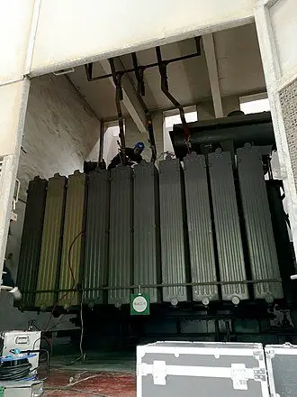
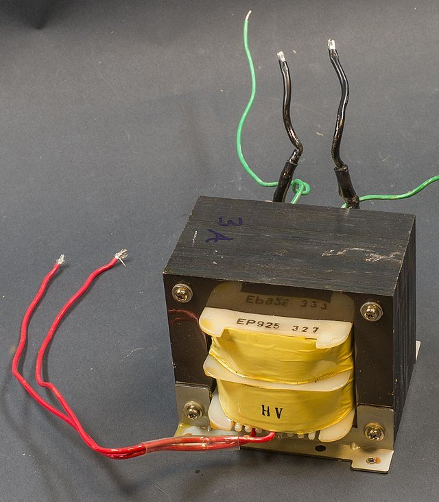
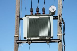
Pole transformer 2
A power transformer, Image Credit – ZngZngPole transformer 2CC BY-SA 4.0

Power transformer Design

A typical transformer consists of parts –

  • A. Metallic core
  • B. Two windings made up of coils

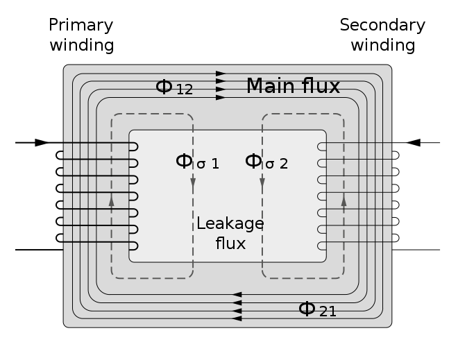
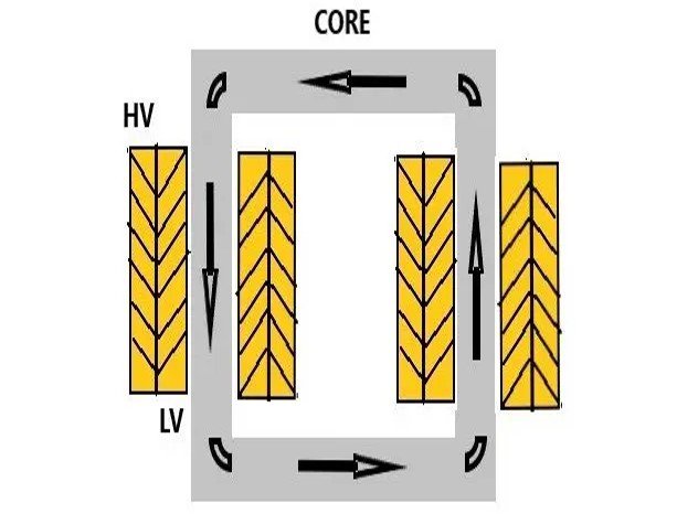
A power transformer has the same components as a normal one. Additionally, it has a cooling system and a metallic skeleton, which is laminated with sheets. Depending on the core structure, a power transformer may be either shell type or core type. This may also be three-phase or single phase-type. A three-phase can be made from three single-phase transformer.

Primary and secondary windings are wrapped using conductors either from inside or from outside the core. Single-phase and three-phase both the transformers need ‘bank’ to place the windings. If we use three single-phase transformers, then it is necessary to identify each bank isolated from others. If one of the banks fails, then also the transformer will ensure continuous service. But in the case of a single three-phase transformer, it won’t work if a bank fails.

All these settings with the core are kept inside a skeleton. The skeleton is absorbed inside a fire-protected oil. The oil both does the job of isolation and cooling. There is busing (isolators), which allows the conductor to do their job without interfering with the outer structure. Transformers need a cooling device too. A fan or some other process may serve the process.

Power transformer Diagram
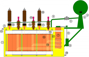
660px Vermogentransformator 1
Parts of power transformer, Find the details in source, Image Source – Fluppe37 at nl.wikipediaVermogentransformator 1CC BY-SA 3.0

Power transfer rating

Transformers are rated based on the power it can deliver to the load. If a transformer gives 5 volts and 4 amperes current as output, then the transformer’s rating will be 5*4 = 20-volt ampere. That’s why transformers are rated in Volt – Ampere (VA) or Kilovolt – Ampere (kVA). It usually work for higher voltages and are rated in kilovolt ampere.

A power transformer is a costly part of a distribution system. If the power rating isn’t done correctly, then the transformer may be burnt out. So, it is necessary to rate a power transformer accurately. The current value can be calculated using the diameter of the coil of the windings. The voltage can be calculated using the number of turns or using the turns ratio.

Power transformer losses

A power transformer suffers loss as it is not an ideal transformer. A transformer loss means loss of power. Losses of the transformer can be divided into four categories. They are –

  • A. Core Loss / Iron Loss (Hysteresis Loss & Eddy Current Loss)
  • B. Dielectric Loss
  • C. Copper loss or Ohmic Loss
  • D. Stray Loss

A. Core Loss / Iron Loss:

These losses are also termed as “No Load Losses”. This transformers suffer such losses whenever it is plugged in with power even it has no load connected with it on the secondary side. These types of losses are constant and do not fluctuate. Iron loss is also of two kind –

  • a. Hysteresis losses
  • b. Eddy current losses

a. Hysteresis losses:

  • An alternating magnetizing force occurs inside the core of the transformer. Due to the magnetizing leverage, a hysteresis loop traced out and power dissipated in the form of heat. Hysteresis losses cause a 50% to 80% no-load loss.

Ph = η * Bmax * n * f * V

Ph = Hysteresis Loss

η = Steinmetz hysteresis coefficient

Bmax = Maximum flux density

n = Steinmetz exponenet

f  = frequency of magnetic reversals per second

V = volume of magnetic material

b. Eddy Current Loss:

  • Eddy current loss occurs due to Faraday’s law of induction. An emf is induced in the core circuit due to the magnetic flux. This emf cause flow of current through the core structure as it is made up of iron. This current is known as Eddy Current. Eddy current is not useful for working in this circuit. So, the power loss due to this current is known as eddy current loss. Eddy current losses are accountable for 20% to 50% no-load loss.

The loss is given by –

Pe = Ke * Bmax2 * f * V * t2

Pe = Eddy Current loss

Ke = Eddy current constant

Bmax = Maximum flux density

= frequency of magnetic reversals per second

V = volume of magnetic material

t = magnetic thickness

B. Dielectric Losses:

  • Insulators placed inside transformers are the reason behind this loss. It is not a significant loss and contributes 1% of the total no-load losses.

C. Copper loss or Ohomic loss:

  • This type of loss in a power transformer can be called Load Losses as transformers suffer this type of loss due to short circuit conditions or when connected with the load. The resistance of the wire’s windings is the source of this loss. As most of the cables are made up of copper, the loss is named after that.

D. Stray Loss:

  • This loss occurs due to the leakage flux. The leakage flux depends on several parameters like – winding’s geometrical structure, the tank’s size, etc. Changing these parameters can also reduce loss. It is a negligible loss.

There are some other losses too. One of them is Auxiliary losses. The cooling system of the transformer causes this type of loss. Also, imbalanced and distorted power results in some extra losses.

Power Transformer Efficiency

The efficiency of an Electrical device is given as the ratio of output power to the input power.  It is given by – η.

η = Output / Input * 100%

In a practical scenario, a transformer has losses, as mentioned earlier. This loss is numerically equal to the difference between the Input power and Output power, that is –

Loss = Input Power – Output Power

Or, Output Power = Input Power – Loss

Now, efficiency can be written –

η = (Input Power-Loss) / Input Power * 100%

η = 1- (Loss / Input Power)  * 100%

It can also be written as –

η = (V2I2Cosϕ / ( V2I2Cosϕ+ Pi+ Pc ))* 100%

Where,

V2 = Secondary voltage

I2 = Secondary current

Cos ϕ = Power Factor

Pi = Iron Loss / Core Loss

Pc = Copper Loss

A large power transformer can achieve efficiency by up to 99.75%, and a small one can achieve efficiency by up to 97.50 %. If a power transformer’s efficiency stays in a range of 98 to 99.50%, it will be considered good.

The need for power is increasing by leaps and bound. In the case of the distribution of power, a power transformer is one of the essential tools needed. Though these are designed for higher efficiency, the need is high for more efficiency with a concern towards the environment and reduced usage of power. The reduction of losses is the way towards this goal.

Power transformer Application (Power transformer in a substation)
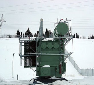
330px Transformer Limestone Generating Station 1
A power transformer in a substation, Image Source – Jasonbook99Transformer-Limestone-Generating-StationCC BY-SA 3.0

Transformers are one of the essential and most incredible innovations in the field of Electrical Engineering. Power transformers have the most use in the power distribution system. Some of the applications are –

  • Power transformers are used in power generation and distribution systems.
  • Power transformers are used in Sub-stations. A substation transforms higher electrically voltages to lower voltages, and a power transformer does this work. these are the most critical device of a power substation.
  • To reduce power losses in power transmission. Transformers help to minimize power, and thus electricity can be supplied throughout the areas.
  • To step up and step-down voltages as per the need.
  • Power transformers work continuously, ensuring supply for 24 * 7. Thus, when we need to do always, a transformer can be used.
  • These are also find application in Earthing transformers, isolation transformers.

Power transformer maintenance

Power transformers are expensive, bulky, and an essential part of a power distribution system. So, a transformer needs a high quality of maintenance. Maintenance can be two types – a daily basis and at the time of emergency. Regular maintenance is highly recommended for this type of transformer, which is placed in a substation. Some maintenance types are given below –

Regular Maintenance:

  1. Checking of oil level
  2. To keep the oil level at the desired level.
  3. To seal up leakage if any detected.
  4. To replace the silica gel if the colour changes to pink.

Monthly Maintenance:

  1. Oil level to avoid damage.
  2. To check up the bushings.
  3. Cleaning of the skeleton.

Half Yearly Maintenance:

  1. To check the IFT, DDA, flashpoints.
  2. To check acidity, water content, and dielectric strength.

Annual Maintenance:

  1. Check the condition of the oil—the situation in terms of moisture content and dielectric strength.
  2. To check up on all alarm and control switches.
  3. Measuring and checking the earthing connection.
  4. Checking of bushings and cleaning them up.
  5. To check a press release device.

Power transformer failure

A typical electrical transformer is quite complex in its circuitries. A power transformer is more complicated as it has some additional elements. A transformer fails by burning out or shut down of a transformer. A transformer’s failure may occur due to several reasons. Mechanical faults, periodic maintenance, natural calamity like lightning may lead a transformer to destruction.

  • Transformers generates heat during operation. If there are low-quality material for isolation, then the generated heat would lead towards burning.
  • Overloaded condition is another cause for transformers.
  • Old transformers can cause failure. Mechanical faults are prominent for old transformers.
  • If the oil’s moisture content fluctuates from the rated values, that may also lead to failure.

The power failure may be prevented by doing regular maintenance. Information based on previous failures also helps to detect signs of a power failure before the incident occurs.

To know more about transformer click here
9 Facts On JFET :Working,Features,Applications,Pros & Cons

Picture1 Symbol 300x190 1
  • What is JFET ?
  • Types of JFET
  • Characteristics of JFET
  • BJT vs FET
  • JFET vs MOSFET
  • Applications
  • Advantages & Disadvantages

In this article we will learn about the Field Effect Transistor or FET in details and one of its important type namely, Junction Field Effect Transistor (JFET) in detail.

Field Effect Transistor (FET):

In a field-effect transistor, only an electrical field is used to control the flow of current. FETs are unipolar transistors. Field Effect Transistor (FET) have three terminals, which are Source, Drain, and Gate.

Field Effect Transistor Types

There are two main types of field effect transistor,

  1. Junction Field Effect Transistor (JFET)
  2. Metal Oxide Semiconductor Field Effect Transistor (MOSFET) or Insulated-gate Field Effect Transistor or IGFET).

Features of Field Effect Transistor

  • Unipolar – In Field Effect Transistor, the conduction is happening either by hole or electron.
  • High input impedance − the Field Effect Transistor has high input impedance as input current in FET has flown due to the reverse biasing only.
  • Output impedance – FET’s Output impedance is very small.
  • Voltage-controlled device − Field Effect Transistor is called the voltage-controlled device as its output voltage is controlled by the gate input voltage only. 
  • Noise is low − The Noise of Field Effect Transistor is lower than in BJTs as in FET, no junctions present in the conduction path.
  • Gain – The Gain is characterized as trans-conductance in Field Effect Transistor.

Junction Field Effect Transistor

JFET is one of the simplest type of field effect transistor which have three terminal semiconductors.

Unlike PNP and NPN transistors, the three terminals of a Junction Field Effect Transistor are,

  1. Source
  2. Gate
  3. Drain

Junction Field Effect Transistor (JFET) working

JFET is a voltage-controlled device as it is controlled by use of a reverse bias voltage to the gate terminal. The channel gets drained and the electric current becomes switched off. A Junction Field Effect Transistor is usually said to be on when there is no voltage between the gate and the source pin.

Junction Field Effect Transistor (JFET) is usually two types as it is used n-type or p-type channel as per working. In the n-type, when the voltage source is connected to the gate is -ve with respect to the source, the current decreases. Correspondingly, when a JFET have a p-type channel, if a positive voltage is applied to the gate with respect to the source the current becomes reduced.

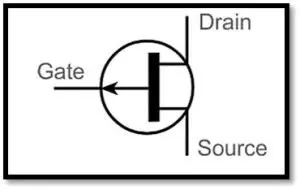
Junction Field Effect Transistor (JFET) Symbol:

Symbol of a JFET
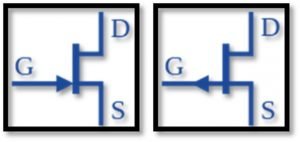
Symbol of a JFET

Picture2 Symbol
N- Channel and P- channel JFET

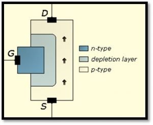
Picture3 Symbol
Typical layers of P-channel JFET

Junction Field Effect Transistor (JFET) Operation:

Picture4 Circuit

With VGS=0; applied voltage VDS causes a current to pass through from drain to source terminals.

If a negative gate to source voltage is applied, the depletion layer of the gate channel junction widens and channel becomes narrow. Thus, channel resistance is increased and id decreases for a given value of VDS. Because of small value of VDS, the depletion layer is uniform and the device acts as a voltage variable resistance. As value of VGS is increased in negative direction, depletion layer gets widened until it occupies the whole channel. This value of VGS is called the Pinch off voltage (VP).

As VDS appears along the channel length, voltage rises along the channel from source to drain. As a result, depletion layer becomes non-uniform. Reverse bias varies along the channel length and is highest at drain end and the depletion layer is widest at drain end. Hence channel resistance varies along the channel and characteristic curve becomes non-linear.

JFET Parameters:

Transconductance (gm)

In the meantime the, Junction Field Effect Transistor is a voltage controlled current source, the gain is the change in drain current divided by the change in gate voltage. This is termed the transconductance gain (shortened as gm) of the JFET

Transconductance is the ratio of change in drain current (δID) to change in the gate to source voltage (δVGS) at a constant drain to source voltage (VDS = Constant). So gm is fundamentally the slope of change of ID and in respect of change in VGS with constant VDS. It is given by,

DG 6

This value is maximum at zero the gate to source voltage (VGS = 0). The maximum value (gmo) is specified in particular Junction Field Effect Transistor (JFET) data sheet. . It is usually present in the units of conductance in particularly by unit Siemens. For FET, the standard values of Transconductance (gm) are in range of one to thirty milli siemens.

AC Drain Resistance, ( r)

It is the resistance between drain and source terminals, when Junction Field Effect Transistor is operating in the Pinch Off region. It is explained as the ratio of (ΔVDS), the variation in drain-source voltage to the variation in drain current (ΔID) at constant VGS – the gate-source voltage. So can be written as

DG 7

Amplification Factor (µ)

Amplification factor of a Junction Field Effect Transistor specifies just how much more control the gate voltage (VGS) has over the drain voltage (VDS). For example, if µ of a JFET is 30, it signify that VGS is 30 times as effective.

DG 8
µ=rd x gm

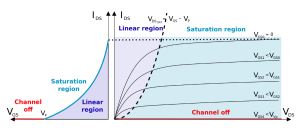
I–V characteristics and output plot of an n-channel JFET

The four different regions of operation for a Junction Field Effect Transistor are explained as follows:

Ohmic Region

If the Gate voltage is zero (VGS = 0) then the depletion layer is very minimal and the Junction Field Effect Transistor perform as a voltage controlled resistor.

Cut-off Region

During the Cut-off region, VGS – the Gate voltage, is sufficient to cause the Junction Field Effect Transistor to act as an open circuit as the channel resistance is at maximum. The Cut-off region is sometimes termed as pinch-off region also.

Saturation or Active Region 

During the Saturation region, the Junction Field Effect Transistor acts as a good conductor and is controlled by VGS– the Gate-Source voltage. Whereas during that period the drain to source voltage, (VDS) has little or negligible influence.

Breakdown Region 

In the Breakdown Region, The VDS – the voltage between the Drain and the Source, must be sufficiently high to causes the Junction Field Effect Transistors acts as a resistive passage to break down and to permit uncontrolled current.

Advantages of JFET:

  • High input impedance
  • Low noise
  • Small size
  • High frequency response

Disadvantages of JFET:

  • Junction Field Effect Transistor (JFET) has small gain bandwidth product
  • It has more vulnerability to damage during handling and maintenance.

Applications of JFET:

  • JFET is used as a switch
  • Junction Field Effect Transistor is used as an amplifier.
  • It can be used as buffer
  • Junction Field Effect Transistor (JFET) is used in digital electronics circuitry because of its size and applicability.
Encapsulado JFET
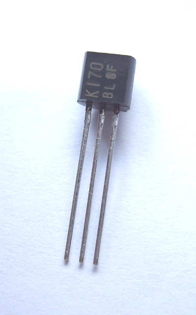
Toshiba K170
Image Credit:Euler666Encapsulado JFETCC BY-SA 3.0

BJT vs FET:

 BJTFET
PolarityBipolar deviceUnipolar device
Types of CarrierElectrons and Holes are two types of carrierEither electrons or holes are required here.
Process of Movement Movement of carrier is made by diffusion process.Movement of carriers are done by drift.
Switching SpeedSwitching speed of BJT is comparatively faster.Switching speed is comparatively slower.
Temperature DependencyLess temperature stableMore temperature stable
NoiseNoise level higherNoise level less
SizeComparatively biggerComparatively smaller, used in IC.
PriceComparatively cheaperComparatively expensive
Control ParameterCurrent control deviceVoltage Control device.
Input ImpedanceLow input impedanceHigh input impedance (in order of 1010 ohms)
GainCharacterized by Voltage gainCharacterized Transconductance

To know more about electronics click here
9 Facts On PNP Transistor:Diagram,Working,Applications,Cons

Circuit PNP 300x240 1

There are two types of standard bipolar transistors, namely PNP & NPN transistors. In this article, one of them, namely PNP, will be discussed in detail.

  • Definition of PNP Transistor
  • PNP Transistor Symbol
  • Diagram
  • Configuration
  • Working Principle
  • Applications
  • Advantages-Disadvantages
  • PNP Transistor as a Switch
  • PNP vs NPN Transistor

PNP Transistor Definition

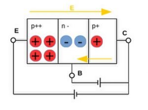
“A P-N-P Transistor is a BJT type built by merging an N-type semiconductor between two P-type semiconductors.”

PNP Transistor Diagram:

The transistor consists of three section-

  • E-Emitter
  • B-Base
  • C-Collector

On the subject of the working of three terminals of the PNP transistor,

  • The emitter is used to provide charge carriers into the collector through the Base area.
  • The Collector region gathers most of the charge carriers emitted in the emitter.
  • The base used to controls the quantity of current pass through the Emitter to Collector.

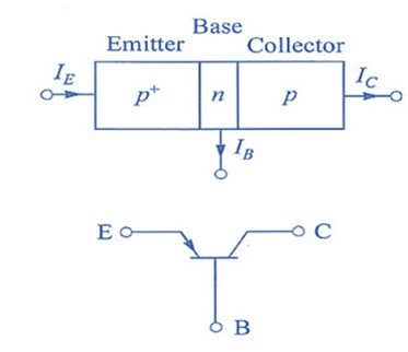
PNP Transistor Symbol

PNP Transistor Symbol
PNP symbol
Where, E=Emitter, B=Base, C=Collector

The mid-layer (N-type) is termed as the B- Base terminal. The left-sided P-type layer works as an E- Emitter terminal and the right-sided P-type layer known as a C-Collector terminal.

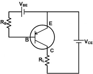
PNP circuit
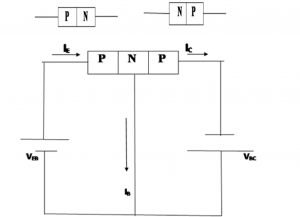
PNP Transistor

In an N-P-N transistor formation, One P-type semiconductor material is fit in between two N-type semiconductors, as explained in the article (Link NPN transistor). Whereas in a P-N-P transistor, one N-type semiconductor is fit in between two P-type semiconductors material.

In a PNP transistor, two types of diodes are used. They are respectively P-N and N-P diode. These P-N junction diodes are called the collector-base or C-B junction and base-emitter or B-E junction.

In the P-type semiconductor material, the charge carriers are holes primarily. So, in this transistor, the current formation is due to the movement of holes only.

The (P-type) Emitter and Collector regions are comparatively doped more than the N-type Base. The regions of the Emitter and Collector regions are wider in comparison to the base.

An adequately more number of free electrons are available in an N-type semiconductor, usually. But, the width of the mid-layer is narrower and lightly doped in this case.

PNP Transistor
Transistor Connection, Image Credit – S. BlankPNP TransistorCC BY-SA 4.0

PNP Transistor Working Principle

The Emitter-Base intersection is linked to forwarding bias. Along with also the +ve terminal of a voltage supply (VCB) is connected with all the Base terminal (N-type), and the -ve terminal is linked with all the Collector terminal (P-type). Consequently, the Collector-Base intersection is associated with reverse biasing.

As a result of this biasing, the depletion area at the E-B junction is less since it’s linked to forwarding bias. Even though the C-B junction is in reverse bias, the depletion area at the Collector-Base junction is wide enough. The E-B junction is forward biased. Therefore, more hole moves from emitters across the depletion area and acts as an input to the base. Simultaneously, not many electrons carried in an emitter in the base and recombined with the holes.

But the amount of electrons at the base is minimal since it’s a reasonably less doped and narrow area. Therefore, almost all Emitter regions’ holes will pass the depletion region and carried into the Base regions.

The current will pass through the E-B junction. This is Emitter current (IE). So IC, the Collector current will pass through the Collector-Base layers because of holes.

Circuit PNP
PNP Transistor Circuit

PNP Transistor Circuit

When a PNP transistor is linked with voltage resources, the base current will be carried in the transistor. Even the little quantity of base present controls the circulation of a massive number of current through the emitter to collector supplied the Base voltage is more -ve compared to Emitter voltage.

When VB the base voltage isn’t -ve in comparison to the VE the emitter voltage, the current can’t pass within the circuit. So, it’s necessary to provide a voltage supply in reverse bias > 0.72 Volt.

The resistors RL and RB are connected in the circuit. That to restricts the current to pass through the transistor’s maximum possible height.

The Emitter’s voltage is VEB as input side. Here the emitter current (IE) flows from the input side, and it flows in two directions; one is IB and other is IC.

IE= IB+ IC

But only 2 to 5 % of the total current flows in the IB, so IB is negligible.

Advantages of PNP Transistor

  • Small in size and could be utilized as a part of IC design.
  • Comparatively cheap, long-lasting and simpler circuit.
  • Spontaneous actions available
  • Low supply voltage requirement and less output impedance.
  • Produce less noise than NPN Transistors.

Disadvantages of PNP Transistor

  • Not suitable to operate on high-frequency application.
  • Perform slowly in comparison to NPN.
  • Temperature sensitivity and may get damaged during a thermal runaway.

PNP transistors Applications:

  • PNP transistors are applied as switches, i.e., analog switches, emergency push button etc. They have applications when emergency shutdown required.
  • These types of transistors are used in current sources circuitry, i.e., by exploiting the characteristics of current flows out of the collector.
  • It’s applied in the amplifying circuits.
  • They are used in Darlington pair circuits.
  • The P-N-P type transistors are used in heavy motors to control current flow and various robotic and microcontroller design applications.

PNP Transistor as a Switch

Once the switch is ON, the current will pass through the circuit and also behave as a close circuit. The transistor is an analogue power electronics-based circuitry with changeover characteristics which may function like ordinary switches.

As we have observed in the P-N-P transistor’s working, When the Base voltage isn’t more –ve than the VE, the current will not able to pass through the circuit. Thus, VB is at least 0.72 Volt in reverse bias connection to operate the transistor.

So, if the VB is 0 or > 0.72Volt, the current will not pass and operate as an open switch.

PNP vs NPN Transistor

comparison pnp npn
PNP TransistorNPN Transistor
PNP stands for Positive-Negative-Positive transistorsAn NPN Transistor stands for Negative-Positive-Negative transistor.
A PNP transistor needs negative current flow from the base to emitter.An NPN transistor needs positive current flow from the base to emitter.
A PNP transistor gets positive voltage at the emitter terminal. This +ve voltage permits the current emitter to collector.An NPN transistor gets +ve voltage in the collector terminal. This +ve allows the current to flow from collector to emitter.           

In the case of PNP transistor, the current directed from the emitter to base. Once the transistor is switched ON, current pass through the emitter to collector.  When current is supplied from the transistor base to emitter in an NPN transistor, the transistor base gets a positive voltage, and the emitter receives a negative voltage. Thus the current flows into the base. When there is enough current flowing from base into the emitter, the transistor is switched ON, and it directs the current flow from the collector to emitter instead of base to emitter.

To know more about electronics click here
11 Facts On Transistor :Characteristics, BandGap

Picture1 300x134 1

Contents

In this article we will discuss about the basic concepts related to transistor and its characteristics. 

Definition of a Transistor:

“Transistor is a semiconductor device with three connection parts. This device is mainly used for amplification to switching electronic signals application”.

Transistor Characteristics:

  • A transistor represents the relation between current and voltages.
    • It is a two-port network in general
    • Each of the transistor modes has different input characteristics, output characteristics, and current transfer characteristics.
    • A transistor has three poles, and each of the poles is made of N-type & P-type substrate mainly.

A transistor consists of three terminals

  • Emitter
  • Base
  • Collector

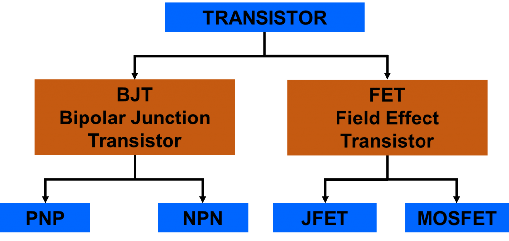
Transistor has divided into two key categories

  • Bipolar Junction Transistor (BJT)
  • Field Effect Transistor (FET)

There also exist three modes in a Transistor

  • Common Emitter or C-E Mode
  • Common Base or C-B Mode
  • Common Collector or C-C Mode

Diagram of PNP and NPN transistor

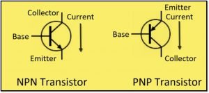
Picture1
PNP and NPN transistor

To know more about PNP and NPN transistors, first, we have to know about P-type and N-type semiconductors.

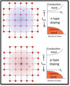
What is a P-type Semiconductor?

A P-type semiconductor (link) is a type of semiconductor when some impurity (mainly trivalent) is added to the intrinsic or pure semiconductor. In these types, the holes are majority and electronics are minority carriers. The trivalent impurities can be Boron (B), Gallium (Ga), etc.

What is N-type Semiconductor?

An N-type semiconductor is a type of semiconductor when some impurities (mainly pentavalent) are doped to an extrinsic semiconductor. In this, electrons are majority or primary carriers, and holes are minority or secondary carriers.

Some of the examples are Phosphorus (P), Arsenic (As) etc.

In N-type and P-type semiconductors, we observe different types of ‘energy bands’ which plays an important role in the function of a transistor; they are:-

Picture3

Image Credit: Tem5psuN and p dopingCC BY-SA 4.0

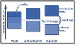
Band Gap

“The Band Gap refers to the energy difference between the top of the valance band and the bottom of the conduction band in an insulator and semiconductor.”

This is an energy range for solid basically where no electron states can be existent.

Picture4
Band Gap Diagram

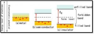
Forbidden Gap

In a solid, the range of energies than an electron within solid may have an energy band, and a range of energy that it may not have is called the forbidden gap.

Picture5
Forbidden Gap Diagram
Image Credit: S-keiBandGap-Comparison-withfermi-ECC BY-SA 2.5

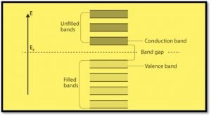
Valance Band and Conduction Band

In solid states, valance band and conduction bands are the bands closest to the Fermi level (a thermodynamic quantity denoted by µ) and determine the solids’ electrical conductivity.

Picture6
Valance and conduction Band

To build up a transistor, we need two types of semiconductors, which are:

1. Intrinsic semiconductor

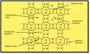
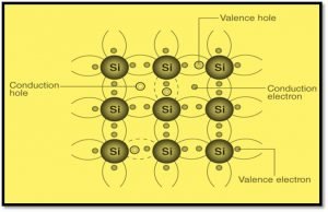
Picture7
Intrinsic semiconductor
  • – Materials are in pure form
  • – Low electrical conductivity
  • – No. of free electrons in conduction band = No. of the holes in the valance band
  • – Electrical conductivity be influenced by on the temperature.

2. Extrinsic semiconductor

Picture8
Extrinsic semiconductor

Extrinsic semiconductors are divided into further two types

  • n-type
  • p-type
  • – Impure material doped with p-type and n-type dopants
  • – Numbers of holes and electrons are not equal
  • – High electrical conductivity
  • – Impurities like Sb, P, ln, Bi are doped with Silicon and Germanium atoms.

Direct and indirect bandgap

In semiconductor electronics, a semiconductor’s bandgap can be classified in basic forms as follow:

  • Direct bandgap
  • Indirect bandgap.
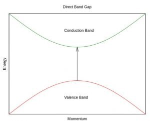
Picture9
Direct Bandgap

Picture10
Indirect bandgap

Dependent on the band structures, substances have a direct bandgap or indirect bandgap.

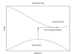
  • The direct band-gap occurs when the momentum of the low-energy level from conductive region and high-energy level from valence region are similar.
  • The in-direct band-gap occurs when the momentum of the low-energy level from conductive region and high-energy level from valence region are not similar.
  • When an electron has sufficient energy, they can reach to the conductive band. In this process, photons are being emitted.  
  • For an indirect bandgap material, both photon and phonon has be included in a transition from upper valence band top to the lower conduction band.

The max-energy state in the valence band and the min-energy state in the conduction band are distinguished by the Brillouin zones k-vector or a particular crystal momentum. In the event the k-vectors are distinct, the substance has an “indirect gap”. The bandgap is known as direct if the crystal movement of holes and electrons is the equal in the conduction and valence bands; an e could emit a photon. A photon can’t be emitted within an “indirect” gap since the electron has to pass through an intermediate one and transfer momentum into the crystal lattice.

What is semimetal material?

In certain substances with a direct gap, the value of the difference is negative. Such substances are called semimetals.

Moss–Burstein Effect

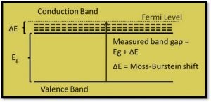
The Moss-Burstein effect or Burstein-Moss shift is the prodigy where the bandgap of a semiconductor may increase.

  • This is witnessed for a degenerate electron distribution or in some variant of semiconductors.  
  • As per Moss-Burstein shift the Band Gap is
Picture11
Moss–Burstein Effect

Apparent Band Gap = Actual Band Gap + Moss-Burstein shift

In ostensibly doped semiconductor, the Fermi level is to be found between the valence and conduction bands.

For example, in an n-type semiconductor, as the doping concentration increases, electrons populate in the conduction regions that compels the Fermi level to higher energy label.

The Fermi level is located in the conduction band for degenerate amount of doping. Pauli’s exclusion principle prohibits excitation for these pre occupied states. Thus an increase s observed apparently in the bandgap.

To know more about electronics click here

Facts On Transistor Amplifier :7 Classification & 4 Types

Picture No of Stage 300x190 1

In this article, different transistor types will be discussed, primarily related to bipolar junction transistor (BJT) and field-effect transistor (FET) and their characteristics. However, transistors have been used as an amplifier in different circuits and various stages, mode, configurations, etc. That will also be discussed.

Although there are diverse classification of the amplifier as per different parameters are as follows:

Transistor Amplifier Classification

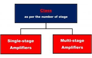
Transistor Amplifier Class: as per the number of stages

As per the number of stage of amplification, there are two class is available in transistor amplifiers, are

Picture No of Stage

Single-stage Amplifier

− The circuit comprising one transistor circuitry for only step of amplification.

Multi-stage Amplifier

– This circuitry has multiple transistor circuits that be responsible for multi-stage amplification in the course of operation.

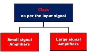
Transistor Amplifier Class: as per the input signal

As per the input signal’s level the categorization are as follows:

Picture As Input Signal
transistor amplifier
Image credit :Filip Dominec, Transistor amplifier designCC BY-SA 3.0

Small signal Amplifier

− If the input signal is very weak to generate minor or insignificant fluctuations in the collector current than quiescent value, then it’s termed as a small-signal amplifier circuit.

Large signal amplifier

− If the fluctuations existing in collector current are to be high enough, then it’s is termed as a large-signal amplifier circuit.

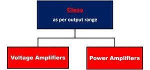
Class as per its output

If the output is considered as parameters, then the amplifier can be of two types. They are – Voltage Amplifiers and Power Amplifiers.

Picture Output Range

Voltage Amplifier

− It is the amplifier circuit that increases the input signal’s voltage level (V0) is called a Voltage amplifier.

Power Amplifier

− It is the amplifier circuit that increases the input signal’s power level (P0) is called a Power amplifier.

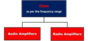
Transistor Amplifier Class: as per the frequency range

As per the signals freq. range, there are two types of an audio amplifier and radio amplifier.

Picture Frequency

Audio-Amplifier

− The audio amplifier circuit capable of amplifying the input signal in the range marked for audio signals, i.e., Frequency Range: from 20Hz to 20 kHz range.

Radio-Amplifier

−The radio amplifier capable of amplifying the input signal in the radio frequency range or lie in a very high-freq. range.

Transistor Amplifier Class: as per Biasing and mode

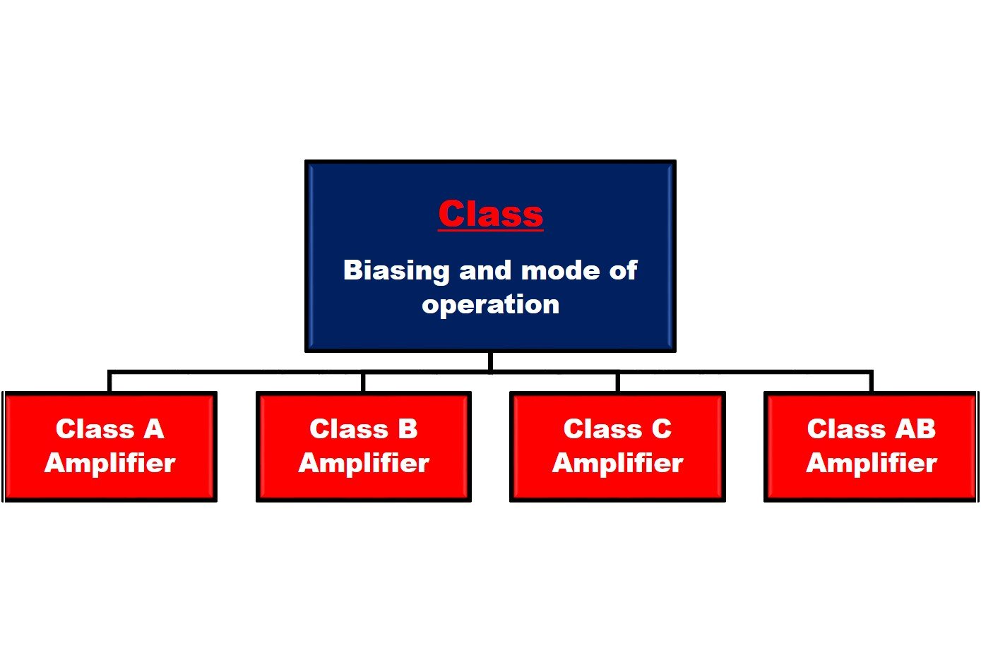
As per the biasing and mode of operation, classifications are class A, class B, class C, and Class AB type transistor amplifiers. The condition is as follows:

Picture Biasing

Class-A Amplifier

− The collector current carried through for the entire cycle (One Cycle) of applied alternative current signal.

Class-B Amplifier

− The collector current pass through for half-cycle (equal to 0.5 Cycle)  of applied input alternative current signal.

Class-C Amplifier

− The collector current carried for the less than half the cycle (< 0.5 Cycle) of applied input alternative current signal.

Class AB amplifiers

− Class AB amplifiers: Class AB amplifiers are formed by combining A and B classes. It helps to achieve all the gains as well as it eliminates the negatives.

Transistor Amplifier Class: Based on Configuration

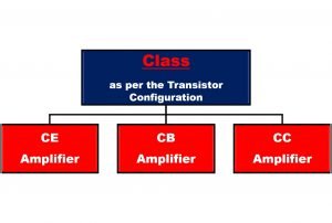
Transistor Amplifier Classes: There are three types on the basis of configurations. They are – Common Emitter, Common Collector and Common Base types. 

Picture Transistor Configuration

C E or Common Emitter Amplifier Configuration

− The amplifier circuit formed using a Common Emitter configured transistor combination is called a CE amplifier.

C B or Common Base Amplifier Configuration

− The amplifier circuit formed using a Common Base configured transistor combination is called a CB amplifier.

CC or Common Collector Amplifier Configuration

− The amplifier circuit formed using a Common Collector configured transistor combination is called a CC amplifier.

Transistor Amplifier Class: Based on Coupling method

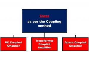
There are three types on the basis of Method of coupling. They are – Resistor-Capacitor Coupled, Transformer Coupled, and the last one is the Direct Coupled.

Picture Coupling Method

Direct-Coupled Amplifier

− If a multi-stage amplifier is coupled directly to the subsequent stage.

RC-Coupled Amplifier

− A Multi-stage amplifier coupled to the subsequent stage using a resistive and capacitive (RC) element via a combination circuit then it is termed as an RC coupled amplifier.

Transformer-coupled Amplifier

− A Multi-stage amplifier coupled to the subsequent stage by means of a transformer based circuit, then it is a transformer coupled amplifier.

The Types of Transistors:

There are several transistors available in the market as per different applications. The important types are as follows.

This image has an empty alt attribute; its file name is 1-1024x486.png
Transistor Type

Bipolar Junction Transistor (BJT)

A BJT is a type of transistor, has both electrons and holes. Electrons, as well as the holes, act here as charge carriers.”

  • Bipolar junction transistor is a current controlled device.
  • A Bipolar junction transistor (BJT) has two PN junctions for its functioning.
  • There are two types of standard transistors, which are bipolar; PNP & NPN.
  • There are three leads in a transistor, labeled as Base (B), Collector(C), and Emitter (E).

PNP Transistor

In P-N-P transistors, two types of diodes are assembled here. They are P-N and N-P.

The transistor consists of three section-

  • − Base
  • − Collector
  • − Emitter

In the PNP configuration, the transistor P junction has many holes, and the intermediate junction called N has efficiency and electrons. Now, the EB junction becomes the reverse biased and the CB junction becomes revere bias.

Due to the connection the bias formed and the holes started flowing from P junction. After that, the flow continues towards the N region. Here recombination takes place. The rest of the holes again flow towards the N. Now, the current through the emitter is known as Emitter Current which goes into two side. One is the Base Current another is the Collector current.

IE=IB+IC

But 2% of the total current flows in the IB, so IB is negligible.

Hence, IE=IC

NPN Transistor

In the NPN configuration of a transistor, two types of diodes are used: N-P & P-N.

As mentioned earlier, a transistor has three Terminals. They are – Collector, Emitter and Base.

Due to the connection the bias formed and the holes started flowing from N junction. After that, the flow continues towards the P region. Here recombination takes place. The rest of the holes again flow towards the P. Now, the current through the emitter is known as Emitter Current which goes into two side. One is the Base Current another is the Collector current.

IE=IB+IC

Field Effect Transistor (FET):

In a field-effect transistor, only an electrical field is used to control the flow of current. They have three terminals, which are Source, Drain, and Gate. FETs are unipolar transistors.

Read more about Differential Amplifier.

To know more about electronics click here
11 Types of Transformers(Beginner’s Guide !)

power transformer

Content: Types of Transformer

  1. Types of transformer
  2. Classification parameters
  3. Ideal transformer
  4. Real transformer
  5. Step-up transformer
  6. Step-down transformer
  7. Power transformer
  8. Single phase transformer
  9. Three- phase transformer
  10. Instrument transformer
  11. Pulse transformer
  12. RF transformer
  13. Audio transformer
  14. Transactor
  15. Difference between Step up and step down transformer
  16. Difference between single phase and three phase transformer

Types of Transformers

There are many types of transformers based on classification parameters described below. We will discuss some of the transformer types and their workings. List of transformers we will discuss are the followings –

  • A. Ideal transformer
  • B. Real transformer
  • C. Step-up transformer
  • D. Step down transformer
  • E. Power transformer
  • F. Single – phase transformer
  • G. Three- phase transformer
  • H. Centre tapped transformer
  • I. Instrument transformer
  • J. Pulse transformer
  • K. RF transformer
  • L. Audio transformer

Know about Transformer Definition, Construction & Applications. Click Here!

Classification Parameters

There are different types of transformer classification parameters based on which we can classify the transformer. Some of them are –

  • Voltage Class: Transformer can be classified based on the voltage used by them. From a few volts to megavolt amount of voltage can be used by transformers.
  • Power Rating: Transformers have ratings range from few Volt-Amperes to mega Volt-Amperes.
  • The number of turns in primary and secondary windings: Step down transformer, step-up transformer.
  • Construction of core: Depending on the transformer’s core construction, they can be classified into two types. They are shell types and core types.
  • Cooling Type: Transformers can be classified upon the cooling types. There are several types of transformer – self-cooled, oil-cooled, forced cooled, etc.
  • Application type: Based on transformer’s various applications like – energy transfer, power distribution, voltage-current stabilizer, isolation, etc., they can be classified into enormous kinds.

Ideal Transformer

Ideal transformers are theoretical transformer that suffer no losses and provides 100% efficiency. An ideal transformer can not be made in reality and present only in imagination.

Real Transformers

Every transformer which we can use in the real world is real transformer.

A real transformer can not achieve 100% efficiency as it will suffer some loss of power. There are many types of transformer power-loss can be found. Some of them are – Eddy current loss, Hysteresis loss, dielectric loss, etc.

Step-up transformers

This types of transformer increases voltage, which is applied to primary windings. The secondary windings supply the higher voltage.

The number of turns of the secondary transformer is higher than the number of turns in the primary windings.

Step-up transformers found its application in transmission line carrying high voltage.

Step-down transformers

This types of transformers does the opposite of a step-up transformer.

Step-down transformers reduce the voltage that is applied to its primary windings. The secondary windings supply the lower voltage. Many home appliances, power distribution systems, and many other electrical fields use this type of transformer.

Power transformers

Power transformer is the one particularised for the distribution of power. They are very high rated transformers and are designed for 100% efficiency. They are extensive and useful for delivering needed and limited power for consumers.

power transformer
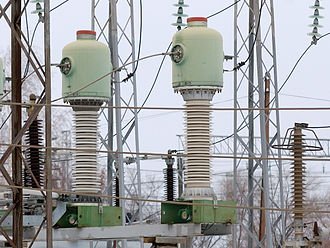
Power Transformer at substation, Image Credit – Ptrump16Substation transfomerCC BY-SA 4.0

Single-phase transformers

Transformer working on faraday’s law and having two windings are single-phase transformers. The windings are known as primary and secondary windings. Without varying the frequency and power, this transformer transfers AC energy.

sp transformer
Single phase transformer, Image by – Hannes GrobeTransformer-1 hgCC BY-SA 4.0

Three-phase transformers

Three single-phase transformers are connected to form a three-phase transformer. All three primary windings are combined to form a single primary winding, and also all three secondary windings are combined to form a single secondary winding. Star and delta are the types for primary and secondary connections. The combination of primary and secondary windings are all possible combination of star and delta type.

This types of transformer is generally used for industrial purposes.

Assembling of three single-phase transformer is less costly than buying a three-phase transformer.

3p transformer
Types of Transformer :Three Phase Transformer, Image Source – High ContrastPylon transformer in SyriaCC BY 3.0 DE

Centre tapped transformers

A centre tapped transformer works almost in the same way a normal transformer works. The only difference is that its secondary windings has two parts and from that individual voltages can be acquired. The tapping point lies in the centre of the secondary windings and that divides the secondary windings. The tapping point provides a common connection for opposite and equal secondary voltages.

ct transformer
Diagrammatic Representation of a Centre Tapped Transformer

Instrument transformers

Instrument transformer is a special type of transformer used for transforming or isolation of current and voltage. It is a high accuracy device. An instrument transformer’s main use is to isolate high voltage connected primary windings from the meter connected with the secondary windings.

It has two types. The series-connected type is known as the current transformer, while the parallel-connected transformer is known as potential or voltage transformer. Current transformer steps down the current while the voltage transformers do the same for voltage of a supplied power.

Some advantages of using Instrument transformer are that –  large current and voltage of Alternating Current power can be measured by using a low power rated instrument transformer, many measuring instruments can be connected using a single instrument transformer to power system, measuring instruments can also be standardized.

in transformer
Types of Transformer : Instrument Transformer, Image Source – Vivan755SF6 current transformer TGFM-110 RussiaCC BY-SA 3.0

Pulse transformers

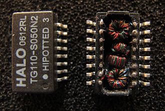
Another special type of transformer is the pulse transformer. It is used for transmitting rectangular electrical pulses. It transmits pulse of voltages between load and the windings. It has high open-circuit inductance, distributed capacitance, and low leakage induction. Depending on the types, it has several applications. Small versions are used in digital logic circuits. Medium versions are used in power-controlling systems. In contrast, larger versions are used in the power distribution system. Various pulse transformers have a wide range of applications like radar, power semiconductors, and high energy power applications.

There are some parameters which measures the performance of a pulse transformer. Some of them are – repetition rate, pulse width, duty cycle, current, frequency, input – output voltages, etc.

The main advantages of a pulse transformers includes that they are small in size, less costly, provides a high isolation voltage and operates at high frequency. The disadvantage includes – saturation current of the core can get reduced because of the direct current through the primary windings.

pulse transformer
Types of Transformer :Pulse Transformer. Image Source – wdwd, Impulstransformatoren TG110 TopBottom CCC BY-SA 3.0

RF transformers

The transformers used in the radio frequency domain is known as RF transformer. This devices transfers energy in circuits with the help of electromagnetic induction. Steel as a core structure is prohibited in this type of transformer. It has several types too. Air core(low inductance, PCB use), Ferrite core(baluns for TV and radios), and transmission line transformers are some types. Low power circuit is ideal for the use of this transformers. Some important specifications of a RF transformers are – range of operating frequency, bandwidth, unbalance amplitude and phase, operating temperatures etc.

Audio Transformers

The transformers used in audio circuits are known as audio transformer.  Audio transformer has various applications.

Previously audio transformers were made to isolate different telephone systems while keeping their power supplies isolated. Carrying an audio signal is its main objective. It can be used to match impedance like low impedance loudspeaker can be matched with high impedance amplifiers.

Audio transformers also do interconnection of professional audio system components, elimination of buzz and hum. Loudspeaker transformer, inter-stage and coupling transformers, small-signal transformers are some of its types.

audio transofrmer Updated
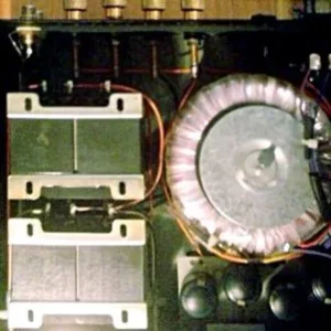
Types of Transformer :Audio Transformer, Image Source – Adamantios, Audion-sterling-transformersCC BY-SA 3.0

Transactor

A transactor is a combined device of the reactor (inductor or choke coil) and a transformer. Air – core present in the device used to limit the coupling between windings.

Difference between Step up and Step down transformer

Subject of ComparisonStep down transformerStep up transformer
Number of turns in windingsHigher no. of turns in primary windings, lower no. of turns in secondary windings.Lower no. of turns in primary windings, higher no. of turns in secondary windings.
WorkingReduce the input voltage applied in the primary windings.Increases the input voltage applied in the primary windings.
Voltage -CurrentHigh input voltage, Low output voltage and high current in the secondary side.Low input voltage,  high output voltage and low current in the secondary side.
Size of conductorSecondary windings are made up of thick insulated copper wire.Primary windings are made up of thick insulated copper wire.
Power RatingComparatively lower than Step-up transformer. The range lies under 110 volts.Comparatively higher than step down transformers. Rated above 11,000 volts.
UsesMany home appliances, voltage converters.Power distribution system, X-Ray machines etc.
Types of Transformer, Table – 1

Difference between Single phase and three phase transformer

Subject of ComparisonSingle phase transformerThree phase transformer
Working principleOne conductor supplies power.Three conductor supplies power.
Voltage carried230 volts415 volts
Phase Split phaseNo special name
Required no. of wireRequire two wires for making the circuit.Requires four wires for making the circuit.
CircuitrySimple networkComplex network
Power failureMay occursDo not occur
Power LossMaximum power loss occurs hereMinimum amount of power loss occurs here.
EfficiencyLower than three-phase transformer.Higher than single phase transformers.
EconomicalLess economicalMore economical
ApplicationsSpecially for home appliances.Industrial purposes.
Types of Transformer, Table – 2

Find out Frequently Asked Questions on Transformer & Numerical Problems. Click to proceed!

7 Facts On Transformer:Losses,Efficiency,Working

640px Current transformer 27 hg

Content

Working Principle of a Transformer

The transformer works on Faraday’s Law. Faraday’s law states that –

““Any changes in the coil of wires’ magnetic-fields, will cause an induction of emf. The magnitude of the induced potential is identical to the flux’s changing rate.

It can be written as –

E = – N * dϕ/dt

E is the induced emf, & N, ϕ is the number of turns and the magnetic flux produced, respectively.

The negative sign represents that the change in the magnetic field’s direction is opposite to induced emf. It is also known as Lenz’s law.

Now, we know that transformers have two windings. The alternating power is applied to the primary windings. The flow of current causes generation of a magnetic field around it. This property is known as mutual inductance. Now the current flows according to Faraday’s Law. The maximum strength of the magnetic field will be equal to d ‘phi’/dt. Magnetic lines of force now expand outside from the coil. The soft iron core concentrates the field lines and forms a path. The magnetic fluxes connect the primary windings as well as the secondary windings.

640px Current transformer 27 hg
Current transformer, Image Credit – Hannes GrobeCurrent-transformer-27 hgCC BY-SA 4.0
transformers
Working of a transformers, Image Source –  Fred the OysterTransformer FluxCC BY-SA 4.0

Now, as the flux also passes through the secondary windings, a voltage generates there. The induced emf’s magnitude will be given according to Faraday’s law. It will be = N * dϕ /dt.

The frequency and power of the supplied voltage never change in the whole process.

The induced voltage depends on the turn’s ratio.

Know more about structure and construction of Click Here!

Transformer EMF Equation

Let us assume magnitude flux as phi.

We know that magnetic flux varies sinusoidally.

So, ϕ = ϕm * sin (2 * π * f * t)

f is the frequency of the flux and N is the number of turns

Now, E = N * dϕ/dt

or, E = N * d (ϕm sin (2 * π * f * t)) /dt

or, E = N * 2 * π * f * ϕm * cos (2 * π * f * t)

For E =Emax, cos (2 * π * f * t) = 1

Emax = N * 2 * π * f * ϕ m

Now, Erms = Emax / 2

Erms = N * 2 * π * f * ϕm / 2

Erms = 4.44 f * N * ϕm

This is known as Transformer EMF Equation.

Losses of a Transformer

Loss in an electrical device or circuit means loss of power. A real transformer has different types of losses, but an ideal transformers never suffers a loss. There are several types of loss inside a transformer. Some of them are –

  • A. Core Loss / Iron Loss
  • B. Copper loss or Ohmic Loss
  • C. Stray Loss
  • D. Dielectric Loss

A. Core loss / Iron Losses:

  • The loss occurs due to alternating flux, inside the iron core is known as Core Loss or Iron loss. This type of losses are known as No Load Losses.

There are two categories of core loss. They are –

  • i) Hysteresis Loss
  • ii) Eddy Current Loss

i) Hysteresis Loss –

An alternative magnetic force generates in the core of the transformer. That magnetizing force causes a hysteresis loop and that causes hysteresis loss.

Ph = η * Bmax * n * f * V

Ph = Hysteresis Loss

η = Steinmetz hysteresis coefficient

Bmax = Maximum flux density

n = Steinmetz exponenet

f represents the magnetic reversal per second

V = volume of magnetic material

Hysteresis loss contributes 50% of no load loss.

ii) Eddy Current Loss

Faraday’s Laws are behind the cause of Eddy Current Loss. The magnetic-fluxes cause a potential in the core. Now, due to this emf, current flows. This current is termed as Eddy Current and it is an undesired current. Loss due to this current is Eddy Current Loss.

The eddy current loss is expressed as –

Pe = Ke * Bmax2 * f * V * t2

Pe = Eddy Current loss

Ke = Eddy current constant

Bmax refers to the maximum flux density and f is the frequency of the magnetic reversal per second.

V = volume of magnetic material

t = magnetic thickness

B. Copper loss or Ohomic Loss:

  • This type of loss occurs due to the windings’ wire resistance. If Ip, Rp is current and resistance of primary winding and Is, Rs is current and resistance of secondary windings, then the loss will be given by the equation –

Po = Ip2Rp + Is2Rs

As the wires are of coppers’, the loss is termed as Copper loss. This type of loss is also known as Load Losses because this loss occurs only when load is connected with the secondary windings.

C. Stray Loss:

  • The reason behind such losses is the leakage field. It is a negligible loss.

D. Dielectric Loss:

  • The transformer’s insulator causes this type of loss.

There are also losses due to distorted voltage and currents.

640px Electric insulators on top of a transformer 2
Insulators on the top of a transformer, Image Credit – High ContrastElectric insulators on top of a transformer (2)CC BY 3.0 DE

The efficiency of a Transformer

The efficiency is the ratio of the produced power in the input to the supplied power of the output. It is represented as – η.

η = Output power /Input Power * 100%

In an ideal transformer, η comes as 1, which means Output power is equal to the input power. But in reality, a transformer suffers losses.

Loss = Input Power – Output Power

Or, Output Power = Input Power – Loss

So, Efficiency –

η = (Input Power – Loss) / Input Power * 100%

η = 1 – loss/ Input Power * 100%

Frequently Asked Questions

1. How is a transformer rated?

Transformers are rated in volt-amperes or kilo-volt-amperes (kVA). This rating indicates that the primary windings and the secondary windings are designed to tolerate the rated power.

2. How many types of Transformers are there?

There are many types of transformers based on different parameters. Some of them are –

  • Ideal Transformers
  • Real Transformers
  • Step-up types
  • Step down type
  • Power transformer
  • Single – phase types
  • Three- phase types
  • Centre tapped types
  • Instrument types
  • Pulse types
  • RF types
  • Audio types

3.  A transformer has a turn’s ratio of 16 to 4 or 4. If the transformer secondary voltage is 220 V, determine the primary voltage.

We know that

Turns ratio =NpNs =VpVs

Here, Np = 16

Ns =4

Vs = 220 v

we have to find Vp

so Vp = Np*Vs/Ns = 16 * 220 / 4

Vp = 480 volt.

So the primary voltage was 480 volt.

4. What is the Reversibility of Transformer Operation?

Reversibility of Transformer Operation means using the transformer from backward. That is, giving the secondary windings an input voltage and connecting load at the primary windings.

5. Do the transformers perform in DC voltage?

No, a transformer does not perform in DC voltage. Applying Dc voltage will cause over hitting of the primary windings as the signal finds it a short-circuit.

6. What is Impedance matching?

The concept of impedance matching is that when a source voltage is connected to load, the load get the maximum power if the impedance of load is equal to the impedance of the impedance of the fixed internal source .It is one of the application of transformers.

7. A single phase transformer is with a rating of 2 kilo volt ampere has a 400v at primary windings and a 150v at secondary windings. Find out the primary and secondary full load current of the transformer.

Primary full-load current = 2kVA x 1000 / 400 V = 5 A

Secondary full-load current = 2kVA x 1000 / 150 V = 13.33 A

8. A transformer has 500 turns in the primary windings and 20 turns in the secondary windings. Find out –

a) The secondary voltage if the secondary circuit is open and the primary voltage is 100 v

b) Find out the current in primary and secondary windings when the secondary winding is connected to a resistance load of 16 ohms.

We know that turns ratio is given by

Turns ratio  = Np/Ns = Vp/Vs

Np is the number of turns in primary windings.

Ns is the number of turns in secondary windings.

Vp is the voltage at primary side.

Vs is the voltage at secondary side.

Now we can write

Vs = (Ns * Vp) / Np

Or, Vs = (20*100)/500 V

Or, Vs = 4 V

Now for the second case, we know that power remains unchanged while transferring energy through a transformer.

We can write,

Pp = Ps

Where Pp is the power in primary side and Ps is the power from secondary side.

Pp = Vp * Ip

Ps = Vs * Is

Ip is the current in primary side and Is is the current in secondary side.

So, Vp *Ip  = Vs * Is

Or, Ip = (Vs * Is) / Vp

Or, Ip = ((Vs*(Vs/Rs) / VpFrom ohm’s law V= IR, thus I = V/R, Here Rs is the resistance of the secondary coil.

Or, Ip = (Vs * Vs )/ (Vs * Rs)

Or, Ip = 4*4 / 100*16, Substituting the values and Rs = 16 ohm was given in the question.

So, Ip = 10 mili – ampere.

And, Is = Vs/ Rs

Is = 4/16 A = 0.25 A

To know more about transformers and electronics click here
Electrical Transformers:Structure,Construction,Applications

660px Transformer Flux.svg 1

Content

What is Electrical Transformer?

As the name suggests, an Electrical transformer transfers energy. A formal transformer definition will be –

“It is a device that transfers electrical energy between electrical circuits.”

It is a passive device. It uses Faraday’s law to transfer energy without any metallic contact. Electrical transformers are one of the useful and needed device for the power distribution.

History related to transformers

Miksa Deri, Otto Blathy and Karoly Zipernowsky are considered to be first designer of the first transformer. They also implemented transformer for commercial systems. Though the Law of induction was given by Faraday in 1830’s and Rev. The induction coil was invented by Nicholas Callan in the year 1836. In the meantime Thomas Alva Edison came up with the idea of Electric Bulb in the year 1882.

Basic Structure of Electrical transformers

A single phase electrical transformer consists of three main components. They are – Primary Windings, Secondary Windings & the Magnetic Core.

  • Primary Windings – It is the part that is connected with the source. It is made up of coils of wire. Magnetic flux initially produces here.
  • Secondary Windings – It is the part that is connected with the load. It is also made up of coils. There is a turn’s ratio that defines the number of turns of the wire to make both the windings’ coils. There is no metallic connection between primary windings and secondary windings, as mentioned before.
  • Magnetic Core – It is the iron structure that wraps up both the primary and secondary windings. It is a soft iron core, made up of small elements to reduce the core’s losses.

Construction of Electrical Transformers

The construction of Electrical transformers depends on how the primary and secondary windings are wrapped around the iron core structure.

There are two categories of transformers. One is Closed-core type and another is Shell-core type.

A. Closed Core Transformer –

  • Here, both the windings are wrapped from outside of the core. (Both windings means – Primary Windings and Secondary Windings). In this construction, windings wrap-up every legs of the core. Half of the primary windings and half of the secondary windings are kept on over other densely on each leg. Magnetic flux passes by this process and increases magnetic coupling. This type of transformer has a drawback, known as – ‘leakage flux.’
Transformer Core
Structures of of core type transformers

B. Shell Core Transformer –

  • In this type, both the primary and secondary windings are inside the iron core. Here, the iron core forms a shell-like Structure for the windings, that’s why it is known as Shell Core Transformer. The windings share the same center leg, which has a cross-sectional area twice as the outer legs. This type of transformers overcome the issue of ‘leakage flux.’
Ideal transformer.svg
Shell Type transformers , Image source – !Original:Constant314Vector: WikimpanIdeal transformerCC0 1.0
  • Windings: Windings are the current-carrying part of the transformer.  Mainly copper or aluminium wire is used to make the coil of the windings. Transformer coils and windings can be classified into two main categories. They are – Concentric Coils and Sandwich Coils. Sandwich Coils are generally used in Shell Type Transformer. Alternate discs are made to spiral form.
  • There are also Helical Windings, which are used in low voltage, high power applications. There are some insulators inside every type of windings. Insulators are one of the important elements for electrical transformers.
  • Cooling:  Cooling of a device helps the machine to operate more years flawlessly. Some electrical transformers need forced cooling, and some are self-cooling types. Forced cooling includes cooling by oil, water, or both. Large transformers with high power ratings are filled with transformer oils, which cool and insulate windings. Some transformers are filled with gases for cooling.
  • Insulation: Insulation is necessary between turns of windings, between two windings, between core and windings. Layers of papers and polymer films are used as insulators. Large insulators use transformer oil as insulation purposes.
  • Bushing: Bushing is a hollow electrical insulator that allows a conductor to pass through a barrier. Large, high rated transformers has bashings made up of porcelain or polymers.

The polarity check of Electrical Transformers

An Electrical transformer’s polarity is defined as the direction of induced emf in both the primary and secondary windings. It is of two types –

  • A. Additive Polarity
  • B. Subtractive Polarity

A. Additive Polarity

-In this type of polarity, the same polarity terminals are connected in both the windings.

B. Subtractive Polarity

– In this type of polarity, different polarity terminals are connected in both the windings.

What does the transformer do?

Electric transformers increases or decreases the supplied voltage and current. It does not change the frequency or the power of the supplied electrical signal. The need for using a transformer is that electrical appliances need a certain amount of voltage, which is lower or higher than the supplied power. For example, a LED which works on 1.5 volts – 2 volts will blow out if we connect it to a normal household rated power supply. So we need to use a step down transformer to use the LED.

640px Current transformer 17 hg
Current transformer, Image Credit – Hannes GrobeCurrent-transformer-17 hgCC BY-SA 4.0

Click here to know about Working Principles, Efficiency and Losses of a transformer.

Application of a Transformer

Transformers has a lot of applications in today’s world. Some of them are –

i) Power Distribution:

  • A large amount of voltage is produced in the power stations. But we cannot use that voltage directly for our household applications. In this time, a transformer comes into action. Transformers stepped down the voltage to our required voltage. This type of transformer is known as power transformers. There are also transformers which steps up the voltage. Because of this type of transformer it is possible to provide electricity to houses.
640px Pylon transformer in Syria 1
Transformers in power distribution , Image source – High ContrastPylon transformer in SyriaCC BY 3.0 DE

ii) Electronic Devices:

  • Many electronics devices and home appliances use transformer either for stepping up voltages or stepping down voltages as per requirements.
Electrical Transformer
Transformers for electronics uses, Image Source – Retired electricianSMPS transformers (Korea, around 2000) – bottom viewCC0 1.0

iii)Audio transformers:

  • This type of transformers allows telephonic circuits to allow a two-way conversation over a single pair of wire. They also interconnections between audio systems. It can be used to match impedance like low impedance loudspeaker can be matched with high impedance amplifiers.
  • Three phase transformers have wide use in industrial purposes where single phase transformers can not serve the purposes.
  • Instrument transformers can isolate two device or system using its properties.
  • Radio frequency transformers or RF transformers are used in Radar like devices and has application in radio frequency domain.
  • Pulse transformers are used for transferring electric pulses in electronic circuits, digital circuits and in power distribution and controlling system.

Advantages & disadvantages of using a Transformer

Advantages of Electrical transformers

Transformers are used for various purposes because of its advantages. Some of the advantages are –

  • Transmits Power: Transformers allow transmitting of electrical signal over long distance. The resistance of the transmission line get reduced after increasing the voltage and that is possible only by transformers. Thus, the power loss is less and electricity can be supplied to every household. Otherwise the resistance would be so high that it is quite impossible to supply.
  • Continuous workings: Transformers can work continuously over long times. It does not need to switch off in a day or give rest.
  • Low Maintenance: Transformers not only works continuously but also they need not high maintenance. Checking oil, cleaning the parts are the only maintenance a transformer needs. Also, the maintenance does not cost much and also not time consuming.
  • No delay: Transformers has no delay while starting. It starts operation immediately. Once a transformer is implemented, it starts immediately.
  • Efficient: Though transformers suffer losses but they are efficient enough for distribution economically. Almost 95% efficiency is achievable.

Disadvantages of using Electrical Transformers

Few disadvantages are –

  • Larger in size : Though there are transistors that are small in size but as the voltage rating increases the transformer size get increased too. Not only the basic structure increases, the cooling system size get increased too. So it takes a lot of space to accommodate.
  • Requires a cooling system: Transformers operates continuously and it produces a lot of heat. So to operate in a efficient way, a transformer need a cooling system attached with it.
  • AC working only: Transformer works only for alternating current or AC voltages as it need time varying current to produce magnetic flux. Connecting with a DC voltage will burn out the transformer.

To know more about electronics click here
23 Analog Filter Interview Questions (For Beginner’s !)

Analog Filter related selected MCQ Questions has been discussed in this article particularly for Core Technical Round Electronics domain interview. This is useful for different competitive and Semester Exam.

Q. The input-terminals of an op-amp are termed as

  1. High & low terminals
  2. Differential & non-differential terminals
  3. Inverting and non-inverting terminals
  4. Positive & negative terminals

Ans-(3)

Q. In a series resonance circuit, to obtain a LPF character, across which, output voltage should be measured?

  1. Inductive element
  2. Resistive element
  3. Capacitive element
  4. All of these

Ans-(3)

To learn about low pass filter and it’s characteristics click here
Q. In a series resonance circuit, to get a high-pass filter character, across which, output voltage should be measured?

  1. Resistive element
  2. Inductive element
  3. Capacitive element
  4. All of these

Ans-(2)

Q. A high pass filter is mainly

  1. A differentiator circuit with low time constant.
  2. A differentiator circuit with 0.75 time constant.
  3. An integrator circuit with small time constant.
  4. An integrator circuit with 0.50 time constant.

Ans-(1)

Q. The transfer function of an low-pass RC network is

  1. RCs/1+RCs
  2. 1/1+RCs
  3. RC/1+RCs
  4. s/1+RCs

Ans-(2)

Q. For a high-pass-RC circuit, when exposed to a unit step function, across capacitor voltage will be

  1. e-t/RC
  2. et/RC
  3. 1
  4. 1-e-t/RC

Ans-(4)

To learn about high pass filter and their advantages, disadvantage and characteristics click here
Q. In low-pass filter, at which frequency the highest point of the graph occurs?

  • At f resonant
  • Below f resonant
  • Above f resonant
  • At any frequency

Ans-(2)

Q. The transfer function V2(s)/V1(s)=10s/x2+10s+100 is for an active

  1. Low-pass filter
  2. Band-pass filter
  3. High-pass filter
  4. All-pass filter

Ans-(3)

Q. The transfer function T(s)=s2/s2+as+b belongs to an active

  1. LPF
  2. HPF
  3. BPF
  4. BSF

Ans-(2)

Q. The transfer function V2(s)/V1(s)=s2+∂/s2+as+∂. The circuit is a

  1. LPF
  2. HPF
  3. BPF
  4. BSF

Ans-(3)

Q. In an RL low-pass filter circuit, the VOUT is measured across the inductor and it’s lags from the input

  1. True
  2. False

Ans-(2)

Q. A band pass filter allows only the frequency which is in the range between the upper and lower frequency.

  1. True
  2. False

Ans-(2)

To learn about band pass filter and their advantages, disadvantage and characteristics click here
Q. The roll rate of a Resistor-Capacitor and Resistor-Inductor analog filter is 20 dB/decade.
  1. True
  2. False

Ans- (1)

Q. Active filters are usually fabricated by

  1. L circuits
  2. RL circuits
  3. RLC circuits
  4. Op-amp circuits

Ans-(4)

Q. What are the most used active filters?

  1. Low-pass filters & high-pass filters
  2. Band-pass filters and band-reject filters
  3. All-pass filters
  4. Correct option is not present

Ans-(1)

Q. Ideal response of a analog filter occurs in

  1. Pass-band and stop-band freq.
  2. Stop-band freq. only
  3. Pass-band freq.
  4. None of the above

Ans-(3)

Q. Inductors are not preferred for audio frequency because of

  1. Large size and bulky as per weight
  2. Low input impedance
  3. High power intemperance
  4. None of the above

Ans-(1)

Q. analog filters are classified as

  1. Active & passive filter
  2. Analog & digital filter
  3. Audio & radio frequency
  4. All of the above

Ans-(4)

To learn about filter classification and their advantages, disadvantage and characteristics click here

Q. Which analog filter has two stop bands?

  1. Band-pass filter
  2. Low-pass filter
  3. All-pass filter
  4. Butterworth filter

Ans-(1)

Q. Which analog filter is called flat-flat filter?

  1. Chebyshev filter
  2. All pass filter
  3. Butterworth filter
  4. None of the above

Ans-(3)

Q. The gain of the 1st order low-pass filter decay rate is

  1. 30dB/decade
  2. 50dB/decade
  3. 40dB/decade
  4. 20dB/decade

Ans-(4)

Q. Which one demonstrate a linear phase analog filter characteristic?

  1. Bessel
  2. Chebyshev
  3. Butterworth
  4. All of the above

Ans-(1)

Q. All pass is also known as

  1. Phase shift filter
  2. Time delay filter
  3. Delay equalizer
  4. All of the above

Ans-(4)

Q. An op-amp has

  1. An infinite voltage gain
  2. Unity voltage gain
  3. Zero voltage gain
  4. None of the above

Ans-(1)

NPN Transistor:11 Facts You Should Know!

npn transistor

What is an NPN Transistor ?

BJT or Bipolar Junction Transistor has two main types. N-P-Nis one of the classifications of BJT. It is a three terminal device and used for amplification and switching.

This transistor also consists three sections, they are

  1. B-Base
  2. C- Collector
  3. E- Emitter
  • The NPN emitter is used to supply charge carriers to the collector through the base.
  • The Collector area gathers charge carriers from the emitter region.
  • The base of the transistor does the job of triggering and it works as the controller to limit the amount of current that will be allowed to go across this region.

Note:

Unlike a MOSFET where only one carrier is present, the BJT has two types of charge carrier – Majority and Minority. In case of NPN transistor, the electrons are the majority charge carrier.

Conversely, in P-type semiconductors, electrons aren’t available much, and the hole acts as a majority charge carrier and current will be carried through because of them.

n-p-n transistor construction:

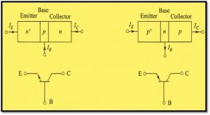
The diagrammatic representations of n-p-n transistors are given below.

NPN Transistor as diode connection
Diagram 2
3
NPN Transistor

The NPN transistor’s equivalent circuit.

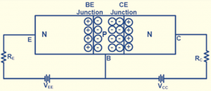
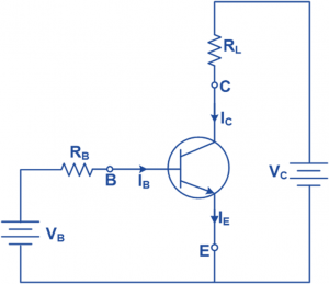
We can say that the working of a n-p-n transistor is similar to the working of 2 p-n junction diode connected one after another. These PN junction diodes are termed as the collector-base C-B junction and base-emitter B-E junction.

Consideration as per Doping:

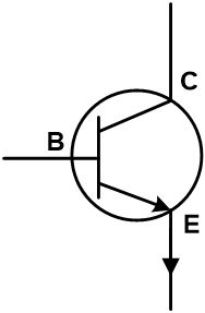
  • The emitter section is heavily doping section. The general rule is to keep the base’s width minimum among all the three terminals. As emitter is heavily doped, it can shoot up charge carriers to the base regions.
  • As mentioned earlier, the base has the minimum width and it also has the minimum doping. The base passes numerous charge carriers to the collector, which is carried from the emitter.
  • The collector regions is in comparison moderately doped and used for collecting charges from the base region.

NPN Transistor Symbol

NPN Transistor Symbol

NPN Transistor Pinout

As mentioned earlier, a transistor has three terminals. They are – Base, collector, and emitter.

How to identify NPN Pin?

  • In the majority of the configurations, the center part is for the base terminal.
  • The pin that is below this is a collector, and also, the rest of one is the emitter pin.
  • When the dot isn’t marked, all terminals has to be identified using there orientation or uneven terminal space between pin. Here the center pin is the base. The nearest pin is the emitter, and the rest pin is a collector terminal.

Applications of NPN transistors:

  • Usually, the NPN transistor is used as bipolar transistor because of electrons’ mobility, as it is higher than the mobility of holes.
  • These are also used in amplifying and switching the signals. These are used in amplifier circuits i.e., push-pull amplifier circuits.
  • The NPN transistor is used Darlington pair circuits to amplify weak signals to significantly scaling up signal.
  • If there is a need to sink current, then also NPN transistors could be used.
  • Other than these, NPN transistor has many applications in temperature sensors, circuits like logarithmic converters, etc.

How Does an NPN Transistor Work?

NPN transistor needs both the reverse and forward bias for working. The forward bias is established between the Emitter voltage and the emitter. The reverse bias is connected between the collector voltage and the collector.

5

Now, as the n side of a diode has electrons as majority and p side has holes as majority, all the voltage connections get arranged as forward and reverse bias accordingly. The base emitter junction is set as the reverse bias and the collector base junction works as forward bias. The depletion region of this emitter-base area is narrower compared to the depletion area of the collector-base intersection.

As the junction is reverse biased (emitter), the holes flow from the supply to the N junction. Then the electron moves towards the p side. Here, neutralization of some electron occurs. The rest of the electrons move towards the n-side. The voltage drop in respect to the emitter and base is VBE as input side.

In N-type emitters, the charge carrier is mostly electrons. Hence, electrons carried through N-type emitters to a P-type base. A current will be carried through the emitter-base or E-B junction. This current is known as the emitter current (Ie). Here the emitter current (IE) flows from output side and it flows in two directions; one is IB and other is IC. So we can write,

            IE=IB+IC

However, the base area is relatively thin and lightly doped. Hence, mostly electrons will pass the base area, and only few will recombine with available holes. The base current is minimum in comparison with emitter current. Usually, it’s up to 5% of the entire emitter current.

The current flowing from the rest of the electrons is referred to as the collector current (IC). The IC is comparatively high when compared with the base (IB).

N-P-N Transistor Circuit

The voltage source is connected to the NPN transistor. The collector terminal is joined to the +ve terminal of supply voltage (VCC) using a load resistance (RL). The load resistance can also be utilized to decrease the most current flowing through the circuit.

The base terminal is joined to the +ve terminal of the base provide voltage (VB) with resistance RB. The base resistance is used to restrict the maximum base current (IB).

When the transistor is ON operation, large collector current passing through the circuit between the collector and from the emitter. However, for that little quantity of base current must flowing to the bottom terminal of the transistor.

NPN Transistor Circuit

The markings represents the typical currents of Collector, bas and emitter.

Advantages and Disadvantages of using a NPN Transistor:

Advantages:

  • Small in size.
  • Can work in low voltage.
  • Very cheap.
  • Low output impedance.
  • Long lasting.
  • Spontaneous actions.

Disadvantages:

  • High Temperature sensitivity.
  • Produce low energy and power.
  • Can get damaged during a thermal runaway.
  • Cannot be operated in high frequencies.

NPN Transistor Switch

The transistor operates

  • Switched ON in the saturation mode
  • Switched OFF in the cut-off mode.

Switched ON in the saturation mode

  • When both junctions are in the forward bias condition, sufficiently high voltage is applied to input voltage. Hence, the transistor functions as a short circuit as VCE is approximately zero.
  • At that time two junctions are in the forward bias state, adequate voltage is in the input.
  • In this state, the current will pass between collector and emitter. The current is flowing within circuit.

Switched OFF in the cut-off mode.

  • If the two junctions of the transistors are in reverse bias, the transistor goes into OFF state.
  • During this mode of operation, the input signal voltage or the base voltage is zero.
  • Consequently, the total VCC voltage acts across the collector.

Operating Mode of Transistor

It has three modes of operation as per biasing, are as follows:

  • Active mode
  • Cut-off mode
  • Saturation mode

Cut-off Mode

  • The transistor acts as an open circuit.
  • In cut-off, the two junctions are in reverse bias.
  • The current won’t be allowed to flow through.

Saturation Mode

  • The transistor perform as a close circuitry.
  • Both junctions are configured in forward bias only.
  • As the base-emitter voltage is comparatively high a current pass from collector to emitter.

Active Mode

  • In this time, the transistor functions as a current amplifier circuit.
  • In the transistor’s active mode, the B-E junction is at forward bias, and the C -B junction is at reverse biased.
  • The current passes in between emitter and collector and the quantity of current are proportional to the applied base present.

To know more about electronics click here