Avalanche Photodiode Definition
Avalanche photodiodes or APDs are highly sensitive semiconductor devices that transform optical signals into electrical signals. These are operated under high reverse bias. The term ‘avalanche’ comes from the avalanche breakdown phenomenon.
Avalanche Photodiode Symbol

The symbol of avalanche photodiode is the same as that of Zener diode.
Avalanche Photodiode structure

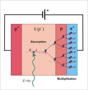
The structure of the ordinary Avalanche photodiode is similar to the PIN photodiode. It consists of two heavily doped (p+ and n+ region) and two lightly doped (I or intrinsic region and P region) regions. The width of the depletion layer in the intrinsic region is relatively thinner in APD than the PIN photodiode. The p+ region acts like the anode, and n+ acts like the cathode. Reverse bias is mostly applied across the pn+ region.
Avalanche photodiode Circuit Diagram

For applying reverse bias conditions, the p+ region is connected to the negative terminal, and the n+ region is connected to the battery’s positive terminal.
Avalanche photodiode working principle

- Avalanche breakdown takes place when the diode is subjected to high reverse voltage.
- The reverse bias voltage increases the electric field across the depletion layer.
- Incident light enters the p+ region and further gets absorbed in the highly resistive p region. Here electron-hole pairs are produced.
- A comparatively weaker electric field causes separation between these pairs. Electrons and holes drift with their saturation velocity towards the pn+ region where a high electric field exists.
- As the velocity is maximum, the carriers collide with other atoms and generate new electron-hole pairs. A large number of e-h pairs results in high photocurrent.
Avalanche photodiode Characteristics
- The intrinsic region in APD is slightly p-type doped. It is also called ?-region.
- The n+ region is thinnest, and it is illuminated through a window.
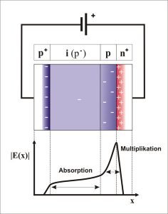
- The electric field is maximum at the pn+ junction, and then it starts decreasing through the p region. Its intensity lessens in ?-region and gradually vanishes at the end of the p+ layer.
- Even a single photon absorbed leads to the generation of a vast number of electron-hole pairs. This is called the internal gain process.
- Excess electron-hole pair generation due to the collision of charge carriers is called avalanche multiplication. Multiplication factor or gain,
M=Iph/Ipho
Where iph= multiplied APD photocurrent
ipho=photocurrent before multiplication
M value strongly depends upon reverse bias and temperature also.
Avalanche Photodiode Operation
APDs are operated in completely depleted mode. Besides the linear avalanche mode, APDs can also work in the Geiger mode. In this mode of operation, the photodiode is operated at a voltage above breakdown voltage. Recently another mode has been introduced, which is called Sub-Geiger mode. Here along with single-photon sensitivity, the internal gain is also very high, just below the breakdown.
Impact ionization in Avalanche Photodiodes
After the photons are absorbed in ?-layer, a sufficient number of electron-hole pairs are formed. The electric field separates the pairs, and the independent charge carriers run towards the n+ and p+ regions. In the p region, the electrons experience a massive electric field. In the effect of this field, electrons drift with their saturation velocity and collide. This collision helps in charge multiplication. This overall phenomenon is called impact ionization.
Ionization rate, k=α/β
Where ⍺= rate of electrons
ꞵ= rate of holes
Avalanche Photodiode Diagram

Avalanche Photodiode Datasheet
| Photodetector | Wavelength | Responsivity | Dark Current |
| InGaAs APD | 1310-1550 nm | 0.8 A/W | 30 nA |
| Germanium APD | 1000-1500 nm | 0.7 A/W | 1000 nA |
Avalanche Photodiode Module
APDs are part of modules that contain additional electronic elements apart from the photodiode. There can be a trans-impedance op-amp in some packages that improve the performance and increases bandwidth and responsivity. Some packages are optimized to be used in optical fiber. Some incorporate thermosensors to provide better stability.
Avalanche Photodiode Array
Avalanche photodiode arrays are small in size and also yield lease gain. These are designed especially for use in LIDAR, laser rangefinders, etc. Although APD arrays are not mainstream products yet, some manufacturers are making these due to their unique features.
Avalanche Photodiode Noise
The primary components of noise in APD are
- Quantum or shot noise (iQ): The avalanche process is the primary reason behind this.
- Dark current noise: Dark current noise is generated from the absence of light in a photodiode. It can further be classified into bulk current noise(iDB) and surface current noise(iDS).
- Thermal noise: It is the noise of the amplifier connected to the photodiode.
Due to carrier multiplication, significant noise is added to the existing noises. It is known as excess noise factor or ENF.
ENF or F(M)= kM + (2-1/M)(1-k)
Where M = multiplication factor
k = impact ionization coefficient
Therefore the mean square value of total noise iN in APD is,

Where
q= charge of an electron
Ip= photocurrent
B= bandwidth
M= multiplication factor
ID= bulk dark current
IL= surface leakage current
Thermal noise in trans-impedance amplifier is,

Where kB= Boltzmann constant
T= absolute temperature
RL= load resistance
Difference Between PIN and Avalanche Photodiode | Avalanche Photodiode vs. PIN Photodiode
| Avalanche Photodiode | Parameters | PIN Photodiode |
| Four layers- P+, I, P, N+ | Layers | Three layers- P+, I, N+ |
| Very high | Response time | Very less |
| Low value of current | Output current | Carrier multiplication causes amplified current value |
| Gain can be as high as 200 | Internal gain | Gain is insignificant |
| Highly sensitive | Sensitivity | Slightly less sensitive |
| Amplifiers can improve the performance, but APD can still function without this as the gain is already there. | Amplifier | No internal gain is there, so the use of amplifiers is mandatory. |
| Higher due to charge multiplication | Noise | Comparatively lesser than APDs |
| Extremely high | Reverse Bias voltage | Low |
| Great | Temperature stability | Poor |
Avalanche Photodiode Amplifier
Like PIN photodiodes, APDs also use the four-channel trans-impedance amplifier for reduced noise, high impedance, and low power consumption. Some amplifiers offer temperature flexibility and high reliability also. All these characteristics make the photodiode suitable for use in LIDAR receivers.
Avalanche Photodiode detector
APDs are preferred over PIN photodiodes in light detection for their increased sensitivity. As a relatively high voltage is given, the number of charge carriers overgrows, and they are accelerated in the effect of strong electric fields. The internal collision occurs, and charge multiplication takes place. As a result, the photocurrent value rises, which improves the overall photo-detection process.
Avalanche Photodiode in optical fiber communication
In optical fiber communication systems, APDs are usually needed for the detection of weak signals. Circuitry must be optimized enough to detect the weak signals maintaining a high SNR(Signal to noise ratio). Here,
SNR=(power from the photocurrent/power of photodetector) + power of amplifier noise
For achieving a good SNR, quantum efficiency must be high. As this value is nearly close to the maximum value, most of the signals are detected.
Comparison between APD and PMT | Avalanche Photodiode vs Photomultiplier tube
| Avalanche Photodiode | Photomultiplier Tube |
| It consists of four layers with different doping concentrations. | It consists of a photocathode, dynodes, and a vacuum glass tube. |
| It uses the avalanche multiplication phenomenon to produce charge carriers. | It uses the photon absorption technique for the emission of excess electrons. |
| It converts photons into electrons. | It amplifies the number of electrons. |
| APDs are highly sensitive. | The sensitivity of PMT is limited. |
| The cost of APDs is lower than that of PMTs. | PMTs are the costliest devices. |
APDs and quenching circuits
- Passive quenching circuit: This type of circuit uses a load resistor, a passive element, to quench the breakdown pulse. Photoelectrons trigger the avalanche. A large current is passed through the circuit to avoid the shortage of electrons or holes in the avalanche region, and the diode remains in conducting state.
- Active quenching circuit: While the diodes are recharged, the probability of another photoelectron striking it is very low. To minimize the dead-time, ‘active quenching’ is done. The bias voltage is temporarily dropped, and this delay allows the collection of all electrons and holes. When again the voltage is increased, no electron remains at the depletion region.
InGaAs Avalanche Photodiode
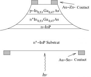
InGaAs or Indium Gallium Arsenide is vividly used in semiconductor devices. InGaAs avalanche photodiodes are used for achieving long-reach optical fiber communications. These can perform photo-detection in the range of 1100-1700 nm. InGaAs avalanche photodiodes are better than ordinary germanium avalanche photo diodes in terms of SNR and sensitivity.
Large area avalanche photodiode
Large area APDs or LAAPDs are lightweight photodiodes that possess a large activation area. Its features include fast response time, improved SNR, insensitivity to magnetic fields, etc.
Ultraviolet–UV Avalanche photodiode
Ultraviolet avalanche photo diodes offer outstanding sensitivity if operated in Geiger mode. The silicon carbide UV APD shows a high signal gain and extreme sensitivity. UV APDs are ideal for ultraviolet flame detection.
Silicon Avalanche Photodiode
High silicon APDs are great for low light detection. Internal multiplication features great photosensitivity that makes it capable of detecting low light signals. It also has improved linearity, low terminal capacitance, and low-temperature coefficient. Some applications of Si avalanche photo diodes are optical rangefinders, laser radars, FSO, etc.
Silicon Avalanche Photodiode array
In multi-element silicon APDs, the depletion region is fabricated just below the photosensitive area. Due to this, the APD array multiplies the incident light. The charge carriers struck in the depletion region. This implies that Si avalanche photo diode arrays have low crosstalk because of the gain.
Geiger mode avalanche photodiode
Geiger mode avalanche photo diodes are developed to provide an alternative to the photomultiplier tubes. GAPDs use the single-photon counting principle at a voltage little more than the threshold breakdown voltage. At this voltage, even a single electron-hole pair is capable of triggering a strong avalanche. In this situation, the quenching circuits reduce the voltage by a fraction of a second. This stops the avalanche for the time being, and photo-detection is possible.
Photon counting techniques with silicon avalanche photodiodes
Over the years, two types of photon counting techniques are being used in avalanche photo diodes.
- Geiger mode
- Sub-geiger mode
Studies suggest that the Geiger mode improves the performance excellently for using quenching circuits.
Single photon avalanche photodiode | Single Photon counting Avalanche Photodiode
These are also called SAPD. SAPDs are highly photosensitive and optimized for high quantum frequency. Some of its applications include an image sensor, 3D imaging, quantum cryptography, etc.
Advantages and Disadvantages of Avalanche Photodiode
Advantages of Avalanche Photodiode
- It can detect light of low intensity.
- Sensitivity is high.
- Response time is faster.
- A single photon can generate a large number of electron-hole pairs.
Disadvantages of Avalanche Photodiode
- High operating voltage is required.
- Excess noise due to carrier multiplication.
- Output is not linear.
Application of Avalanche Photodiode
- LASER scanner.
- Barcode reader.
- laser Rangefinders.
- Speed gun.
- Laser microscopy.
- PET scanner.
- Antenna Analyzer bridge.
FAQs
What is the response time of avalanche photodiode?
The average response time of different avalanche photo diodes can range from 30 ps to 2 ms.
What happens when you send too much light to an avalanche photodiode (APD)?
Too much exposure to light overheats the diode and may damage the device.
How does an avalanche photodiode work?
Avalanche photodiode utilizes the avalanche breakdown voltage to multiply charge carriers and increase current.
What is the difference between PIN photodiode and avalanche photodiode?
Avalanche photodiodes have four layers, and PIN photodiodes have three layers. Also, unlike PIN photo diodes, APDs have heavy internal gain and photosensitivity due to charge multiplication.
What are the drawbacks of avalanche photo diode?
APDs are susceptible to high noise due to impact ionization, and the output is non-linear. Other limitations has been discussed in “disadvantages of Avalanche Photo-diodes” section.
What is the primary advantage of an avalanche photodiode?
The primary advantage of the avalanche photo-diode is its sensitivity and ability to detect low-light signals.
What is the temperature effect on avalanche gain?
Gain varies linearly with temperature as reverse breakdown voltage has a linear relationship with temperature.
Why does avalanche breakdown increase with temperature?
A rise in temperature increases the vibration of atoms and decreases the mean free path. Since the path becomes smaller, charge carriers need more energy to travel. Therefore, the breakdown voltage needs to be increased.
For more electronics related article click here

Hi……I am Kaushikee Banerjee completed my master’s in Electronics and Communications. I am an electronics enthusiast and am currently devoted to the field of Electronics and Communications. My interest lies in exploring cutting-edge technologies. I’m an enthusiastic learner and I tinker around with open-source electronics.