Contents
- What is Integrator?
- Working principle of Integrator
- Op-amp integrator circuit
- Output of an integrator
- Derivation of Op-amp as integrator
- Practical op-amp integrator
- Applications of integrator
- What is Differentiator ?
- Op-amp as Differentiator
- Working Principle of Differentiator
- Output waveform of a differentiator
- Applications of Differentiator
What is Integrator?
Definition of Integrator
If the feedback path is made through a capacitor instead of a resistance , an RC Network has been established across the operational amplifiers’ negative feedback path. This kind of circuit configuration producing helps in implementing mathematical operation, specifically integration, and this operational amplifier circuit is known as an Operational amplifier Integrator circuit.
The output of the circuit is the integration of the applied input voltage with time.
Integrator circuits are basically inverting operational amplifiers (they work in inverting op-amp configuration, with suitable capacitors and resistors), which generally produce a triangular wave output from a square wave input. Hence, they are also used for creating triangular pulses.
Op-amp as Integrator
Working principle of Integrator
Operational amplifiers can be used for mathematical applications such as Integration and Differentiation by implementing specific op-amp configurations.
When the feedback path is made through a capacitor instead of a resistance , an RC Network has been established across the operational amplifiers’ negative feedback path. This kind of circuit configuration producing helps in implementing mathematical operation, specifically integration, and this operational amplifier circuit is known as an Operational amplifier Integrator circuit. The output of the circuit is the integration of the applied input voltage with time.
Op-amp integrator circuit
Output of an integrator
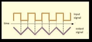
Integrator circuits are basically inverting operational amplifiers (they work in inverting op-amp configuration, with suitable capacitors and resistors), which generally produce a triangular wave output from a square wave input. Hence, they are also used for creating triangular pulses.
The current in the feedback path is involved in the charging and discharging of the capacitor; therefore, the magnitude of the output signal is dependent on the amount of time a voltage is present (applied) at the input terminal of the circuit.
Derivation of Op-amp as integrator
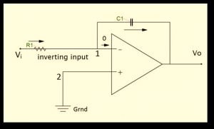
As we know from the virtual ground concept, the voltage at point 1 is 0V. Hence, the capacitor is present between the terminals, one having zero potential and other at potential V0. When a constant voltage is applied at the input, it outcomes in a linearly increasing voltage (positive or negative as per the sign of the input signal) at the output whose rate of change is proportional to the value of the applied input voltage.
From the above circuitry it is observed, V1 = V2 = 0
The input current as:

Due to the op-amp characteristics (the input impedance of the op-amp is infinite) as the input current to the input of an op-amp is ideally zero. Therefore the current passing from the input resistor by applied input voltage Vi has flown along the feedback path into the capacitor C1.
Therefore the current from the output side can also be expressed as:

Equating the above equations we get,

Therefore the op-amp output of this integrator circuit is:

As a consequence the circuit has a gain constant of -1/RC. The negative sign point toward an 180o phase shift.
Practical op-amp as aintegrator
If we apply a sine wave input signal to the integrator, the integrator allows low-frequency signals to pass while attenuates the high frequencies parts of the signal. Hence, it behaves like a low-pass filter rather than an integrator.
The practical integrator still has other limitations too. Unlike ideal op-amps, practical op-amps have a finite open-loop gain, finite input impedance, an input offset voltage, and an input bias current. This deviation from an ideal op-amp can affect working in several ways. For example, if Vin = 0, current passes through the capacitor due to the presence of both output offset voltage and input bias current. This causes the drifting of the output voltage over time till the op-amp saturates. If the input voltage current is zero in case of the ideal op-amp, then no drift should be present, but it is not true for the practical case.
To nullify the effect caused due to the input bias current, we have to modify the circuit such that Rom = R1||RF||RL
In this case, the error voltage will be

Therefore the same voltage drop appears at both the positive and negative terminals because of the input bias current.
For an ideal op-amp operating in the dc state, the capacitor performs as an open circuit, and hence, the gain of the circuit is infinite. To overcome this, a high resistance value resistor RF is connected in parallel with the capacitor in the feedback path. Because of this, the gain of the circuit is limited to a finite value (effectively small) and hence gets a small voltage error.

- VIOS refers to the input offset voltage
- IBI refers to the input bias current
What is Differentiator ?
Definition of Differentiator
If the input resistance in the inverting terminal is replaced by a capacitor, an RC Network has been established across the operational amplifiers’ negative feedback path. This kind of circuit configuration helps in implementing differentiation of the input voltage, and this operational amplifier circuit configuration is known as an Operational amplifier differentiator circuit.
An operational amplifier differentiator basically works as a high pass filter and, the amplitude of the output voltage produced by the differentiator is proportionate to the change of the applied input voltage.
Op-amp as a Differentiator
As we have studied earlier in the integrator circuit, op-amps can be used for implementing different mathematical applications. Here we will be studying the differential op-amp configuration in detail. The differentiator amplifier is also used for creating wave shapes and also in frequency modulators.
An operational amplifier differentiator basically works as a high pass filter and, the amplitude of the output voltage produced by the differentiator is proportionate to the change of the applied input voltage.
Working Principle of Differentiator
When the input resistance in the inverting terminal is replaced by a capacitor, an RC Network has been established across the operational amplifiers’ negative feedback path. This kind of circuit configuration helps in implementing differentiation of the input voltage, and this operational amplifier circuit configuration is known as an Operational amplifier differentiator circuit.
In a differentiating op-amp circuit, the output of the circuit is the differentiation of the input voltage applied to the op-amp with respect to time. Therefore the op-amp differentiator works in an inverting amplifier configuration, which causes the output to be 180 degrees out of phase with the input. Differentiating op-amp configuration generally responds to triangular or rectangular input waveforms.
A Differentiator Circuit
As shown in the figure, a connection of capacitor in series with the input voltage source has been made. The input capacitor C1 is initially uncharged and hence operate as an open-circuit. The non-inverting terminal of the amplifier is connected to the ground, whereas the inverting input terminal is through the negative feedback resistor Rf and connected to output terminal.
Due to the ideal op-amp characteristics (the input impedance of the op-amp is infinite) as the input current, I to the input of an op-amp is ideally zero. Therefore the current flowing through the capacitor (in this configuration, the input resistance is replaced by a capacitor) due to the applied input voltage Vin flows along the feedback path through the feedback resistor Rf.
As observed from the figure, point X is virtually grounded (according to the virtual ground concept) because the non-inverting input terminal is grounded (point Y is at ground potential i.e., 0V).
Consequently, Vx = Vy = 0
With respect to the input side capacitor, the current carrying through the capacitor can be written as:

With respect to the output side feedback resistor, the current flowing through it can be represented as:

From the above equations when we equate the currents in both the results we get,


The differentiating amplifier circuit requires a very small time constant for its application (differentiation), and hence it is one of its main advantages.
The product value C1Rf is known as differentiator’s time constant, and output of the differentiator is C1Rf times the differentiation of Vin signal. The -ve sign in the equation refers that the output is 180o difference in phase with reference to the input.
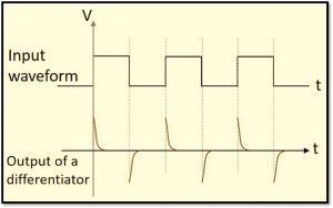
When we apply a constant voltage with one step change at t=0 like a step signal in the input terminal of the differentiator, the output should be ideally zero as the differentiation of constant is zero. But in practice, the output is not exactly zero because the constant input wave takes some amount of time to step from 0 volts to some Vmax volts. Therefore the output waveform appears to have a spike at time t=0.
Therefore for a square wave input, we get something like shown in the below figure,

For more Electronics related article and their detail explanation click here
.
Hi, I am Amrit Shaw. I have done Master in Electronics.
I always like to explore new inventions in the field of Electronics.
I personally believe that learning is more enthusiastic when learnt with creativity.
Apart from this, I like to strum Guitar and travel.


