Content: Master Slave Flip Flop
Master Slave Flip Flop Definition
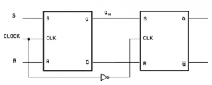
Master-slave is a combination of two flip-flops connected in series, where one acts as a master and another act as a slave. Each flip-flop is connected to a clock pulse complementary to each other, i.e., if the clock pulse is in high state, the master flip-flop is in enable state, and the slave flip-flop is in disable state, and if clock pulse is low state, the master flip-flop is in disable state, and the slave flip flop is enable state.
Master Slave Flip Flop is also Referred to as.
Pulse-triggered flip flop because the flip-flop can enabled or disabled by a CLK pulse during this mode of operation.
Master Slave Flip Flop Diagram
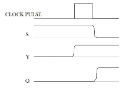
Assume that in the initial state Y=0 and Q=0, the next input is S=1 and R=0; during that transition, the master flip-flop is set and Y=1, there is no change in slave flip-flop as slave flip-flop is disabled by the inverted clock pulse, when the clock pulse of master changes to ‘0’, then the information of Y passes through slave and Q=1, in this clock pulse the slave flip-flop is active and master flip-flop gates deactivated.
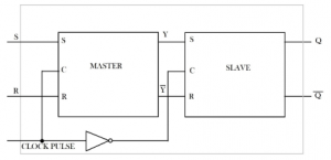
Master Slave Flip Flop Circuit | Master Slave Flip Flop Circuit Diagram
Master Slave Flip Flop Timing Diagram
The changes in input and output with respect to time can be defined in the timing diagram.
The behaviour of a master-slave flip flop can be determined through a timing diagram. For example, in the given figure below, we can see a signal of the clock pulse, S is the input signal to the master flip flop, Y is the O/P signal of the master flip flop, and Q is the output signal of slave flip flop.
Master Slave Flip Flop Truth Table
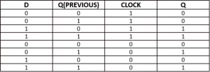
The truth table is a description of all possible output with all possible input combinations. In the master slave flip flop, there are two flip flops connected with inverted clock pulse to each other, so in the master slave truth table in addition to flip flop states, there must be an additional column for clock pulse so that the relationship between the input and output with the clock pulse can be determined.
Application of Master Slave Flip Flop
Mater slave configuration is mainly used to eliminate the race around the condition and get rid of unstable oscillation in the flip flop.
Advantages of Master Slave Flip Flop
Master slave can be operated on level triggered or edge triggered clock pulse; it can be used in various ways.
- A sequential circuit with an edge-controlled flip flop is straightforward to design rather than a level-triggered flip flop.
- By using the Master slave configuration, we also can eliminate the race around the condition.
Master Slave JK Flip Flop
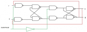
Master slave JK flip-flop could have been designed utilizing 2 JK flip-flops, in that each flip-flop is connected to CLK pulse complementary to each other, and the first flip flop is the master flip-flop which works when the CLK pulse is high state. And at that time the slave flip flop is in the hold state and if the CLK pulse is low state, then the slave flip-flop works, and the master flip-flop stays in the hold state.
The JK flip-flop characteristic is more or less similar to the SR flip-flop, but in SR flip flop, there is one uncertain output state when the S=1 and R =1, but in JK flip flop, when the J=1 and K=1, the flip flop toggles, that means the output state changes from its previous state.
JK Master Slave Flip Flop Circuit Diagram
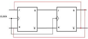
JK Flip Flop Master Slave Timing Diagram
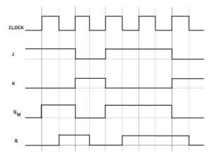
Master Slave JK Flip Flop truth table
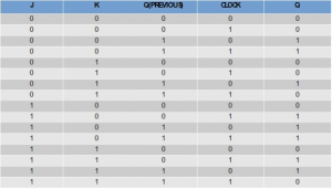
Master Slave JK Flip Flop Working
A master slave flip flop can be edge-triggered or level-triggered, which means it can either change its output state when there is a transition from one state to another, i.e., edge-triggered. The output of the flip flop changes at high or low input, i.e., level triggered. Master-slave JK flip flop can be used in both triggered ways; in edge-triggered, it can be +ve edge-triggered or -ve edge triggered.
In edge-triggered, the master flip flop is derived from the +ve edge of the clock pulse. At that time, the slave flip flop is in the hold state, i.e., the output of the master is according to its input. When the negative clock pulse arrived, the slave flip flop is activated. The o/p of the master flip-flop propagates through the slave flip-flop; at that time the master flip-flop is in the hold state.
Working:
- When J = 0, K = 0, there will be no change in the output with or without clock pulse.
- When J = 1, K = 0, and clock pulse is on positive edge, the output of master flip flop Q is set as high, and when the negative edge of the clock arrives, the output of master flip flop passes through the slave flip flop and produce output.
- When J = 0, K = 1, and clock pulse is one positive edge, the output of master flip flop Q is set as low and Q’ is set as high, when the negative clock edge arrives the Q’ output of the master flip flop feed into the slave flip flop, and that causes to set the output of the slave Q as low.
- When J = K = 1, then at the positive edge of the clock pulse, the master flip flop toggles (means the change of the previous state into its opposite state), and at the negative edge of the clock pulse, the slave flip flop toggles.
Master Slave JK Flip Flop Verilog Code
module jk_master_slave(q, qbar, clk, j, k);
output q, qbar;
input j, k, clk;
wire qm, qmbar, clkbar;
not(clkbar, clk);
jkff master(qm, qmbar, clk, j, k);
jkff slave(q, qbar, clkbar, qm, qmbar);
endmodule
module jkff(q, qbar, clk, j, k);
input j, k, clk;
output q, qbar;
always @(posedge clk)
 case({j,k})
  2'b00:
    begin
     q<=q;
     qbar<=qbar;
    end
  2'b01:
    begin
     q<=0;
     qbar<=1;
    end
  2'b10:
    begin
     q<=1;
     qbar<= 0;
    end
  2'b11:
    begin
     q<=~q;
     qbar<=~qbar;
    end
 endcase
endmodule
VHDL_code
library IEEE;
use IEEE.STD_LOGIC_1164.ALL;
entity jkff is
port(p, c, j, k, clk: in STD_LOGIC;
q,qbqr: out STD_LOGIC);
end jkff;
architecture Behavioral of jkff is
signal input: std_logic_vector(1 downto 0);
begin
input <= j & k;
process(clk, j, k, p, c)
variable temp: std_logic:=’0’;
begin
if(c=’1’ and p=’1’) then
if rising_edge(clk) then case input is
when “10” => temp:= ‘1’;
when “01”=> temp:= ‘0’;
when “11”=> temp:= not temp;
when other => null;
end case;
end if;
else
temp=’0’;
end if;
q<= temp;
qbar<= not temp;
end process;
end behavioral
Advantages of Master Slave JK Flip Flop
JK flip flop master slave over come the limitation of SR flip flop, in SR flip flop when S = R = 1 condition arrives the output become uncertain, but in JK master slave when J = K = 1, then the output toggles, the output of this state keep changing with the clock pulse.
Application of Master Slave JK Flip Flop
JK flip flop master slave overcome the limitation of SR flip flop, in SR flip flop when S = R = 1 condition arrives the output becomes uncertain. Still, in the JK master slave, when J = K = 1, then the output toggles, the output of this state keeps changing with the clock pulse.
Master Slave D Flip Flop
In this master slave also, two D flip flop connected to each other in series with clock pulse invited to each other. The basic mechanism of this master slave is also similar to other master slave flip-flops. D master slave flip flop can be level triggered, or edge triggered.
Master Slave D Flip Flop Circuit Diagram
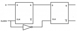
Fig. Block representation of master slave D flip flop circuit.
Master Slave D Flip Flop Timing Diagram
In the diagram, one signal of the clock pulse, one is D, the i/p to the master flip flop, Qm is the o/p of the master flip flop, and Q is the o/p of the slave flip flop.
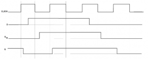
Fig. Master Slave D flip flop timing diagram
Master Slave D Flip Flop Truth Table
Master Slave D Flip Flop using NAND gates
The master slave D flip flop can be designed with NAND gates; in this circuit, there are two D flip flops, one is acting as a master flip flop, and the other is acting as a slave flip flop with an inverted clock pulse to each other. Here for inverter also NAND gats are used.

Fig. Circuit diagram of Master Slave D flip flop designed with NAND gates.
Master Slave edge triggered D Flip Flop
When the state of a flip-flop changes during the transition of a clock, the pulse is known as an edge-triggered flip-flop and these can be +ve edge-triggered, or -ve edge-triggered. The +ve Edge triggered flip flop means the state of it changed during the transition of the CLK pulse from ‘0’ to ‘1’ state. The –ve edge triggered flip flop implies the state of flip flop changes during the transition of the clock pulse from ‘1’ to ‘0’ state.

Fig. D- type positive edge master slave flip flop.
The positive edge triggered d master slave flip flop is designed with three basic flip- flop as shown in the above figure; S and R are maintained at logic ‘1’ for the output to remain steady. When S=0 and R=1, the output Q=1, where for S=1 and R=0 the output Q=0. When the clock pulse changes from 0 to 1, the value of D transferred to Q, change in D when the clock pulse is maintained at ‘1’ the value of Q does not get affected by it, and a transition from 1 to 0 also does not cause changes the output Q, nor when the clock pulse is ‘0’.
But in the practical circuit, there is a delay, so for proper output, we need to consider setup time and hold time for proper operation. A definite time before the clock pulse arrives, the requirement of the value of D should be assigned that time is called the setup time. Hold time is the time for which input should behold after the clock pulse arrives.
RS Master Slave Flip Flop
Master slave is a configuration to prevent the unstable behavior of a flip flop; Here in RS master slave flip flop, two RS flip flop are connected to form master slave configuration, here flip flop is connected to a clock pulse inverted to each other; when the positive half of the clock pulse arrives the master flip flop is activated, and during negative clock pulse the slave flip flop is activated. Each flip flop works at different time interval.
In master salve configuration of RS flip flop, an unsalable oscillation cannot take place, because at a time master flip flop is in hold state or the slave flip flop is in hold state. For proper working of mater salve flip flop, we must consider hold time and setup time which can vary from one circuit to another; it depends on the design of the circuit.
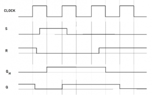
Master Slave SR Flip Flop Timing Diagram
Here, there is one clock signal, S is the input signal to the master flip flop, R is also an I/p signal to the master flip-flop, Qm is the O/P of the master flip-flop, Q if the O/P signal of the slave flip-flop.
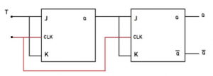
Master Slave T Flip Flop
FAQ/Short Notes
What do you mean by flip flop? | What is Flip Flop with example?
The flip flop is a fundamental element in the sequential logic circuit, a bi-stable element, as it has two stable states: ‘ 0,’ and the other is ‘1’. It can store only 1-bit at a time and a flip-flop circuit capable to maintain its state indefinitely or until when power is delivered to the circuit. The O/P state of the flip flop can be changed with input and clock pulse to the flip flop. When a latch circuit is added with some basic gates and clock pulse, it is a flip flop. Example of flip flop is D flip flop, SR flip flop, JK flip flop, etc.
What is S and R flip flop?
In a SR flip-flop, the S stands for the set and R stands for reset;because of this, it is also named as the Set Reset flip-flop. It can be designed with two AND gates and a clock pulse to an SR-latch. When the clock pulse is ‘0’, any input value through S or R cannot change the output value Q, and when the clock pulse is ‘1’, the value of output Q depends on the input values of S and R.

What are the types of flip flop?
There are four types of a flip flop:
- SR FFs.
- JK FFs.
- D FFs.
- T FFs.
What is a JK flip flop?
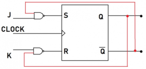
JK flip flop characteristic is more or less similar to the SR flip flop, but in SR flip flop, there is one uncertain output state when the S=1 and R =1, but in JK flip flop when the J=1 and K=1, the flip flop toggles, that means the output state changes from its previous state.
JK flip flop can be designed by adding AND gates to the input of S and R in SR flip flop, the input J and output Q’ is applied to the AND gate attached with S and input K, and the output Q is applied to the And gate connected to R.
How does JK flip flop works?
When the clock is not provided, or the clock is low, the input change cannot affect the output. So, for manipulation of output with the input clock, the pulse must be high.
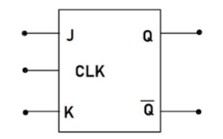
Working of JK flip flop when the clock pulse is high:
- When J = 0 and K = 0, there will be no change in the output.
- When J = 0 and K = 1, then the value of output will get reset.
- When J = 1 and K = 0, then the value of output will get set.
- When J = 1 and K = 1, the output value gets toggled (means to switch to the opposite state). In this state, the output will continuously change with the clock pulse.
Why JK flip flop is used?
JK flip flop is more versatile than D- flip flop or SR flip flop; they can operate more function than any other flip flop, they are widely used to store binary data. JK flip flop also overcome the uncertain states of SR flip flop.
How does JK flip flop toggle?
When the input to the flip flop J = K = 1 with clock pulse high, that’s when the JK flip flop toggles.
Why D flip flop is called delay?
The next output state of the D flip flop follows the input D, when the clock pulse is applied, in this way the input data is transfer to the output with delay, that’s why it is called a delay flip flop.
What are the applications of flip flop?
The flip flop is generally used as a
- The memory elements.
- In the shift-registers.
- The digital counters.
- The freq. Divider circuits.
- The bounce elimination switch, etc.
What are the characteristics of flip flop?
It is a synchronous sequential circuit; it changes its output state only when the clock pulse is present. It is the basic memory element for any sequential circuit, it can store one bit at a time. It is a bistable device.
What is the difference between D and T flip flop?
- D flip flop can not take similar input as D and D’ is its two input, so the input is always complementary to each other. On the other hand, Both the input in T is the only T so both inputs to the T flip flop will always be the same.
- D flip flop is a delay flip flop, in this flip flop, the output follows the input with the arrival of the clock pulse, whereas the T flip flop is called a Toggle flip flop, where the output changes to the opposite state with every arrival of the clock pulse when the input is 1.
Where are D flip flop used?
It is commonly used as a delay device or to store 1-bit data information.
I have graduated in Applied Electronics and Instrumentation Engineering. I’m a curious-minded person. I have an interest and expertise in subjects like Transducer, Industrial Instrumentation, Electronics, etc. I love to learn about scientific researches and inventions, and I believe that my knowledge in this field will contribute to my future endeavors.