CONTENTS
- What is CMOS image sensor ?
- Different types
- Working principle
- Designing
- Architecture
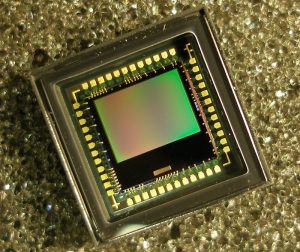
Cover Image By – Zach Dischner, Nerd-Tographer Desk Ornament (9698639550), CC BY 2.0
What is CMOS image sensor ?
CMOS Image and Colour Sensor:
Complementary metal-oxide semiconductor (CMOS) image sensors is comprised of photodiodes with and mixed-signal circuits ahving capability to amplify small photocurrents into digital signals. The CMOS image sensor is one of the best cricuitry for multiple photography related applications, i.e digital video cameras, photo scanners, Xerox machine, printing and various others. CMOS are nowadays utilized because of its multiple usage and it’s simple fabrications technique even with constain of sensivity in comparison with CCD.
Three types of the topology of CMOS colour sensors are discussed, namely the transimpedance amplifier (TIA), light to frequency converter, and light integrating.

Image Credit : Filya1, Matrixw, CC BY-SA 3.0
Working Principle of CMOS Image Sensor:
In general, four types of procedures are available
- Standard CMOS,
- Analog-mixed-signal CMOS,
- Digital CMOS, and
- CMOS image sensor processes.
The most obvious difference between this process and the other processes is the availability of photo devices, such as a pinned photodiode. The advantages of smaller dimension technology are smaller pixel, high spatial resolution, and lower power consumption. A technology lower than 100 nm requires modification to the fabrication process (not following the digital road map) and pixel architecture.
Fundamental parameters such as leakage current (will affect the sensitivity to the light) and operation voltage (will affect dynamic range, i.e., the saturation, a pinned photodiode is most likely not going to work at a low voltage are very important when a process is selected for CIS development. Because of these limitations, a new circuit technique is introduced:
1. An old circuit, such as a standard pixel circuit cannot be used when using 0.1 micron and lower. This is due to the topology which requires high voltage; because the maximum supply voltage is now lower.
2. Calibration circuit and cancellation circuit are normally employed to reduce noises.
In order to increase the resolution into multi-megapixel and hundreds of frame rate, lower dimension technology is normally chosen. Evidently, it has been reported that 0.13 micron and 0.18 micron are good enough to achieve good imaging performance.
These modifications of the CMOS process have started at 0.25 micron and below to improve their imaging characteristics. As process scaling is going to be much lower than 0.25 micron and below, several fundamental parameters are degraded, namely, photo responsivity and dark current. Therefore, the modifications are focused on mitigating these parameter degradations. System requirements (such as supply voltage and temperature) are also one of the criteria in selecting a suitable process.
The price of tool and development costs will also determine the process selection.
Photo Detetor Devices
The typical photo detector devices are photodiode and phototransistor. Typical photodiode devices are N+/Psub, P+/N_well, N_well/Psub, and P+/N_well/Psub (back-to-back diode) [9]. Phototransistor devices are P+/n_well/Psub (vertical transistor), P+/N_well/P+ (lateral transistor), and N_well/gate (tied phototransistor).
These standard photo devices still require a micro lens and colour filter array. The quantum efficiency of photodiodes in a standard CMOS is usually below 0.3.
The devices which are normally developed for the modified CMOS process are a photogate, pinned photodiode, and amorphous silicon diode. These devices will improve the sensitivity of the CIS. A pinned photodiode, which has a low dark current, offers good imaging characteristics for the CIS.
The photodevices exhibit the parasitic capacitance, which should be considered during the design process. An example of the parasitic capacitance of N_well/Psub is:
Cphoto = (capacitance per area) × photodevice area.
Design Methodology of CMOS Image Sensors:
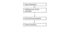
The typical design flow of the CMOS image sensor is shown below.

A wave propagation simulation can be done for optics simulation. Commercially available technology computer-aided design tools, such as from Synopsys and Silvaco, can be used to simulate the process or technology of the photodevices. There is a work, (mixed-mode simulation) that combines the technology computer-aided design and pixel-level simulation.
There are many electronic design automation tools available for pixel electrical simulation, these electronic design automation tools are similar to any integrated circuit (IC) design tool, such as spectre, SPICE, Verilog-A, and Verilog. These tools may be time consuming sometimes if the number of pixels is large.
Indeed, if large pixels together with the deep submicron process are required, more capital has to be provided (cost of tools are more expensive for very deep submicron, especially below 90 nm). Even though the CMOS foundry provides the models for supported design tools, sometimes designers still have to model the sub-block on their own to suit the CIS specification. This can speed up the pixel electrical simulation time, however, this will degrade the accuracy. For system simulation, VHDL-AMS, System-C, or MATLAB can be used to predict the overall function and performance.
CMOS Image Sensor Architecture:
Pixel Level ADC – A digital pixel sensor (DPS) offers a wide dynamic range. The DPS converts the analog values to a digital signa within the pixel range. The processing can also be done at the pixel level.

Chip Level ADC – Chip-level ADC or sometimes matrix-level ADC is depicted in Figure below.

The ADC for this topology has to be very fast, this topology would also consume a very high current. The ADC type suitable for the CIS topology is pipelined ADC. However, successive approximation register (SAR) and flash type ADC have also been reported in the CIS design. The balance of necessary overall power intake and speed of operation is therefore essential.
Digital Pixel Sensor – The DPS concept is similar to the solution used in the CMOS neuron-stimulus chip. The DPS in number is found useful for on-chip compression. The photodiode is used to discharge the input capacitance of the comparator and photodiode itself. It will be discharged proportionally to the light intensity. When this reaches the threshold, the comparator’s O/P will be triggered.
Low Power Technique in CMOS Image Sensor:
Biasing method: The subthreshold region or weak inversion biasing is one of the approaches to achieve low current consumption. This technique can be applied to an operational transconductance amplifier (OTA) or an amplifier for an ADC. Triode region biasing can also be used to further reduce power consumption.
Circuit technique: The regenerative latch can be used to reduce the digital power consumption. Reducing/scaling the capacitors in the pipeline stages (for ADC) can also reduce the power consumption.
Advanced power management technique: Another type of biasing or circuit technique, a “smart” approach, such as harvesting solar energy can also be employed to reduce the power consumption. We can also selectively ON only the required readout circuit. Pixels can also be periodically activated to reduce the power consumption further.
Low Noise Techniques in CMOS Image Sensor:
At pixel level: The thermal noise can be reduced by correlated double sampling and oversampling. The flicker noise is reduced by using a large device, periodically biasing the transistor, and proper PMOS substrate voltage biasing.
Column level: The off-chip calibration can be used to reduce fixed pattern noise. The calibration is done to select suitable capacitor weights in the SAR ADC.
ADC level: The kT/C noise is reduced by selecting a suitable value for Cf and Cs of the S/H circuit and buffer.
Photodiode level: The high conversion gain helps to reduce referred-to input noise.
For more electronics related article click here

Hi, I am Soumali Bhattacharya. I have done Master’s in Electronics.
I am currently invested in the field of Electronics and communication.
My articles are focused on the major areas of core electronics in a very simple yet informative approach.
I am a vivid learner and try to keep myself updated with all the latest technologies in the field of Electronics domains.
Let’s connect through LinkedIn –