Introduction to VLSI Design Flow
In the previous article, we have got an overview of VLSI design flow. In this article, we will learn about how different logic circuits can be implemented using VLSI design. VLSI is one of the key technologies in this era of digitalization. Transistors are used to implement logic circuits in VLSI design.
Digital logics are three types – the Inverter of the NOT gate, the AND gate, and the OR gate. More complex gates like -NAND, NOR, XNOR, and XOR can also be made using the basic gates. Let us discuss some of the methods of implementation of logic circuits.
CMOS Logic Design
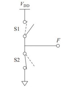
Digital is everything about ZERO and ONE or HIGH or LOW. The input for a digital logic circuit will be either 0 or 1, so as the output value. Now, if a circuit takes input as 0 and 1, then the logic can be understood by the switch function as given-below.

We can see in the image that when the s1 switch is opened and the s2 switch is closed, then the output will be 0; for vice versa, the output will be 1.


For Complete VHDL Tutorial! Click Here!
CMOS Design Methodology
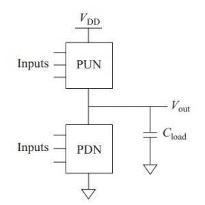
There are three steps for designing a CMOS logic as a part of VLSI design flow.
- Find out the complement of the Boolean Expression you need to implement.
- Describe the PUN
- Describe the PDN
The Pull Up Network Design:
Multiplying terms: NMOSFETs in parallel connection
Additive Terms: NMOSFETs in series connections
The Pull-Down Network Design:
Multiplying terms: NMOSFETs in series connections
Additive Terms: NMOSFETs in parallel connections
Design Your First VHDL Model using Xilinx. Click here for step by step guide!
CMOS Inverter / CMOS NOT Gate Design
A digital inverter is a NOT gate that gives the inverted output for an input. For high input or input is digital ONE, then the output is low or digital ZERO. For low input or input is digital ZERO, then the output is high or digital ONE.
| INPUT | OUTPUT |
| HIGH | LOW |
| LOW | HIGH |
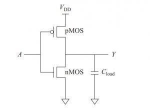
A CMOS inverter is made of two enhancement-mode transistors – one is NMOS, and the other is PMOS. The NMOS works as a pull-down network, and the PMOS works as a pull up network. The input voltage controls both the transistors.
When the PMOS transistor is in the ON state, the NMOS transistor goes into the OFF state. Also, when the NMOS transistor stays OFF, the PMOS will be in an ON state. That is how both the transistors work in complementary mode.
The transistor, which remains in OFF state, provides a high impedance value, and the output value changes. Under the same rail, a CMOS logic-circuit has less noise than an NMOS logic-circuit.
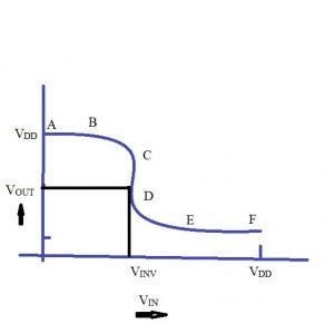
The graph of the voltage transfer characteristics of a symmetrical CMOS is given below.

Operation
The transistors are made in such a way that their threshold voltages should be of equal magnitude and opposite polarity. That is, the threshold voltage of NMOS will be equal to the magnitude of the threshold voltage of PMOS, given by the below expression.
VTN = – VTP
When the input voltage (Vin) is smaller than the threshold voltage of the NMOS transistor, then the NMOS transistor is in an OFF state. Then, the PMOS circuit will control the output voltage (Vout) with the supplied voltage (VDD). The AB region of the graph represents this operation.
Now, when the input voltage is greater than the difference of VDD and threshold voltage, then the PMOS logic circuit enters into an OFF state, and the NMOS gets activated. Then, NMOS controls the output voltage (Vout) with the ground voltage that is 0 V.
The graph’s BC region represents the saturated NMOS, and the CD part represents both the transistors are in saturated mode. VINV is the input voltage value for which the input voltage equals the output voltage.
From careful observation, we can say that the change is very high-pitched for the voltage swipe from 0 to VDD. That is why the CMOS inverter is a perfect inverter for logic design.
Now, when the input voltage is equal to the VINV, both the transistors are in saturation. The pull up network (PUN) will have VGS value =
VGS = Vin – VDD
Or, VGS = VINV – VDD
Current equation for saturation region is given as –
ID = μεW * (VGS – VTH )2 / 2 LD
This equation can be rewritten for pull up network–
IDpu = μpεWpu * (VINV – VDD – VTHP)2 / 2 D Lpu
The equation for pull down network will be –
IDpd = μnεWpd * (VINV – VTHN )2 / 2 D Lpd
Equating the drain current as per the characteristics –
μnεWpd * (VINV – VTHN )2 / 2 D Lpd = μpεWpu * (VINV – VDD – VTHP)2 / 2 D Lpu
or, VINV – VDD – VTHP = – β (VINV – VTHN) ; [ β = (μn * Zpu / μp * Zpd) ½]
Or, VINV = (VDD + VTHP + β * VTHN) / (1 + β)
If VTHN = – VTHP, then β comes as 1.
Furthermore, VINV comes as VDD/ 2 and
Zpd : Zpu = μn : μp =~ 2.5 :1
Power Dissipation
CMOS logic-circuits dissipate less power than that of an NMOS logic-circuit for low frequency. The CMOS power degeneracy swings as per the switching frequency of the circuit.
Noise margins
Noise margin is the maximum allowable deviation that can be occurred without changing the main feature under noisy conditions. NML is given as the difference between the logical threshold voltage and the logic ZERO equivalent voltage for a CMOS inverter of low level. The noise margin is described as the difference between the logic high or ONE equivalent voltage and the logical threshold voltage for the high level.
CMOS two input NAND and NOR gates
NOR and NAND gates are known as universal logic gates, which can be used to implement any logic equation or any kind of other logic gates. These are the two most manufactured gates using the CMOS logic for VLSI technology. Let us discuss the implementation and design of both the gates using CMOS logic.
CMOS NOR gate
A NOR gate can be described as an inverted OR gate. The truth table of the NOR gate is given below, where A and B are the inputs.

A NOR gate can also be implemented using CMOS technology. The CMOS inverter circuit comes into work in this design. A pull-down network (transistor) is added with the basic CMOS NOT gate in a parallel connection to implement the NOR operation. For two input NOR gates, only one pull-down network is added. To incorporate more numbers of inputs, more transistors are added.
Operation
The logic implementation using CMOS is shown in the below image. When any of the inputs is logic high or logic ONE, then the pull-down way to the ground is locked. The output will be logic ZERO.
When both the inputs get HIGH voltage or logic – ONE value, then the output value will be logic high or ONE. The logical threshold voltage will be equal to the threshold voltage of an inverter. That is how NOR logic can be achieved using CMOS.
CMOS NAND gate
A NAND gate can be described as an inverted AND gate. The truth table of the NAND gate is given below, where A and B are the inputs.

A NAND gate can also be implemented using CMOS technology. The CMOS inverter circuit also comes into work in this design. A pull-down network (transistor) in series and a depletion mode transistor are added with the basic CMOS NOT gate to implement the NAND operation. For two input NAND gates, only one transistor is added. To incorporate more numbers of inputs, more transistors are added to the series connection.
Operation
The logic implementation using CMOS is shown in the above image. When both the inputs are logic ZERO, both the NMOS transistors are in OFF state, while both the PMOS transistors are in ON state. The output gets connected to VDD, and that is how the output provides logic ONE or high value.
When input A gets a high value as input, and the input B gets a low value, the upside NMOS goes into ON state, and lower NMOS goes into OFF state. The ground connection cannot be established with the output value. In this condition, the left PMOS gets ON, whereas the right PMOS stays in the OFF state. The VDD finds a path through output and provides a high output value or logic 1.
When input B gets a high value as input, and input A gets a low value, the upside NMOS goes into OFF state, and lower NMOS goes into ON state. The ground connection cannot be established with the output value. Also, in this condition, the left PMOS gets OFF, whereas the right PMOS goes into the ON state. The VDD finds a path through output and provides a high output value or logic 1.
For the final logic, when both the input gets high input voltage or logic ONE value, both the NMOS transistors are in ON state. Both the PMOS transistors are in OFF state, providing a path for the ground voltage to connect with the output. The output thus provides logic ZERO or low value as output.
For more Electronics related article and VLSI design flow click here

Hi, I am Sudipta Roy. I have done B. Tech in Electronics. I am an electronics enthusiast and am currently devoted to the field of Electronics and Communications. I have a keen interest in exploring modern technologies such as AI & Machine Learning. My writings are devoted to providing accurate and updated data to all learners. Helping someone in gaining knowledge gives me immense pleasure.
Let’s connect through LinkedIn –