Contents of Photo diode detector
In this article we will discuss about photo diode detector as follows:
- Definition of a photodetector
- Different types
- Circuit Diagram
- Applications
- What is a Photodiode
- Features of a photodiode
- Working principle
- Avalanche photodiode
- Circuit Diagram
- Applications
- Advantages & disadvantages
- Phototransistor vs. photodiode
What is a Photo Detector?
Definition of a Photo Detector:
“Photodetectors are important elements, possess the ability to transform light into electrical signals.”
“Photodetectors are important elements useful in image processing, optical communication, security, and night vision and motion detection.”
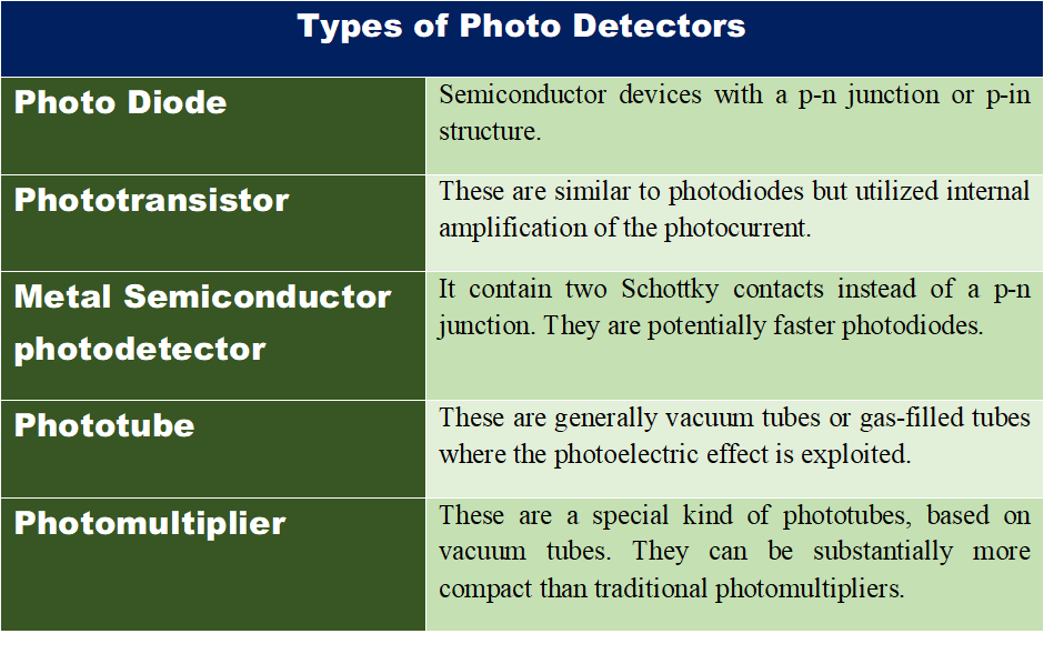
Types of Photo Detectors:

Important Applications of Photo Detectors:
- Photo Detectors can be employed for properties like optical power, luminous flux measurements.
- These are used in various types of optical-sensor and microscope design.
- Photo detectors are essential for laser rangefinders.
- Fast photodetectors are commonly utilized in optical-fiber communication, frequency metrology etc.
What is a Photo Diode?
Definition of a photodiode:
“A photodiode is basically a typically p-n junction diode.“
When a photon strikes the diode, it will excite electron and generates a moveable electron and a positive charge hole. The absorption happens in the junction’s depletion area, the carrier will removed from the junction by the depletion region’s built-in potential.
How does a photodiode work?
Working Principle of photodiode:
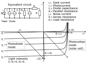
A photodiode is a p-n junction or a P-I-N configuration. If a photon strikes the diode, it produces the electron and a positively charged hole. When there’s any absorption happens in the juncture’s depletion area, these carriers have been trapped in the juncture from the built-in area of this depletion region that created a photocurrent.
Photodiodes are widely used under inverse biasing or without biasing. The light or photon can drive a current across this circuitry, which gives to the forward bias, which subsequently causes ‘Dark current’ from the reverse direction to the photocurrent. This is referred to as the natural effect and can be the foundation of solar cell design. A solar panel is just a combination of multiple effectual photodiodes.
Reverse bias produce minor current along exactly identical direction. Apart from that, the photodiode exhibits less noise.
Avalanche photodiodes have a similar prearrangement, but it’s normally operated with a greater reverse biasing. This enables every single photo-generated provider to be multiplied with avalanche breakdown, leading to photodiode’s internal effects and improves the device’s overall responsivity.
Materials for a photo diode:
Material used in photodiode:
- Silicon
- Germanium
- Lead Sulfide
The materials used for the construction of photodiode is important to describing its properties because only photons with appropriate energy can excite electrons in bandgap and able to produce substantial photocurrents.
It is important to remember that, silicon-based photodiode have greater band-gap and because of this it is capable to produce less noise than germanium-based photodiodes.
Since transistors and ICs are prepared by semiconductor material too and comprise p-n junctions, may act like a photodiode. This is not the accepted, an opaque housing is mandatory to remove this effect. Though these is not entirely opaque towards high energy radiations, may still cause ICs to malfunction for induced photocurrent.
Applications of a Photo Diode:
- Photodiodes are used in consumer electronic i.e., CD players, fire and smoke detectors, remote controls, lighting etc.
- These are also employed in various medical applications, detector and high-energy physics etc.
Advantages and Disadvantages of a Photo Diode:
ADVANTAGES-
- Low noise
- Low cost
- Compact and lightweight.
- Long Lifetime
- No high voltage is required.
- High quantum efficiency.
DISADVANTAGES-
- Small area
- No internal gain
- Much lower sensitivity
- Response time is slower.
What are the characteristics of a Photo Diode?
There are two types of characteristics of photo diode
- Electrical Characteristics
- Optical Characteristics
Electrical Characteristics of Photo Diode:

SHUNT RESISTANCE, RSH
Shunt Resistance (RSH) is used to estimate the thermal noise when no reverse bias is applied. It’s the ratio of voltage to current.
It is computed from the slope of the photodiode’s V-I curve at the origin.
SERIES RESISTANCE
Series resistance is give by Rs and it comes from the resistances of silicon. The expression is given by the following equation –

JUNCTION CAPACITANCE, (Cj)
Junction Capacitance (Cj) is the capacitance of the diode at a given reverse bias.
The junction capacitance is proportionate to the diffusion area and inversely proportionate to the width of depletion area.

RISE AND FALL TIME ( tr , tf )
The time taken to reach Ninety percent from ten percent is known as Rise Time and the time taken to fall from Ninety percent to Ten percent is known as Fall time. This parameter commonly expressed in frequency response of 3dB decay as follows.
tr=0.35/f3dB
BREAKDOWN VOLTAGE (VBR)
It is the max negative voltage which can be applied to the diode terminal.
NOISE EQUIVALENT POWER (NEP)
The photon intensity is prerequisite to equivalent the noise at a specified reverse biasing. It is a measurement of NEP.
RESPONSE TIME (tr)
It is defined by the time required for a diode to respond a step input in light at a specified reverse biasing mode of operation.
Short circuit current (ISC):
With the diode pins shorted, the current that flows at a given light intensity.
Optical Characteristics of Photo Diode:
QUANTUM EFFICIENCY, QE
QE is extensively recognized as the percentage of the incident photons that contribute to the photocurrent.
QE=R obs/R Id (100%)
RESPONSIVITY, R
The responsivity of a silicon photodiode is the measurement of the sensitivity to light. It is given by the ratio of Ip to the coming power of light (P) for the given wavelength.
R=IP/P at specific wavelength
NON-UNIFORMITY
It is well-defined as the variations of responsivity witnessed over the active photodiode surface area with a trivial spots of light.
NON-LINEARITY
A silicon photodiode characteristic is linear in nature though minor change in current regulates photocurrent linearity.
Noises in a Photo Diode:
In a photodiode, two types of noises are introduced; they are
- Shot Noise
- Johnson Noise.
Shot Noise
It is expressed by the following equation.

Thermal Noise or Johnson Noise
The photodetector may produce Johnson noise because of the thermal generation of carrier. The magnitude of this generated current noise is:

Hence, the total noise is,

Explain Avalanche and Zener Mechanisms:
Avalanche breakdown happens only at the higher voltages. Assume the electric field (E) in the transition region is enormous. Then, an e– incoming from the P side may get accelerated with kinetic energy to collide with the lattice and produce ionization. The interactions will create carrier multiplication; the original electron and generated electron are swept to the N side, and the create hole is flounced to the P. This process is Avalanche since each incoming carrier be able to initiate the large number of carriers.
Zener effect happens once tunneling of electrons take place from the P-side valance band to N-side conduction band, may causes reverse current flow from N to P terminal. Basic inevitabilities for tunneling current are a large number of electrons that are detached from a substantial quantity of unoccupied state by a tinny barrier. Since the tunneling probability be governed by the barrier width, doping must be great.
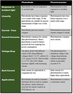
Compare between Photo Transistor and Photo Diode:

For more Electronics related article click here

Hi, I am Soumali Bhattacharya. I have done Master’s in Electronics.
I am currently invested in the field of Electronics and communication.
My articles are focused on the major areas of core electronics in a very simple yet informative approach.
I am a vivid learner and try to keep myself updated with all the latest technologies in the field of Electronics domains.
Let’s connect through LinkedIn –