Topic of Discussion: MOS Transistor
What is MOS Transistor?
A Metal-Oxide-Semiconductor or ‘MOS’ transistor is recognized for its operation as an ideal switch operation. A MOS transistor chip performs as a reliable current and capacitor of the transistors and its wires.

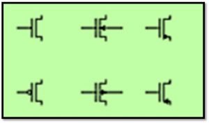
In the figure below, we can see some regular schematics of MOS transistors that are used commonly

We typically use the different terminal symbols i.e., figure when the body along with the substrate or the well-connection needs to be shown.
Working Principle of MOS Transistor:
For being a majority carrier device, a MOS transistor carries the current between its source and drain. This transistor gets regulated with a regular voltage applied to the gate of the respective MOS. In an n-MOS transistor, the electrons act as a the majority carrier while in a p-MOS type, Holes is acts as majority carriers. A MOS transistor is examined with an isolated MOS structure with a gate and body included to know about its properties or behavior’s figure below gives a simple structure of MOS. The top most layer of the MOS structure is made of a conductor.
This is very good for carrying currents for any charge; which is acknowledged as the gate. The transistors which were made at the very beginning, used metal gates; with the up growing time period, the transistor gates were changed and polysilicon is being used. The intermediate mid-layer of a MOS is made of a thin insulating film of silicon oxide which is usually identified as the gate oxide. The layer at the lower level is doped with silicone.
If we apply a negative voltage in the gate, a negative charge on the gate is produced. Beyond the gate, the holes are attracted toward the region as the mobility carriers are charged with positive energy. This is called the accumulation mode.
In figure (b), a A very minimal amount of voltage is supplied to the gate, which we get from a positive charge on the gate. To form a depletion region, the holes of the body which are generated from repulsion, get accumulated under the gate.
In figure (c), Threshold Voltage Vt is supplied and few electrons gets attached to that area.
Inversion Layer:
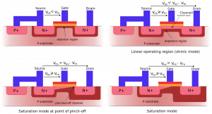
The conductive layer of the electrons in the p-type body is considered as an the ‘inversion layer’.
Here, the threshold voltage depends on two parameters, they are – 1. MOS’s dopants 2. Oxide layer’s thickness. It is regularly positive but they also can be made into negative ones. The nMOS transistor has piles of MOS between both the n-type regions called the source and the drain.
At this point, the gate-to-source voltage Vgs < the threshold voltage (Vt). The source and drain are having no of free electron in both sides. When the source is not working i.e., in ground state, the junctions are said to be reverse-biased, so no current flows. When the transistor is said to be OFF, this mode of operation is called cut-off.
the current is 0 if we compare it with an ON-transistor. The gate voltage is higher than the threshold voltage. Now if an inversion region of electrons which are the channel, makes a bridge between the source and drain and create a conductive path and turns the transistor ON. The increase in the number of total carriers and the conductivity increases are proportionate to each other with respect to the applied gate voltage.
The drain voltage – Source voltage is given as:
VDS = Vgs – Vgd . When, VDS = 0 (i.e., Vgs = Vgd),
there is no such electric field exists to produce current from drain to source.

When, The voltage (Vds ) is applied to the drain, and the current Ids carries through the channel of drain to the source. If Vds becomes larger than that Vgd < Vt, the channel doesn’t seem to have any change near the drain and hence it is in off state. Even after this, the conduction is being continued with the help of the drifted electron which is generated by the +ve voltage.
When the electrons reached to the termination of the channel, the depletion region adjoining the drain gets accelerated in the direction of it. The injected electrons accelerate this process.
Saturation Mode:
In this mode, the current Ids is controlled by the gate voltage and gets terminated by the drain only when it reaches beyond the drain voltage.
V-I Characteristics of MOS Transistor
The V-I characteristics of MOS transistor has three regions of operation:
- The Cut-off or sub-threshold region.
- The Linear region.
- The Saturation region.
The length of channel in an n-MOS transistor is lengthier and the electric field amongst the source to drain is comparatively low. The channel is generally identified as the ‘long-channel’, ideal, 1st order, or Shockley model while characterized as a figure.
The long-channel model represents a current that carries through an OFF transistor. It is very low or 0. The gate attracts carriers to build a channel in its OFF state (Vgs> Vt). At the source to drain region, the electrons keep flowing at a uniform speed.
Charge of the capacitor plate is given by – Q = CV.
Thus, the charge in the channel Qchannel is
Qchannel = Cg(Vgc – Vt)

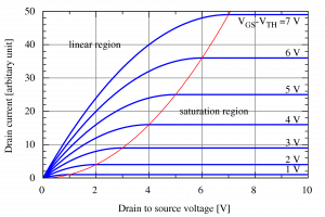
The above graph shows the I-V characteristics for the transistor.
In the particular graph, the current which flows is ‘0’ for gate voltages underneath Vt. The current has increasing when the gate voltage increases accordingly linearly with Vds for small Vds. As Vds approaches the saturation point Vdsat = VGT, current declines and eventually turn out to be independent.
The pMOS transistors behave in a reverse way than the n-MOS transistor so all voltages and currents are negative here.Here the current flows from source to drain and the fluidity of holes in a silicon is usually lower than that of the electrons.
So, a p-MOS transistor produces less current than n-MOS transistor of same size and features. Here µn and µp = mobility of electrons and of holes in n-MOS and p-MOS transistors, respectively. The mobility ratio µn /µp lies between 2–3. The p-MOS transistors have the identical geometry like a nMOS.
For more about MOSFET and others electronics related article click here

Hi, I am Soumali Bhattacharya. I have done Master’s in Electronics.
I am currently invested in the field of Electronics and communication.
My articles are focused on the major areas of core electronics in a very simple yet informative approach.
I am a vivid learner and try to keep myself updated with all the latest technologies in the field of Electronics domains.
Let’s connect through LinkedIn –