- What is JFET ?
- Types of JFET
- Characteristics of JFET
- BJT vs FET
- JFET vs MOSFET
- Applications
- Advantages & Disadvantages
In this article we will learn about the Field Effect Transistor or FET in details and one of its important type namely, Junction Field Effect Transistor (JFET) in detail.
Field Effect Transistor (FET):
In a field-effect transistor, only an electrical field is used to control the flow of current. FETs are unipolar transistors. Field Effect Transistor (FET) have three terminals, which are Source, Drain, and Gate.
Field Effect Transistor Types
There are two main types of field effect transistor,
- Junction Field Effect Transistor (JFET)
- Metal Oxide Semiconductor Field Effect Transistor (MOSFET) or Insulated-gate Field Effect Transistor or IGFET).
Features of Field Effect Transistor
- Unipolar – In Field Effect Transistor, the conduction is happening either by hole or electron.
- High input impedance − the Field Effect Transistor has high input impedance as input current in FET has flown due to the reverse biasing only.
- Output impedance – FET’s Output impedance is very small.
- Voltage-controlled device − Field Effect Transistor is called the voltage-controlled device as its output voltage is controlled by the gate input voltage only.
- Noise is low − The Noise of Field Effect Transistor is lower than in BJTs as in FET, no junctions present in the conduction path.
- Gain – The Gain is characterized as trans-conductance in Field Effect Transistor.
Junction Field Effect Transistor
JFET is one of the simplest type of field effect transistor which have three terminal semiconductors.
Unlike PNP and NPN transistors, the three terminals of a Junction Field Effect Transistor are,
- Source
- Gate
- Drain
Junction Field Effect Transistor (JFET) working
JFET is a voltage-controlled device as it is controlled by use of a reverse bias voltage to the gate terminal. The channel gets drained and the electric current becomes switched off. A Junction Field Effect Transistor is usually said to be on when there is no voltage between the gate and the source pin.
Junction Field Effect Transistor (JFET) is usually two types as it is used n-type or p-type channel as per working. In the n-type, when the voltage source is connected to the gate is -ve with respect to the source, the current decreases. Correspondingly, when a JFET have a p-type channel, if a positive voltage is applied to the gate with respect to the source the current becomes reduced.
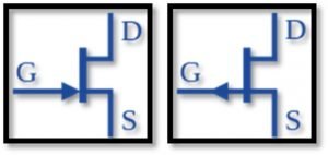
Junction Field Effect Transistor (JFET) Symbol:

Symbol of a JFET


Junction Field Effect Transistor (JFET) Operation:

With VGS=0; applied voltage VDS causes a current to pass through from drain to source terminals.
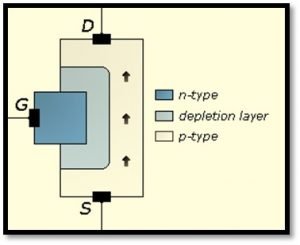
If a negative gate to source voltage is applied, the depletion layer of the gate channel junction widens and channel becomes narrow. Thus, channel resistance is increased and id decreases for a given value of VDS. Because of small value of VDS, the depletion layer is uniform and the device acts as a voltage variable resistance. As value of VGS is increased in negative direction, depletion layer gets widened until it occupies the whole channel. This value of VGS is called the Pinch off voltage (VP).
As VDS appears along the channel length, voltage rises along the channel from source to drain. As a result, depletion layer becomes non-uniform. Reverse bias varies along the channel length and is highest at drain end and the depletion layer is widest at drain end. Hence channel resistance varies along the channel and characteristic curve becomes non-linear.
JFET Parameters:
Transconductance (gm)
In the meantime the, Junction Field Effect Transistor is a voltage controlled current source, the gain is the change in drain current divided by the change in gate voltage. This is termed the transconductance gain (shortened as gm) of the JFET
Transconductance is the ratio of change in drain current (δID) to change in the gate to source voltage (δVGS) at a constant drain to source voltage (VDS = Constant). So gm is fundamentally the slope of change of ID and in respect of change in VGS with constant VDS. It is given by,

This value is maximum at zero the gate to source voltage (VGS = 0). The maximum value (gmo) is specified in particular Junction Field Effect Transistor (JFET) data sheet. . It is usually present in the units of conductance in particularly by unit Siemens. For FET, the standard values of Transconductance (gm) are in range of one to thirty milli siemens.
AC Drain Resistance, ( rd )
It is the resistance between drain and source terminals, when Junction Field Effect Transistor is operating in the Pinch Off region. It is explained as the ratio of (ΔVDS), the variation in drain-source voltage to the variation in drain current (ΔID) at constant VGS – the gate-source voltage. So can be written as

Amplification Factor (µ)
Amplification factor of a Junction Field Effect Transistor specifies just how much more control the gate voltage (VGS) has over the drain voltage (VDS). For example, if µ of a JFET is 30, it signify that VGS is 30 times as effective.

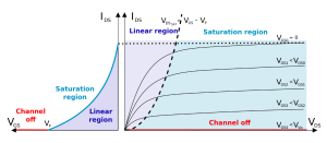
I–V characteristics and output plot of an n-channel JFET

The four different regions of operation for a Junction Field Effect Transistor are explained as follows:
Ohmic Region
If the Gate voltage is zero (VGS = 0) then the depletion layer is very minimal and the Junction Field Effect Transistor perform as a voltage controlled resistor.
Cut-off Region
During the Cut-off region, VGS – the Gate voltage, is sufficient to cause the Junction Field Effect Transistor to act as an open circuit as the channel resistance is at maximum. The Cut-off region is sometimes termed as pinch-off region also.
Saturation or Active Region
During the Saturation region, the Junction Field Effect Transistor acts as a good conductor and is controlled by VGS– the Gate-Source voltage. Whereas during that period the drain to source voltage, (VDS) has little or negligible influence.
Breakdown Region
In the Breakdown Region, The VDS – the voltage between the Drain and the Source, must be sufficiently high to causes the Junction Field Effect Transistors acts as a resistive passage to break down and to permit uncontrolled current.
Advantages of JFET:
- High input impedance
- Low noise
- Small size
- High frequency response
Disadvantages of JFET:
- Junction Field Effect Transistor (JFET) has small gain bandwidth product
- It has more vulnerability to damage during handling and maintenance.
Applications of JFET:
- JFET is used as a switch
- Junction Field Effect Transistor is used as an amplifier.
- It can be used as buffer
- Junction Field Effect Transistor (JFET) is used in digital electronics circuitry because of its size and applicability.

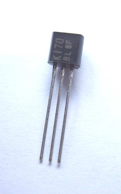
Image Credit:Euler666, Encapsulado JFET, CC BY-SA 3.0
BJT vs FET:
| BJT | FET | |
| Polarity | Bipolar device | Unipolar device |
| Types of Carrier | Electrons and Holes are two types of carrier | Either electrons or holes are required here. |
| Process of Movement | Movement of carrier is made by diffusion process. | Movement of carriers are done by drift. |
| Switching Speed | Switching speed of BJT is comparatively faster. | Switching speed is comparatively slower. |
| Temperature Dependency | Less temperature stable | More temperature stable |
| Noise | Noise level higher | Noise level less |
| Size | Comparatively bigger | Comparatively smaller, used in IC. |
| Price | Comparatively cheaper | Comparatively expensive |
| Control Parameter | Current control device | Voltage Control device. |
| Input Impedance | Low input impedance | High input impedance (in order of 1010 ohms) |
| Gain | Characterized by Voltage gain | Characterized Transconductance |
To know more about electronics click here

Hi, I am Soumali Bhattacharya. I have done Master’s in Electronics.
I am currently invested in the field of Electronics and communication.
My articles are focused on the major areas of core electronics in a very simple yet informative approach.
I am a vivid learner and try to keep myself updated with all the latest technologies in the field of Electronics domains.
Let’s connect through LinkedIn –