A D Flip Flop stores a single bit of data; its output mirrors the input (D) when the clock (CLK) is high. Truth table: When CLK=1, if D=0, output Q=0, if D=1, Q=1; When CLK=0, Q remains unchanged. It’s edge-triggered, changing state only at clock edges, ensuring stable data storage and synchronization in digital circuits. Ideal for shift registers, data storage, and synchronizing asynchronous inputs.
A flip flop is the fundamental sequential circuit element, which has two stable states and can store one bit at a time. It can be designed using a combinational circuit with feedback and a clock. D Flip-Flop is one of that Flip Flop that can store data. It can be used to store data statically or dynamically depends on the design of the circuit. D Flip-Flop is used in many sequential circuits as register, counter, etc.
What is D flip flop ?
D flip-flop or Data flip flop is a type of flip Flop that has only one data input that is ‘D’ and one clock pulse input with two outputs Q and Q bar. This Flip Flop is also called a delay flip flop because when the input data is provided into the d flip-flop, the output follows the input data delay by one clock pulse.
Full Form of D flip flop
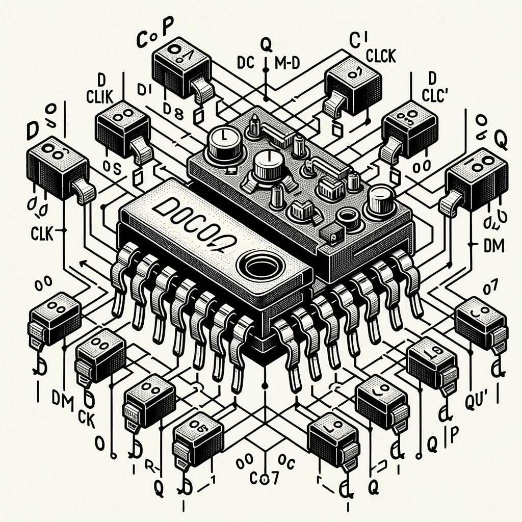
D stands for Delay or Data in D flip-Flop.
D flip flop Diagram
The given circuit represents the D flip-flop circuit diagram, where the whole circuit is designed with the help of the NAND gate. Here the output of one NAND gate is feed as one input to the other NAND gate, which forms a latch. Then, the latch is gated with two more NAND gates where D is one input and clock is the other input.
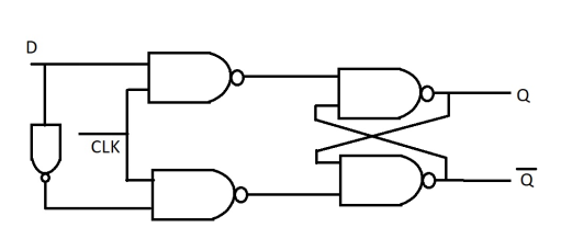
The final output of the D flip-flop is Q and Qbar, where Qbar is always complementary to Q.
D Flip Flop Truth Table
What is D Flip Flop Truth Table ?
The truth table of the d flip flop shows every possible output of the d flip-flop with the all possible combination of the input to the d flip flop, where Clock and D is the input to the D flip-flop and Q and Qbar is the output of the D flip-flop.
| CLOCK | D | Q | Qbar |
| 0 | 0 | NO CHANGE | NO CHANGE |
| 0 | 1 | NO CHANGE | NO CHANGE |
| 1 | 0 | 0 | 1 |
| 1 | 1 | 1 | 0 |
D flip flop Excitation Table
The exaltation table or state table shows the minimum input with respect to the output that can define the circuit. Which mainly represents a sequential circuit with its present and next state of output with the preset input and clock pulse. This table is also known as a characteristic table for D flip-flop.
| Din | CLK | Present state ‘Q’ | Next state ‘Q’ |
| X | 0 | 0 | 0 |
| X | 0 | 1 | 1 |
| 0 | 1 | 0 | 0 |
| 0 | 1 | 1 | 0 |
| 1 | 1 | 0 | 1 |
| 1 | 1 | 1 | 1 |
D flip flop Boolean Expression
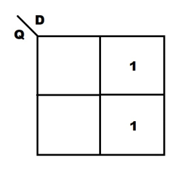
The boolean expression of the D flip-flop is Q(t+1)=D because the next value of Q is only dependent on the value of D, whereas there is a delay of one clock pulse from input D to output Q.
How D Flip Flop Works ?
Working of D flip flop
D Flipflop is a bi-stable memory element, which can store one bit at a time, either ‘1’ or ‘0’. When the D input is provided to the Flip Flop, the circuit check for the clock signal is the signal of the clock is high ( for level triggered d flip-flop) then with every clock pulse, the input D propagates to the output Q.
For edge triggered flip-flop, the circuit check for the transition of clock pulse according to which the flip Flop propagates the input to the output; edge triggered can be positive edge triggered or negative triggered. Positive edge triggered D flip-flop changes its output according to input with every transition of the clock pulse from 0 to 1. As for the negative edge triggered D flip-flop changes its output according to input with every transition of the clock pulse from 1 to 0.
D flip flop Timing Diagram
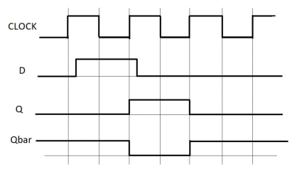
As shown in the given figure, there is a clock pulse representation, with which D, which is the input to D flip-flop, and Q which is the output, is represented, where Qbar is the complement output of the output Q, here we see the timing diagram of a positive edge flip flop, that’s why here the output changes with every positive transition in the clock pulse according to the input.
D flip flop Block Diagram
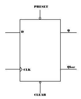
The diagram shown below is the block representation of the d flip-flop, where D is the input, the clock is another input to the Flip Flop, where a preset and clear signal is used to set or reset the output Q of the D flip-flop.
What is D flip flop Symbol ?
D flip flop Clear and Preset
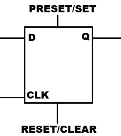
The given figure is the block diagram of a D flip-flop having preset/set and rest / clear as additional input to the Flip Flop, where Preset/Set is used to set the output Q of the flip Flop set to 1. Rest/Clear is to set the output Q of the flip Flop to 0.
D flip flop with Set
D flip-flop can have set the input as a requirement, and it can change the output and set the output Q to 1. It can be synchronous or asynchronous, Synchronous when the output can change only with the clock pulse, asynchronous is when the output can be set to 1 at any point of time regardless of the clock pulse.
D flip flop with Reset
D flip-flop can sometimes reset / clear input only in addition to data input and clock input, resetting the output Q to zero of the d flipflop as a requirement. Reset/Clear be active low input or active high input depends on the Flip Flop design.
Asynchronous Set and Reset
D flip flop with Asynchronous Set and Reset
D flip-flop can have an asynchronous set/preset and reset/clear as input independent of the clock. That means the output of the Flip Flop can be set to 1 with preset or reset to 0 with the reset despite the clock pulse, which means the output can change with or without a clock, which can result in asynchronous output.
D flip flop with Asynchronous Reset
D flip-flops can have asynchronous reset, which can be independent of the clock. Regardless of the clock, the reset can change the output Q to zero, which can cause asynchronous output.
D flip flop with Synchronous Reset
D flip-flop with synchronous reset means the output can reset to zero with the reset input but only with the clock, which makes the reset input dependent on the clock pulse; without clock pulse reset will not be able to set the output Q to zero, which will give you a synchronous output always.
D Flip Flop with Enable
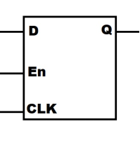
Other than set/preset or reset/clear D flip-flop can have enabled as one input when enable is high, the Flip Flop can operate with the data input and clock input, but when the enable is low then regardless of any other input, the flip Flop stays in a hold state.
D flip flop with Enable Truth Table
| EnableDQn01NO CHANGE00NO CHANGE111100Table: D flip-flop truth table with enable input |
D flip flop Truth Table with Preset and Clear
| PR (ACTIVE LOW) | CLR(ACTIVE LOW) | CLK | D | Q | Qbar |
| 0 | 1 | X | X | 1 | 0 |
| 1 | 0 | X | X | 0 | 1 |
| 0 | 0 | X | X | NOT DEFINED | NOT DEFINED |
| 1 | 1 | 1 | 1 | 1 | 0 |
| 1 | 1 | 1 | 0 | 0 | 1 |
| 1 | 1 | 1 | X | NO CHANGE | NO CHNAGE |
D flip flop Truth Table with Clock and Reset
| CLK | RESET | D | Q |
| 0 | X | X | NO CHANGE |
| 1 | 1 | X | 0 |
| 1 | 0 | 1 | 1 |
| 1 | 0 | 0 | 0 |
Asynchronous D flip flop
When D flip-flop generates output independent of the clock signal, then the output produced may be asynchronous. It is mainly caused by an asynchronous set/preset or clear/reset signal, which can set or reset the output of the flip Flop at any intent of time, which disrupt synchronicity in the D flip-flop.
State Diagram for D Flip Flop
The state diagram is the representation of a different stable state with the transition between the states with the cause of transition. Here every stable state output of the D flip-flop is represented with a circle. In contrast, the transition between the state is represented by the arrow between the circle, which is leveled with the cause of the transition.
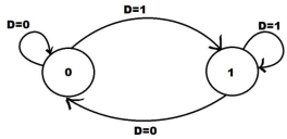
When the state changes from 0 to 1, it is caused by the input D, which is high, and when the output state is 0, and at the time D=0 that produces no change in the output, the arrow with D=0 starts with state 0 and also returns to state 0.
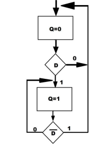
ASM Chart for D flip flop
An algorithmic state machine chart contains three blocks: state block, condition block, and conditional output box. The rectangle box represents one state; the diamond box is the condition box true or false if the condition decides the branch to follow.
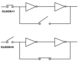
D flip flop schematic | D Flip Flop Schematic Circuit | D Type Flip Flop Schematic
The figure shows the schematic representation of the D flip-flop; the schematic diagram represents the procedure using abstract.
Two diagrams show the working of the D flip-flop when the clock is high and another showing when the clock is low. When the clock is high, the input data passes through the circuit, but when the clock is low, the input can not pass through the circuit, which shows regardless of the change in input, there will be no change in output when the clock is low.
Dynamic D flip flop
Flip Flop is generally a static storing device, but a dynamic flip flop can dynamically store data. In the given schematic diagram of a dynamic flip flop, we can see a capacitor connected to each stage. When there is no clock pulse for a long time, the capacitor’s charge can be lost. However, because of the presence of the capacitor, the circuit will be able to store data dynamically.

Dynamic D flip-flop is designed for faster operation; the area covered by dynamic flip flop is less than that of a static flip flop.
D flip flop Metastability
Metastability refers to the state where output is not deterministic. It can cause oscillation, unclear transitions in the circuitry. For example, flip Flop faces the problem of metastability; it happens to a flip flop when the clock pulse and data change at the same instate of time, which causes the result to behave unpredictably.
To avoid metastability in flip Flop the operation of flip Flop should operate considering the setup time and hold time of the Flip Flop. Still, metastability cannot be eliminated completely, but it can be minimized.
Application of D flip flop
Important applications of D flipflop listed as follows :
- D flip-flop can be used to produce a controlled delay in the circuitry.
- Used to design frequency divider circuity.
- For creating counters.
- For developing registers.
- Used in pipelining.
- For synchronization.
- Can be used to avoid glitches.
- Used to fix clock frequency as for the requirement of the circuitry.
- Can be used for isolation.
- As Toggle switch.
- Can be used for Data transmission.
- Sequence generator.
- Can be used as a memory element.
Difference Between D and T flip flop
| D FLIP-FLOP | T FLIP FLOP |
| The output of a d flip flop follows the input with a delay of one clock pulse. | The output of T flip flop toggles with a high input with every clock pulse. |
| It is known as delay flip flop | It is known as toggle flip flop |
| With low input the output also changes to low with clock pulse | With low input the output does not change at all, it stays in hold state. |
Difference Between D flip flop and JK flip flop
| D flip-flop | J K flip flop |
| The output of a d flip flop follows the input with a delay of one clock pulse. | The output of a J K flip flop sets to 1 with J and resets to 0 with R when there is clock pulse. |
| It is known as delay flip flop. | It is also called universal flip flop. |
| It has less number of input combinations. | It has more number of input combinations. |
Difference Between D latch and D flip flop
| D latch | D flip-flop |
| D latch is a gated SR latch, which do not have clock input | D flip-flop is combination of D latch with clock input |
| Less complex circuit | Complex circuit |
| D latch is has enable signal which can enable or disable the latch operation | D flip-flop has clock signal which can hold or operated the flip flop when no set or reset input is available. |
| D latch can be active high input or active low input latch. | D flip-flop in which data input is always active high, where set or reset input can be active high or active low input. |
| D latch is always a level triggered circuit. | D flip-flop can be level triggered or edge triggered circuit. |
| Less number of transistor is required for design. | More number of transistor is required for design. |
| Asynchronous in nature. | Generally synchronous in nature. |
Q: What is a flip-flop in digital electronics?
A: In digital electronics, a flip-flop or latch is a circuit that has two stable states and can be used to store state information. They are fundamental building blocks in sequential logic, with the D-type flip flop being a commonly-used type.
Q: What is a d-type flip flop?
A: A D-type flip flop is a type of flip flop circuit that has a D (data) input and a clock input. The D flip-flop captures the value of the D-input at a definite portion of the clock cycle (such as the rising edge). This can be thought of as the flip flop “sampling” the D input and storing it.
Q: How do logic gates interact in a d-type flip flop?
A: A D-type flip flop can be implemented using a combination of logic gates such as AND and OR gates, as well as inverters. The particular arrangement of these gates determines the output of the flip-flop for each input condition.
Q: What distinguishes a d-type flip flop from an sr flip-flop?
A: One key difference is that an SR flip-flop requires two inputs, namely S (Set) and R (Reset), while a D-type flip flop takes both a data input and a clock input. Consequently, the behaviour and use cases of these flip flop types are different in digital electronics.
Q: Can you explain the working of a D flip-flop action on the rising edge of the clock?
A: The D flip-flop is sensitive to the clock edge, i.e., the transition from low to high (rising edge) or high to low (falling edge). When the clock signal goes from low to high on the rising edge, the value on the D input is transferred to the flip-flop’s output. At other times, the output remains what was last stored.
Q: How does a D flip flop compare to a JK flip-flop?
A: The JK flip-flop and the D type flip-flop are two types of flip-flops in digital electronics. The JK flip-flop, like the SR flip-flop, has two inputs but does not have the invalid state that the SR flip-flop has when both inputs are 1. The D flip-flop, on the other hand, eliminates this ambiguity by having only one input that determines what state the flip flop will change to, with the change in state being triggered by a clock edge.
Q: How does a D flip-flop function in shift registers?
A: In a shift register, multiple D flip-flops are chained together in a configuration known as a cascade. Each flip-flop passes its output as the input to the next flip-flop on each clock cycle, effectively shifting the binary data held by the register.
Q: What is a truth table in the context of a D flip-flop?
A: A truth table for a D flip-flop is a table that describes how the output of the flip-flop depends on its current output and current input. For a D-type flip-flop, the next state is exactly what the data input is at the time of a positive clock edge.
Q: What is the characteristic equation of a D flip- flop?
A: The characteristic equation of a D flip-flop is simple: The next output Q(next) equals the current input D (Q(next) = D). This is as per data input from the flip flop at the time of a positive clock edge.
Q: How does a delay flip-flop (D FF) work?
A: A delay flip-flop (D FF), sometimes known as a D-type flip-flop, behaves just like a wire delayed by one clock period. It takes an input signal and outputs that same signal, but delayed by one clock cycle. In essence, the D FF “remembers” the input value at the rising edge of the clock and delays it by one clock cycle.
Q: What is an SR flip-flop in digital electronics?
A: An SR flip-flop, one of the types of flip-flops in digital electronics, is a form of a sequential logic circuit often utilized for data storage. An SR flip-flop requires two inputs, specifically, the set (S) and reset (R) inputs. The output changes or retains its state when it faces different input conditions, making it a fundamental building block of digital electronics.
Q: How does a D-type flip flop work?
A: A D-type flip-flop operates with a data input and a clock input. At the rising edge of the clock input, the d-type flip flop transfers the input data to the output. Thus, it acts as a delay or edge-triggered device in digital electronics, transmitting the data input from the flip flop’s input to its output during clock pulses.
Q: What is a JK flip-flop?
A: A JK flip-flop is another type of flip flop circuit found in digital logic. It extends the functionality of the SR flip flop by addressing the input condition issue where both inputs are 1. With a JK flip-flop, this state triggers a toggle, causing the flip flop to change state at every clock edge.
Q: What are logic gates, and how do they relate to flip flops?
A: Logic gates are fundamental building blocks in digital electronics that process binary inputs to produce a binary output based on the type of gate. Flip flops, including D-type and SR flip-flops, are composed of interconnected logic gates. The combination of these logic gates determines how a flip flop behaves in terms of its characteristic equation.
Q: Can flip flops be used as shift registers in digital logic?
A: Yes, flip flops can be utilized to implement shift registers in digital logic. A shift register is a sequential device that utilizes flip-flops to store binary data. In a shift register, data is passed from the output of one flip flop to the inputs of the next flip-flop in a cascade configuration, in synchronization with clock pulses.
Q: What are the input signals in a flip flop?
A: The input signals in a flip flop vary depending on the type of flip flop circuit used. For an SR flip-flop, the two inputs are known as set and reset. For a D-type flip-flop, the two inputs are data and clock. An additional input, known as ‘enable’, may be used in certain types of flip-flops.
Q: What happens when a flip flop receives a rising edge input signal?
A: When a flip flop receives a rising edge input signal, i.e., a transition from a low voltage to a high voltage, a state change typically occurs. In a D-type flip flop, for instance, the state of the data input is captured at the moment of the rising edge of the clock and is transferred to the output.
Q: What role does an inverter play in the operation of a flip flop?
A: An inverter, another basic block of digital electronics, plays a crucial role in the functioning of a flip flop. It is used in a flip flop circuit to invert the output, specifically, a high output becomes low, and vice versa. In the SR flip-flop, for instance, an inverted output from one part of the circuit is often looped back as an input to another part, creating a form of feedback that enables the flip flop to maintain its state.
Q: What is meant by ‘since the output of a flip flop would always change’?
A: When we say ‘since the output of a flip flop would always change’, we’re referring to the inherent characteristic of a flip flop as a bistable device. This means that it has two stable states and can transition between these states based on its input. Thus, depending on the input conditions and type of flip flop circuit, the output of the flip flop can change or retain its prior state, making it a crucial component in digital electronics where data storage and transfer are required.
Q: What leads a flip flop to change state?
A: A flip flop changes state based on its input signal(s). For instance, an SR flip-flop changes state when either the Set or Reset input is activated, and a D-type flip flop changes state based on the data input at the moment of a clock edge, especially a rising edge. The change state feature of flip flops makes them pivotal in designing digital systems for various applications, from basic data storage units to complex microprocessors.
I have graduated in Applied Electronics and Instrumentation Engineering. I’m a curious-minded person. I have an interest and expertise in subjects like Transducer, Industrial Instrumentation, Electronics, etc. I love to learn about scientific researches and inventions, and I believe that my knowledge in this field will contribute to my future endeavors.