CONTENTS
- Introduction to 8085 microprocessor
- The main features of 8085 microprocessor
- BUS architecture of 8085 microprocessor
- What is OPCODE & OPERAND?
- Different Sections of 8085 microprocessor
- 8085 Pin Diagram
- Working of different pins
Introduction to 8085 Microprocessor:
8085 Microprocessor
The 8085 is an 8-bit programmable microprocessor chip which was first designed by INTEL in the year 1977 utilizing NMOS transistors.
The main features of 8085 microprocessor are:
- This has total 40 pin.
- Clock (CLK) speed frequency 3-5 MHz
- The 8085 microprocessor is equipped with sixteen address lines, and eight data lines. So, 8085 is termed an 8 bit microprocessor depending upon its database.
- Requires +5V supply to operate.
BUS Architecture of 8085 Microprocessor:
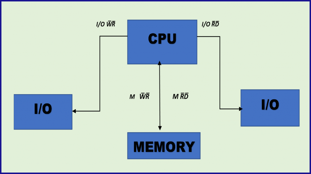
Various I/O devices & memory device are connected to a CPU by group of lines or wires, these are called BUS.
There are three categories of BUS:
ADDRESS BUS
- When the address is sent by CPU, all devices are connected to CPU through address BUS and receives this address but only the device will respond which also receives chip enable signal from CPU. Address BUS is Unidirectional.
DATA BUS
- It carries data values from microprocessor through a memory cell or a peripheral part (memory or I/O write / memory or I/O read). Data BUS is Bidirectional. So, information flows in both way between 8085 microprocessor & memory or I/O device.
CONTROL BUS
- It carries control signal in between Central Processing Unit, memories Input / Output devices. It is also Bidirectional.


I/O M̅ – When the signal is high (logic 1) then CPU wants to communicate with I/O device but when signal goes low (logic o) then CPU will communicate with memory.
R̅D̅ – When CPU sends a low R̅D̅ signal the activated device understands that CPU wants to read information from another device or memory.
W̅R̅T̅ – When CPU sends a low W̅R̅T̅ signal the activated device understands that CPU wants to write information to memory or another device.
What is OPCODE & OPERAND?
OPCODE:
An OPCODE is a signal instruction that can be executed through CPU, without help of opcode any instruction cannot be defined individually.
Example – MOV A, B
Here, MOV means Move, so MOV is OPCODE.
OPERAND:
OPERAND describes an operation such that add, sub, mov on which the operations have to be performed.
Example – MOV A, B
Here, the content of REG B moves to the content of REG A.
Read more about Important Peripherals of 8085 Microprocessor
What are the different sections of 8085 Microprocessor?
There are three categorical area in the 8085 microprocessor;
ALU:
- This section performs the operation of subtraction, addition of logical NOR, compliment, right shifts, left shifts etc.
REGISTER:
- Registers are used for temporary storage of data insertion; it has following register,
- 8 BIT accumulator
- 8 BIT General Purpose Register (B-C, D-E, H-L)
- One 16 BIT Stack Pointer
- One 16 BIT Program Counter
- Instruction Reg, Status Reg, Temporary Reg
TIMING & CONTROL:
- These is primarily responsible for the time & control signal generation which are utmost essential for completing the instruction operation. It can control the data flow between CPU & peripheral device & it provides the timing signal for the operation of memory & I/O devices.
Examples of instructions:
- 1 BYTE Instruction – MOV B, C
- 2 BYTE Instruction – MVI B, 05
- 3 BYTE Instruction – LHLD 5000H
PIN Diagram of 8085 Microprocessor:
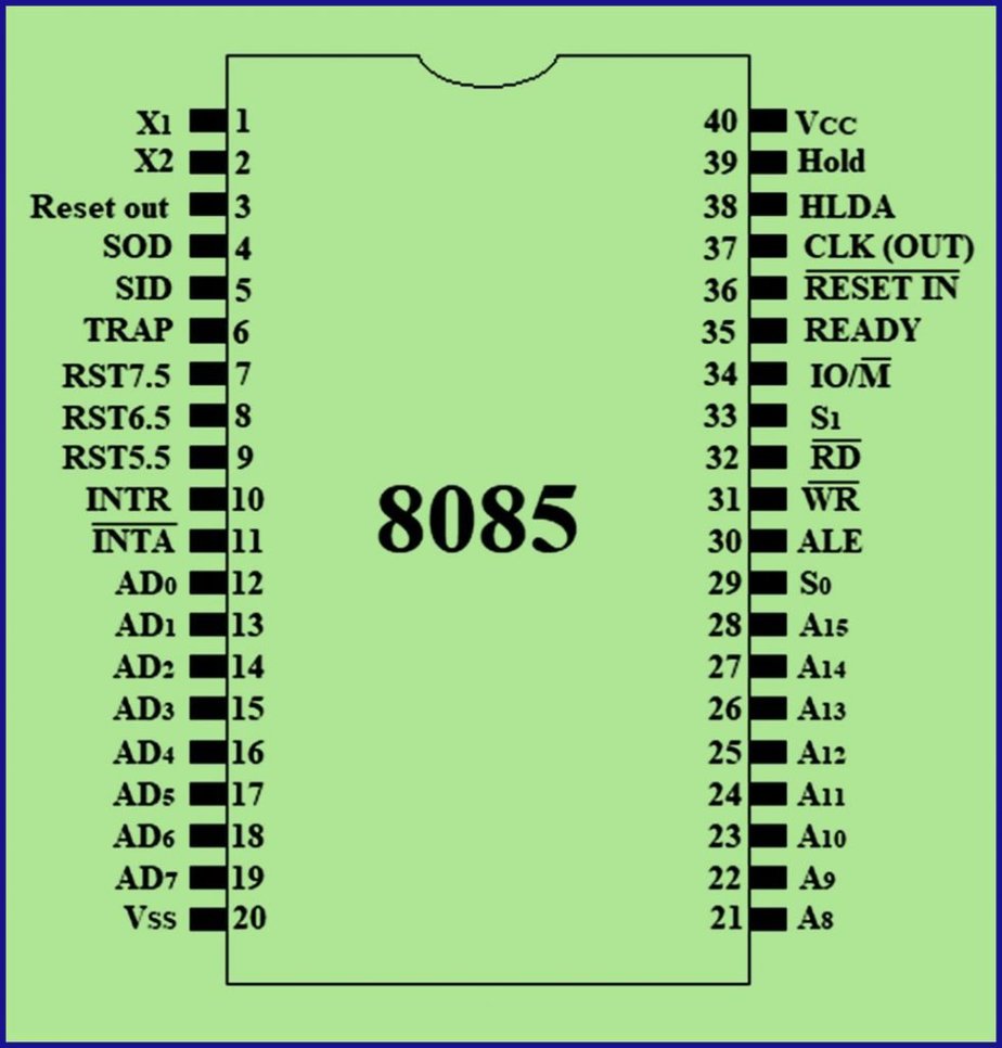
The below image represents description of PINS of a 8085 microprocessor.

| I/O M̅ | S1 | S0 | OPERATION |
| 0 | 0 | 0 | Halt |
| 0 | 0 | 1 | Memory write |
| 0 | 1 | 0 | Memory read |
| 0 | 1 | 1 | Fetch |
| 1 | 0 | 0 | Halt |
| 1 | 0 | 1 | I/O write |
| 1 | 1 | 0 | I/O read |
| 1 | 1 | 1 | Fetch |

Descriptions of the Pins of 8085 Microprocessor:
A8 – A15:
- These address buses are used to be most significant bits of the memory address of 8 bit I/O device.
AD0 – AD7:
- When the address is multiplexed with the data then it is called AD Bus. The lower order or low significant bus as well as the data bus are used for memory address or I/O address.
ALE
- The ALE pin is activated for the first cycle & enable to lower 8 bit of the address data bus to be latched (logic 0) & when ALE is logic 1 then address bus is activated.
| I/O M̅ | S1 | S0 | OPERATION |
| 0 | 0 | 0 | Halt |
| 0 | 0 | 1 | Memory write |
| 0 | 1 | 0 | Memory read |
| 0 | 1 | 1 | Fetch |
| 1 | 0 | 0 | Halt |
| 1 | 0 | 1 | I/O write |
| 1 | 1 | 0 | I/O read |
| 1 | 1 | 1 | Fetch |
I/O M̅:
- It is a status signal for memory as I/O device. When the signal goes high it operates for all I/O devices. When the signal goes low, it works for memory.
R̅D̅:
- It is a signal to control read operation; when the signal is low then it reads the data from I/O device or O/P device.
W̅R̅T̅:
- It is the specified write control signal. This signal specifies the data on the data bus will be written into a designated memory or I/O device.
READY:
- It is active high I/P control signal. It is employed by µP to identify whereas a peripheral has finished the data transfer or not.
HLDA:
- This is the hold acknowledgement signal which is used for granting the hold request.
INTERRUPT:
- TRAP: It has the highest priority over all the interrupts. If any emergency situation comes then it will work.
- RST 7.5: The next priority after TRAP is RST 7.5
- RST 6.5: The next priority after RST 7.5 is RST 6.5
- RST 5.5: The next priority after RST 6.5 is RST 5.5
INTR R:
- It is an interrupt request used as general purpose interrupt. It has the lowest priority.
I̅N̅T̅A̅:
- This signal is interrupt acknowledgement; is used to acknowledge all the interrupts.
RESET IN:
- If the signal on this pin goes LOW, then the device program counter is being set to zero and when it is up it is in reset condition.
RESET OUT:
- This signal designates the up is being reset and be utilized as to reset a memory device and input output devices.
SID:
- Serial I/P data is the data line for signal i/p which is loaded into the accumulator’s 7th bit location.
SOD:
- Serial o/p data is the 7th bit of the accumulator is o/p on the SOD line.
X1 – X2 [clock input]:
- These are two input perform as a clock input.
CLOCK O/P:
- The frequency is the same in which process operate.
VCC & GND:
- VCC is connected to +5V; and GND pin is Grounded.
For more Electronics related article click here

Hi, I am Soumali Bhattacharya. I have done Master’s in Electronics.
I am currently invested in the field of Electronics and communication.
My articles are focused on the major areas of core electronics in a very simple yet informative approach.
I am a vivid learner and try to keep myself updated with all the latest technologies in the field of Electronics domains.
Let’s connect through LinkedIn –