CONTENTS
- What is a tunnel diode
- Tunnelling
- V-I characteristics
- Circuit diagram
- Symbol
- Applications
- What is Schottky diode
- V-I characteristics
- Circuit diagram & symbol
- Applications
What is a Tunnel Diode?
Definition of a Tunnel Diode:
“A tunnel diode is a type of semiconductor diode that has effectively negative resistance due to the quantum mechanical consequence known as ‘tunnelling effect.”
The depletion layer constitutes by a potential barrier at the junction. The potential barrier usually obstructs the flow of carriers from one to other side of the junction. If the concentration of impurity is significantly increased the device characteristics gets completely changed. A new diode by Esaki, gave the correct theoretical explanation for diode’s volt-ampere characteristic.
What is tunneling effect in semiconductors?
The Tunneling Effect or Tunneling Phenomenon:
“Tunneling is a purely quantum-mechanical procedure by which a microscopic particle can infiltrate a potential barrier even when the energy of the incident particle is lesser than the potential barrier.”
The width-size of the junction barrier inversely proportional to the square root of impurity concentration. This quantum mechanical behaviour is termed as ‘tunnelling’, and these p-n junction devices with high impurity concentration are called tunnel diodes.
Symbol of a Tunnel Diode:
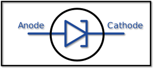
Characteristic of Tunnel Diode:
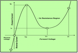
A tunnel diode is a great conductor in the opposite direction. Also the resistance is less for little forward voltage. In the current IP known as peak current is corresponding to the voltage VP, the change in current to voltage (dI/dV) ratio stays 0. The tunnel diode displays a negative resistance characteristic involving the peak current IP and minimal value IV known as the valley current.
In the valley voltage VV, where I=IV, the conductance is ‘0’ and further than this point, the resistance gets positive. For the peak forward voltage VP, the current again touches the IP for more applied voltages the current can increases more.
For this characteristics, the tunnel diode can be utilized in multiple device such as pulse and digital applications.
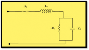
The negative resistance -RD has a minimum between IV and IP point. The series resistance is commonly termed as ohmic resistance (RS). The series inductance (LS) be influenced by the terminal length and the geometry. The junction capacitance CD depends upon the bias and usually is measured at the valley point. Switching times of the order of a nanosecond are in practical application, and switching times as low as 50 pico-seconds have been achieved.
Materials of a Tunnel Diode:
The Most Economical Commercially accessible tunnel diodes are created from Germanium and Gallium Arsenide semiconductors. It’s Hard to produce a metal tunnel diode using a high ratio of IP/IV or by the peak-to-valley current.
Typical Tunnel diode parameters
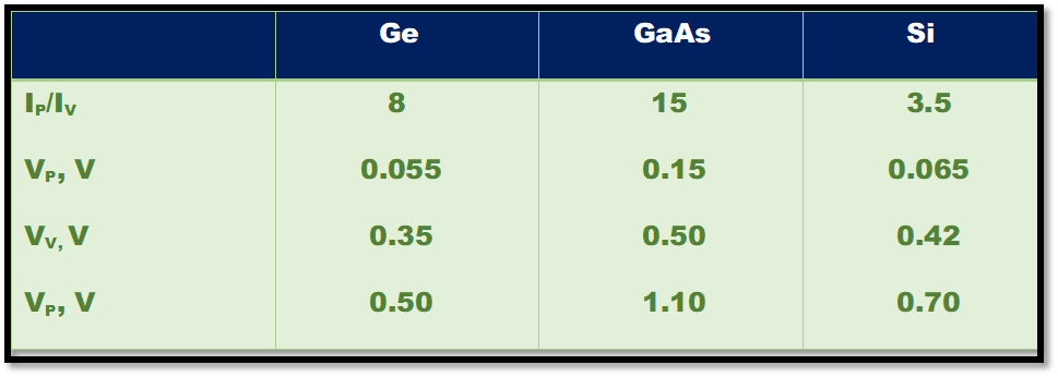
From the above table, we can summarize the important static characteristics of these devices. The voltage values in the table are determined principally by the particular semiconductor used and are almost independent of the current rating. The peak current (IP) is measured by the impurity concentration and the area of junction.
What are the advantages & disadvantages of Tunnel Diode?
Advantages of tunnel diodes are
- low noise
- Simplicity.
- higher speed of operation
- Resistance to extreme environments.
- Less power requirement.
- Comparatively less expensive.
Disadvantages of Tunnel diode are
- Tunnel Diodes are two-terminal devices, so no isolation between output and input. Sometimes, it could lead to serious circuit-design difficulties.
- Low output-voltage swing obtained.
What is Schottky Barrier Diode?
Among the earliest practical semiconductor apparatus used in the early 1900s was that the metal-semiconductor diode. The diode, also referred to as a point contact diode, was created by attaching a metallic part into a bare semiconductor surface. These metallic semiconductor diodes weren’t readily duplicated or automatically reliable and were substituted by the p-n intersection. But, semiconductor and vacuum technologies is currently utilized to manufacture reproducible and reliable metal.
Symbol of Schottky Diode:
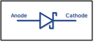
Qualitative Properties of Schottky Barrier Diode:
The Metal and semiconductor band diagrams when separated (top) and when in contact (bottom).
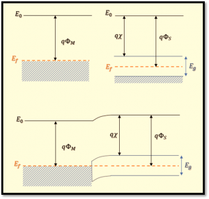
The perfect energy band diagram for a specific metal and n-type semiconductor prior to constructing contact is revealed. The vacuum level is used as a benchmark level. The parameter Øm is that the metal work function, ØS is your semiconductor work function and X is popularly referred to as the electron affinity. As a way for fermi level to develop into a continuous throughout the system in thermal stability, electrons in the semiconductor flow in the lower energy states from the alloy. Positively charged donor atoms stay in the semiconductor developing a space charge region.
Voltage-Current (V-I) characteristic of Schottky Diode:
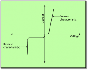
The general shape of the metal semiconductor Schottky diode I-V characteristics are similar to a standard p-n junction diode.
P-N junction diode VS Schottky Diode:
| Parameter | PN JUNCTION DIODE | SCHOTTKY DIODE | ||
| Polarity | It is a Bipolar device | It is a Unipolar device | ||
| Junction | It had Semiconductor to semiconductor junction. | It has Semiconductor to metal junction formation | ||
| Voltage drop | Large forward voltage drop | Lower forward voltage drop | ||
| State loss | On state losses will be more | Low on state losses | ||
| Suitability | Suitable for low frequency applications | Suitable for high frequency switching applications | ||
Applications of Schottky Diode:
- The Schottky Diode utilized as rectifiers in switched mode power supplies (SMPS)
- Schottky Diodes are in different solar cell applications.
- They are used in different logic gate implementations
- Schottky Diode can be used for AC to DC converter circuit.
- In different detector applications they are also employed.
To know more about diodes click here

Hi, I am Soumali Bhattacharya. I have done Master’s in Electronics.
I am currently invested in the field of Electronics and communication.
My articles are focused on the major areas of core electronics in a very simple yet informative approach.
I am a vivid learner and try to keep myself updated with all the latest technologies in the field of Electronics domains.
Let’s connect through LinkedIn –