What is an NPN Transistor ?
BJT or Bipolar Junction Transistor has two main types. N-P-Nis one of the classifications of BJT. It is a three terminal device and used for amplification and switching.
This transistor also consists three sections, they are
- B-Base
- C- Collector
- E- Emitter
- The NPN emitter is used to supply charge carriers to the collector through the base.
- The Collector area gathers charge carriers from the emitter region.
- The base of the transistor does the job of triggering and it works as the controller to limit the amount of current that will be allowed to go across this region.
Note:
Unlike a MOSFET where only one carrier is present, the BJT has two types of charge carrier – Majority and Minority. In case of NPN transistor, the electrons are the majority charge carrier.
Conversely, in P-type semiconductors, electrons aren’t available much, and the hole acts as a majority charge carrier and current will be carried through because of them.
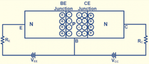
n-p-n transistor construction:
The diagrammatic representations of n-p-n transistors are given below.


The NPN transistor’s equivalent circuit.
We can say that the working of a n-p-n transistor is similar to the working of 2 p-n junction diode connected one after another. These PN junction diodes are termed as the collector-base C-B junction and base-emitter B-E junction.
Consideration as per Doping:
- The emitter section is heavily doping section. The general rule is to keep the base’s width minimum among all the three terminals. As emitter is heavily doped, it can shoot up charge carriers to the base regions.
- As mentioned earlier, the base has the minimum width and it also has the minimum doping. The base passes numerous charge carriers to the collector, which is carried from the emitter.
- The collector regions is in comparison moderately doped and used for collecting charges from the base region.
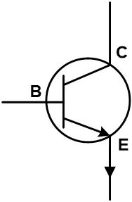
NPN Transistor Symbol

NPN Transistor Pinout
As mentioned earlier, a transistor has three terminals. They are – Base, collector, and emitter.
How to identify NPN Pin?
- In the majority of the configurations, the center part is for the base terminal.
- The pin that is below this is a collector, and also, the rest of one is the emitter pin.
- When the dot isn’t marked, all terminals has to be identified using there orientation or uneven terminal space between pin. Here the center pin is the base. The nearest pin is the emitter, and the rest pin is a collector terminal.
Applications of NPN transistors:
- Usually, the NPN transistor is used as bipolar transistor because of electrons’ mobility, as it is higher than the mobility of holes.
- These are also used in amplifying and switching the signals. These are used in amplifier circuits i.e., push-pull amplifier circuits.
- The NPN transistor is used Darlington pair circuits to amplify weak signals to significantly scaling up signal.
- If there is a need to sink current, then also NPN transistors could be used.
- Other than these, NPN transistor has many applications in temperature sensors, circuits like logarithmic converters, etc.
How Does an NPN Transistor Work?
NPN transistor needs both the reverse and forward bias for working. The forward bias is established between the Emitter voltage and the emitter. The reverse bias is connected between the collector voltage and the collector.

Now, as the n side of a diode has electrons as majority and p side has holes as majority, all the voltage connections get arranged as forward and reverse bias accordingly. The base emitter junction is set as the reverse bias and the collector base junction works as forward bias. The depletion region of this emitter-base area is narrower compared to the depletion area of the collector-base intersection.
As the junction is reverse biased (emitter), the holes flow from the supply to the N junction. Then the electron moves towards the p side. Here, neutralization of some electron occurs. The rest of the electrons move towards the n-side. The voltage drop in respect to the emitter and base is VBE as input side.
In N-type emitters, the charge carrier is mostly electrons. Hence, electrons carried through N-type emitters to a P-type base. A current will be carried through the emitter-base or E-B junction. This current is known as the emitter current (Ie). Here the emitter current (IE) flows from output side and it flows in two directions; one is IB and other is IC. So we can write,
IE=IB+IC
However, the base area is relatively thin and lightly doped. Hence, mostly electrons will pass the base area, and only few will recombine with available holes. The base current is minimum in comparison with emitter current. Usually, it’s up to 5% of the entire emitter current.
The current flowing from the rest of the electrons is referred to as the collector current (IC). The IC is comparatively high when compared with the base (IB).
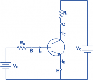
N-P-N Transistor Circuit
The voltage source is connected to the NPN transistor. The collector terminal is joined to the +ve terminal of supply voltage (VCC) using a load resistance (RL). The load resistance can also be utilized to decrease the most current flowing through the circuit.
The base terminal is joined to the +ve terminal of the base provide voltage (VB) with resistance RB. The base resistance is used to restrict the maximum base current (IB).
When the transistor is ON operation, large collector current passing through the circuit between the collector and from the emitter. However, for that little quantity of base current must flowing to the bottom terminal of the transistor.

The markings represents the typical currents of Collector, bas and emitter.
Advantages and Disadvantages of using a NPN Transistor:
Advantages:
- Small in size.
- Can work in low voltage.
- Very cheap.
- Low output impedance.
- Long lasting.
- Spontaneous actions.
Disadvantages:
- High Temperature sensitivity.
- Produce low energy and power.
- Can get damaged during a thermal runaway.
- Cannot be operated in high frequencies.
NPN Transistor Switch
The transistor operates
- Switched ON in the saturation mode
- Switched OFF in the cut-off mode.
Switched ON in the saturation mode
- When both junctions are in the forward bias condition, sufficiently high voltage is applied to input voltage. Hence, the transistor functions as a short circuit as VCE is approximately zero.
- At that time two junctions are in the forward bias state, adequate voltage is in the input.
- In this state, the current will pass between collector and emitter. The current is flowing within circuit.
Switched OFF in the cut-off mode.
- If the two junctions of the transistors are in reverse bias, the transistor goes into OFF state.
- During this mode of operation, the input signal voltage or the base voltage is zero.
- Consequently, the total VCC voltage acts across the collector.
Operating Mode of Transistor
It has three modes of operation as per biasing, are as follows:
- Active mode
- Cut-off mode
- Saturation mode
Cut-off Mode
- The transistor acts as an open circuit.
- In cut-off, the two junctions are in reverse bias.
- The current won’t be allowed to flow through.
Saturation Mode
- The transistor perform as a close circuitry.
- Both junctions are configured in forward bias only.
- As the base-emitter voltage is comparatively high a current pass from collector to emitter.
Active Mode
- In this time, the transistor functions as a current amplifier circuit.
- In the transistor’s active mode, the B-E junction is at forward bias, and the C -B junction is at reverse biased.
- The current passes in between emitter and collector and the quantity of current are proportional to the applied base present.
To know more about electronics click here

Hi, I am Soumali Bhattacharya. I have done Master’s in Electronics.
I am currently invested in the field of Electronics and communication.
My articles are focused on the major areas of core electronics in a very simple yet informative approach.
I am a vivid learner and try to keep myself updated with all the latest technologies in the field of Electronics domains.
Let’s connect through LinkedIn –